Raman Spectroscopy Imaging of Exceptional Electronic Properties in Epitaxial Graphene Grown on SiC

 ,
,  and
and 
Abstract

1. Introduction
2. Silicon Carbide Substrate Properties Directed to Epitaxial Graphene Growth
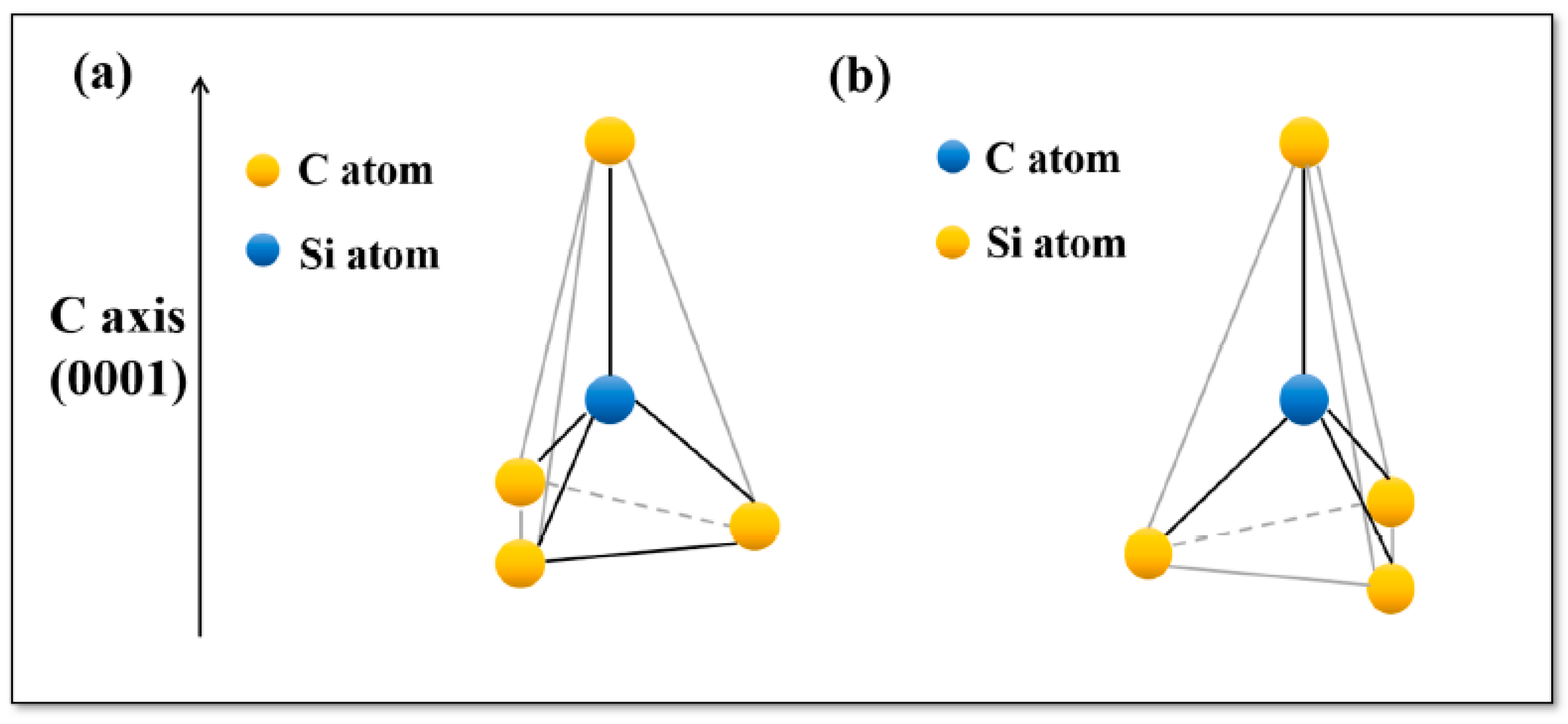
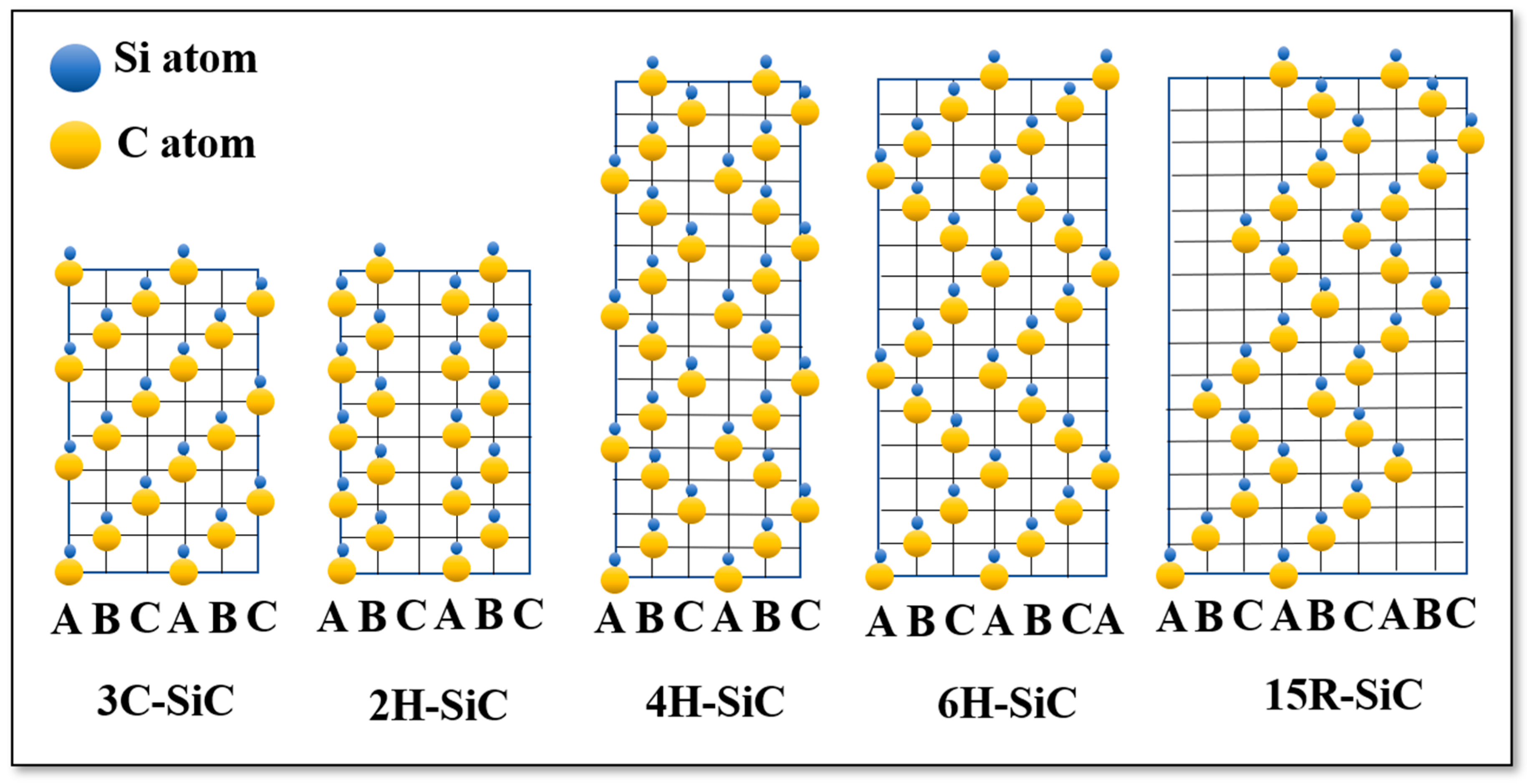
2.1. Structural Properties of Silicon Carbide Polytypes
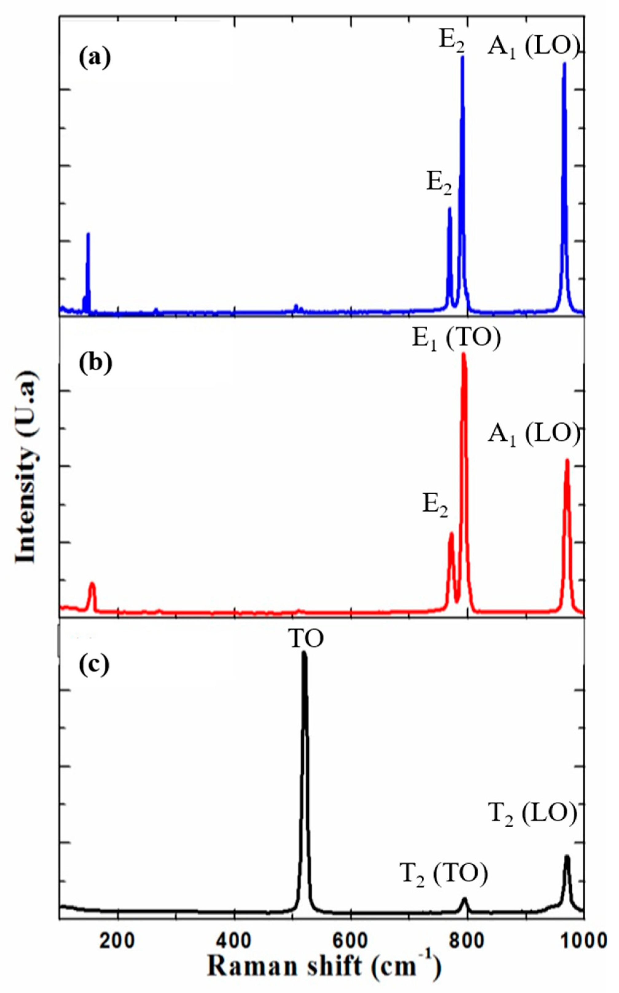
2.2. Raman Signature of SiC Substrate
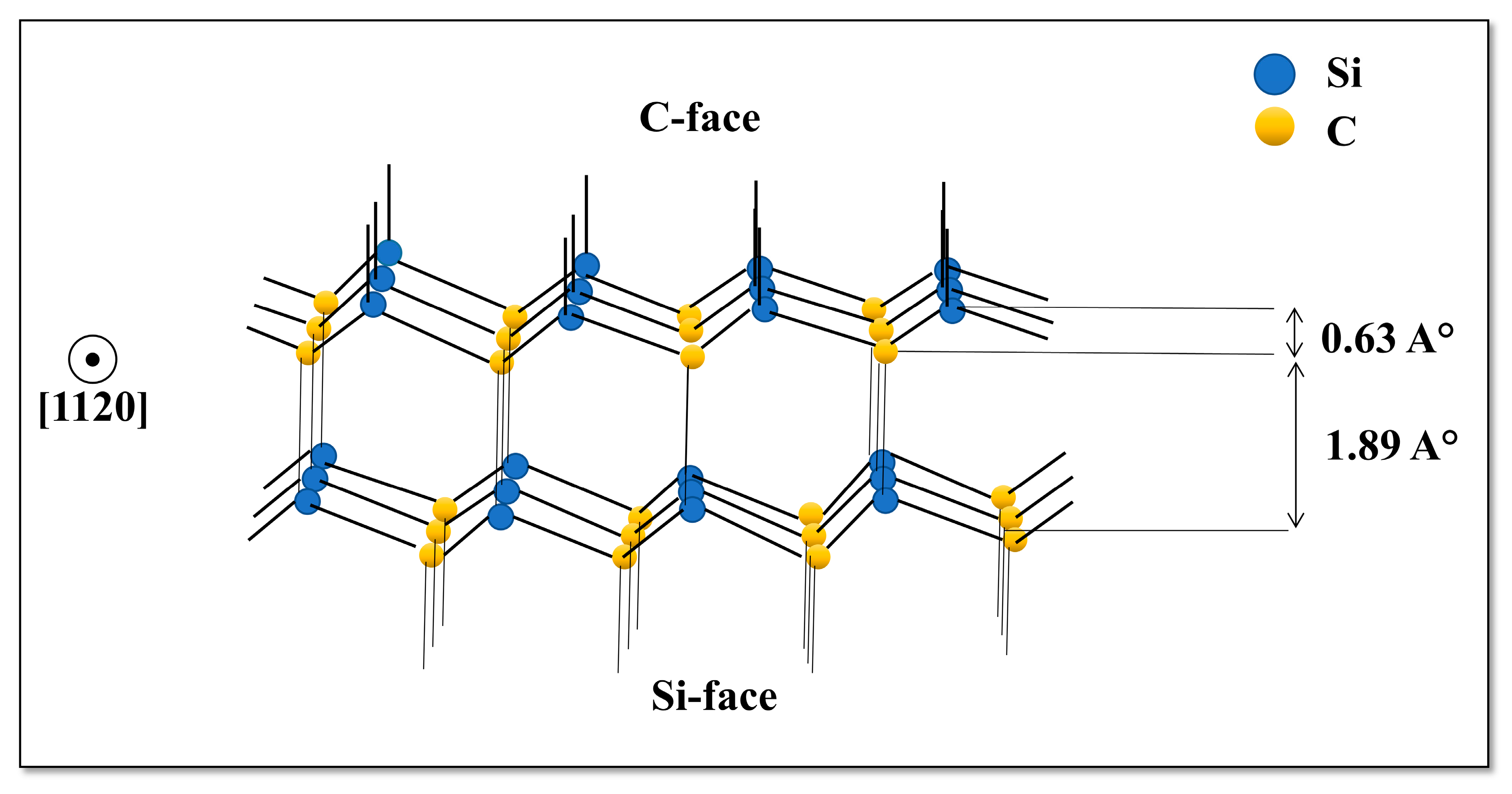
2.3. Polar Behaviour in SiC Substrate
3. Epitaxial Graphene Growth Dependence on the Substrate Polarities
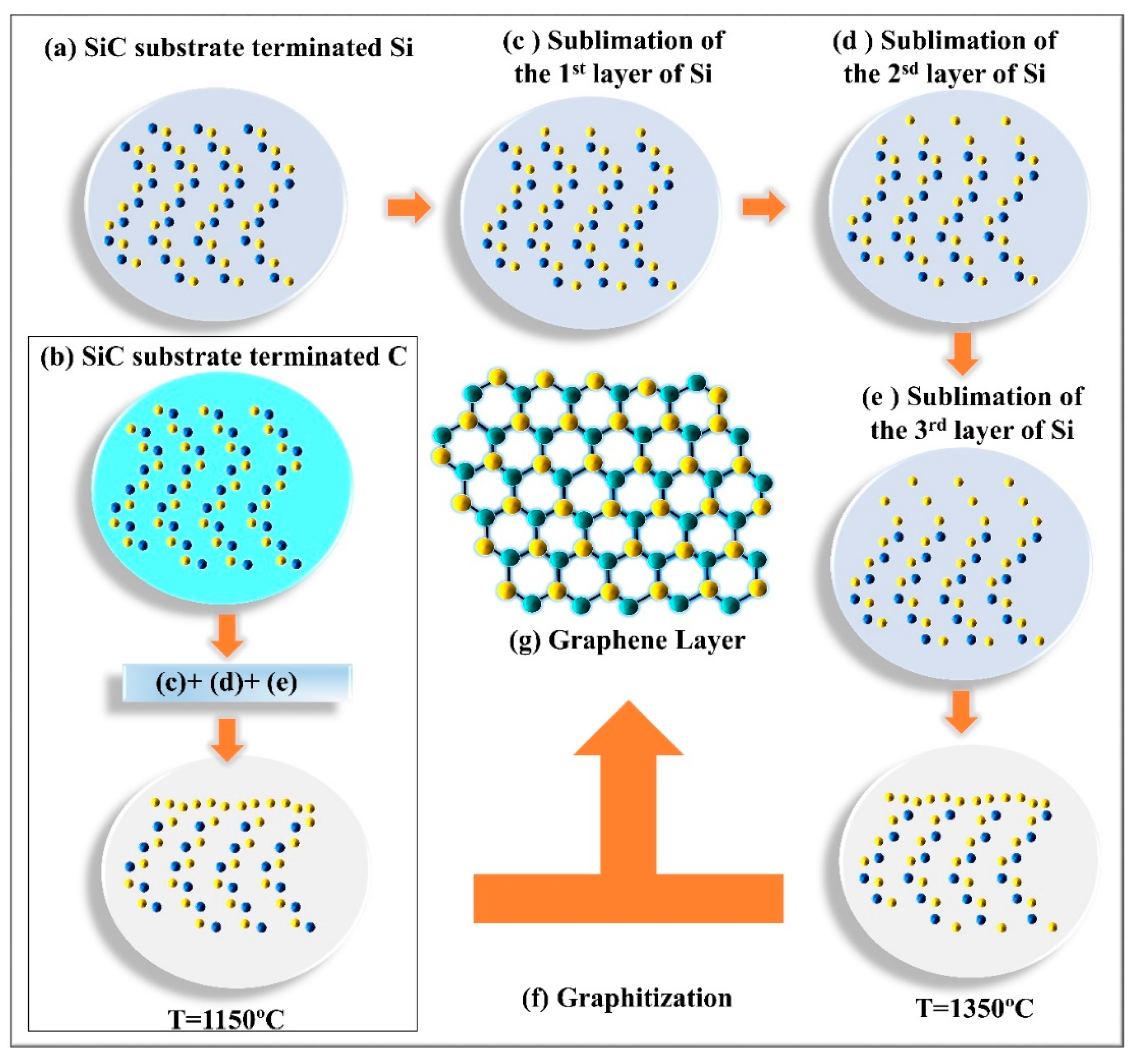
3.1. Si-Face Grown Epitaxial Graphene
3.2. C-Face Grown Epitaxial Graphene
3.3. SiC polarity Effect on the Grown Graphene Layers
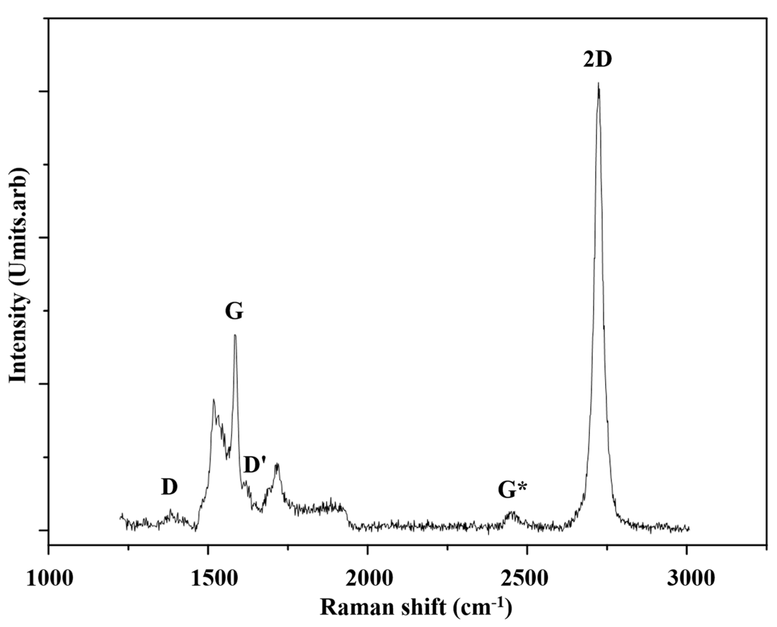
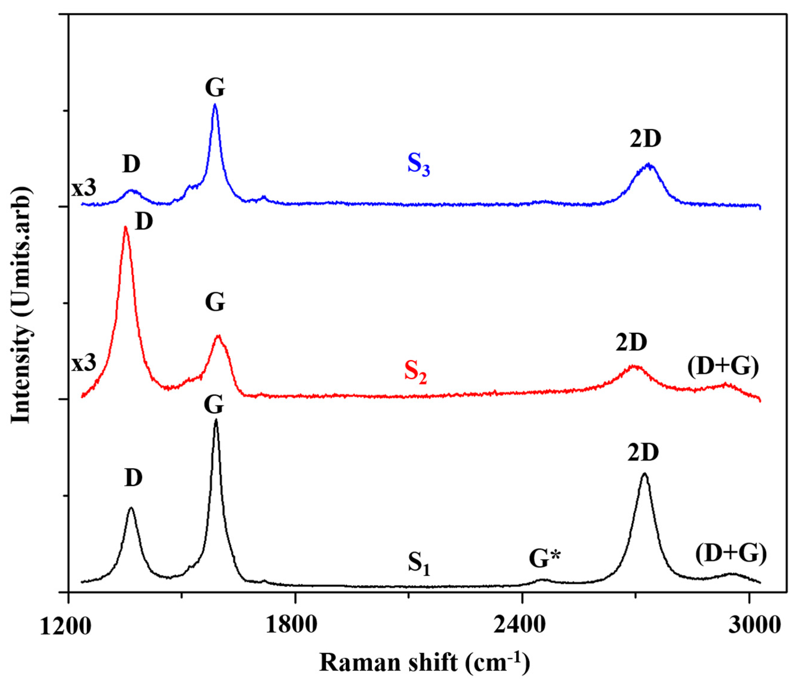
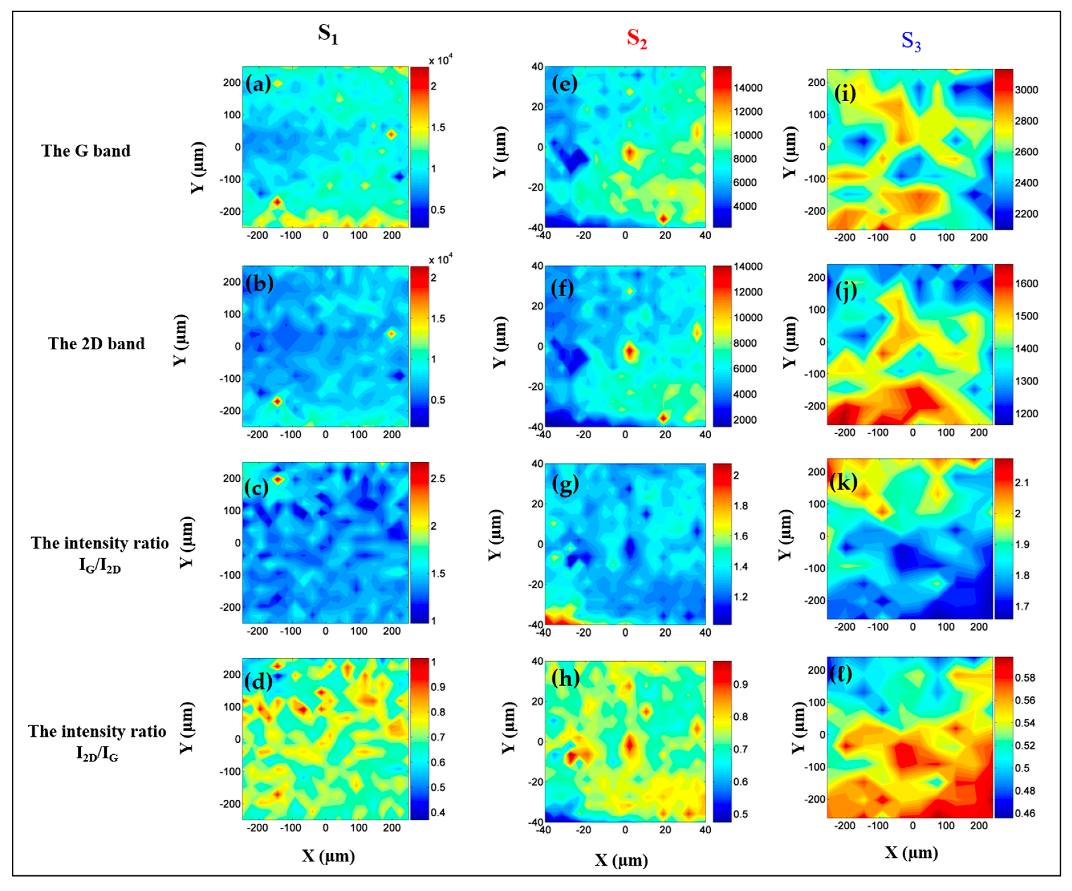
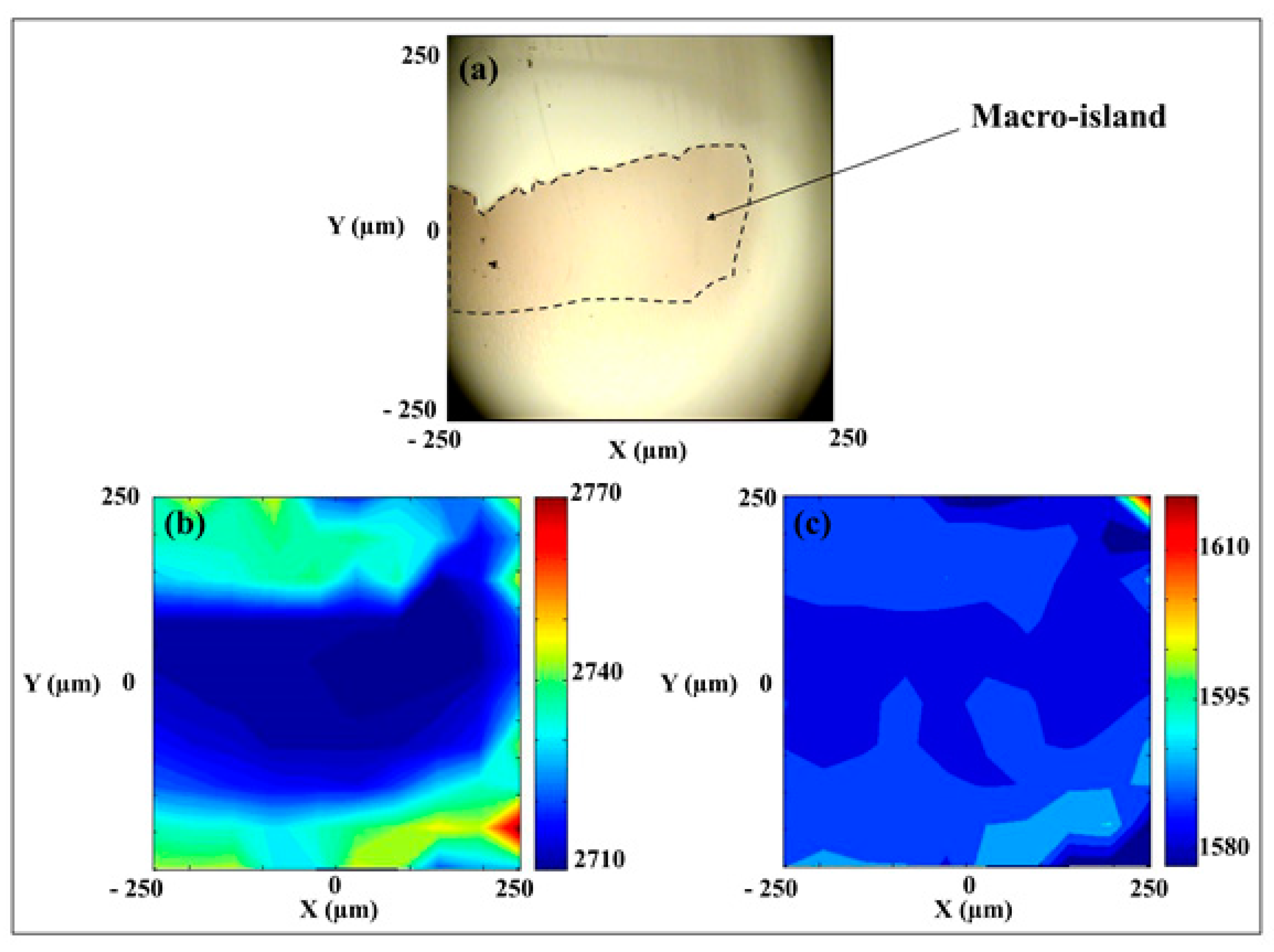
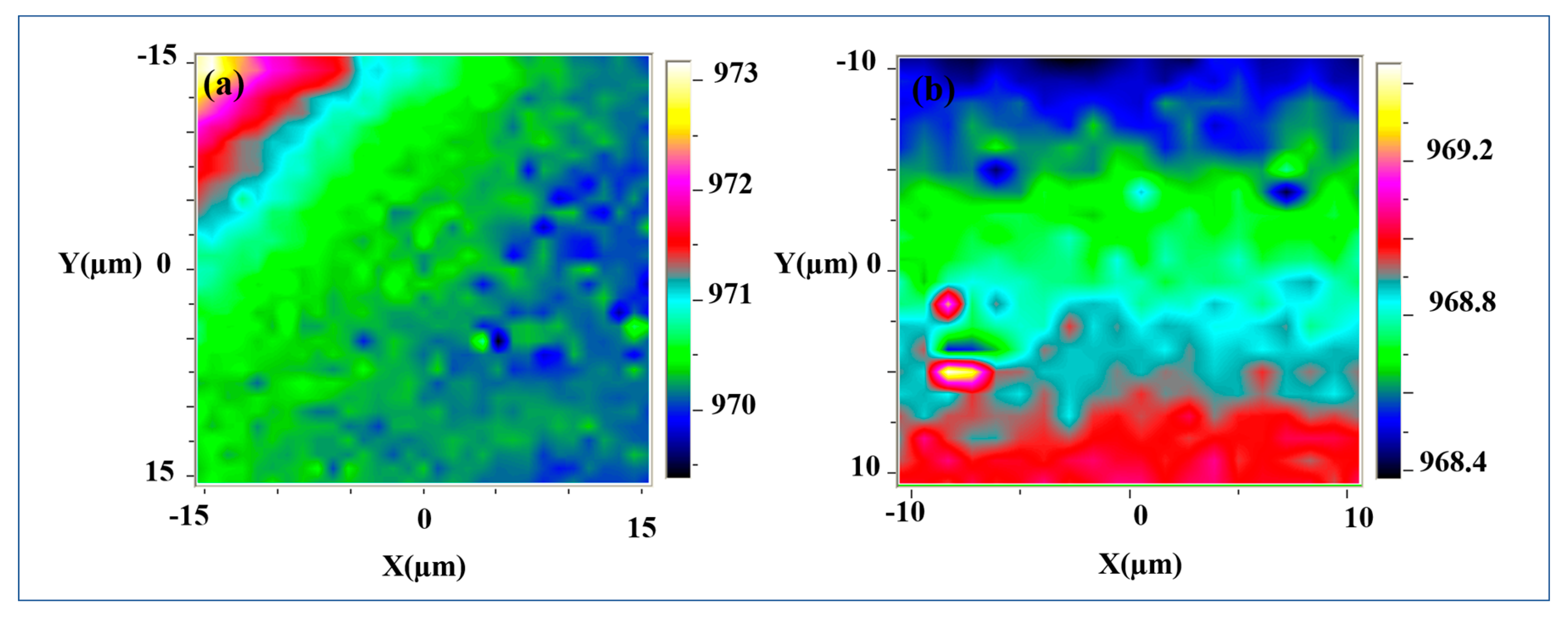
3.4. Raman Signature of Graphene Layer
4. Raman Investigation of Electrical Properties in Epitaxial Graphene
4.1. Raman Spectroscopy and Coherence to Electrical Measurements of Graphene
4.2. Graphene Raman Modes Locating Electrical Properties Changes
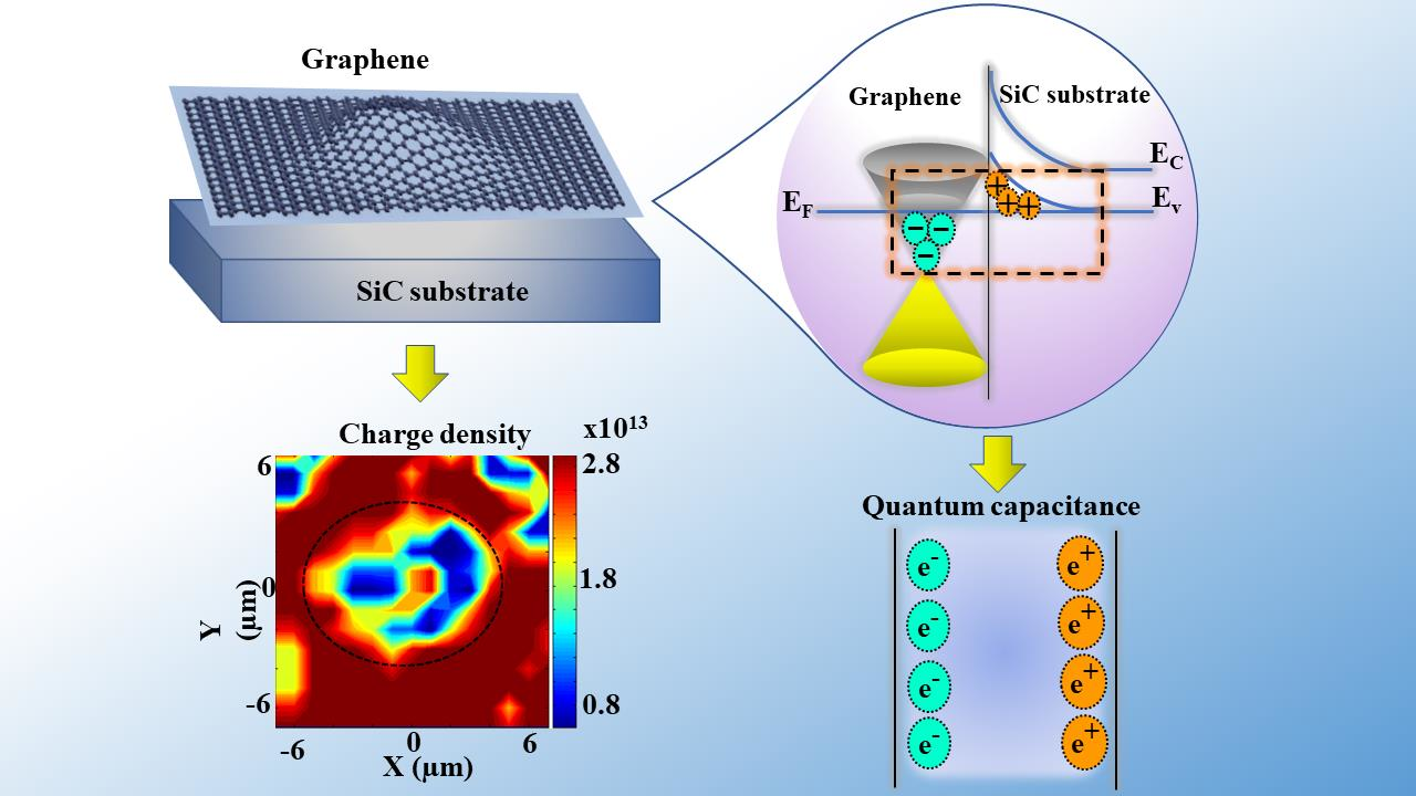
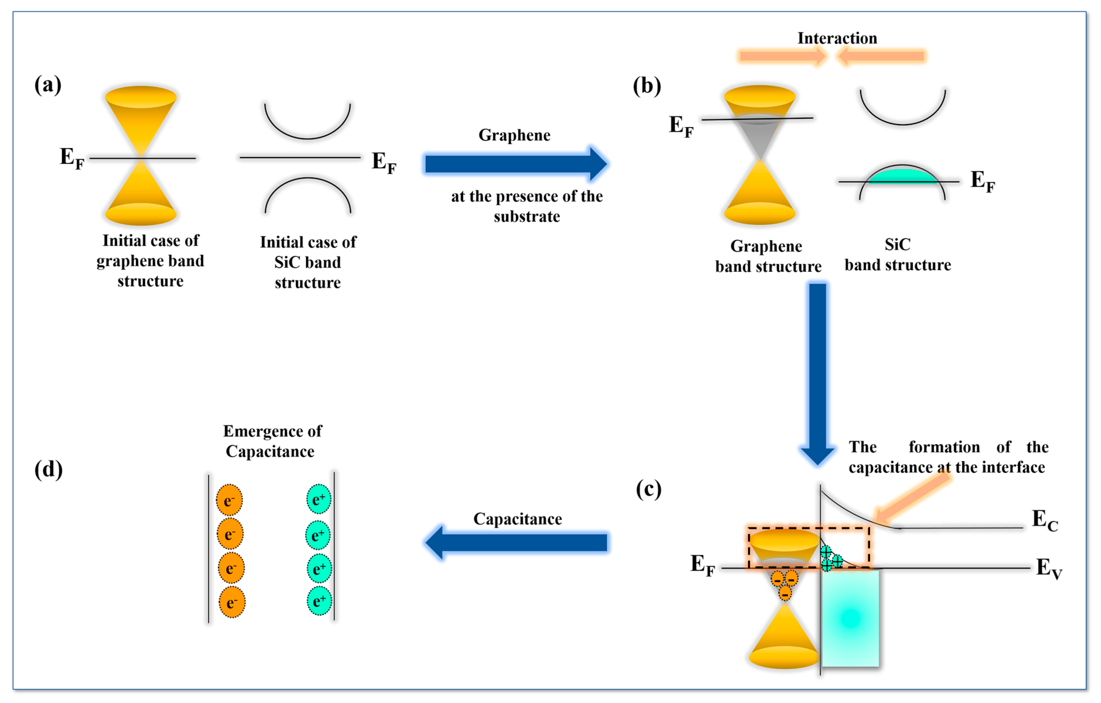
4.2.1. Electrical Properties of Single Layer Graphene: Capacitor Effect and Gap Opening
4.2.2. Electrical Properties of Single Layer Graphene: Substrate Investigation
5. Future Challenges for Raman Spectroscopy to Study Effects of the Lattice Strain or Pseudo-Magnetic Field on Relativistic Dirac Fermions
5.1. Quantum Hall Effect (QHE) and Raman Spectroscopy
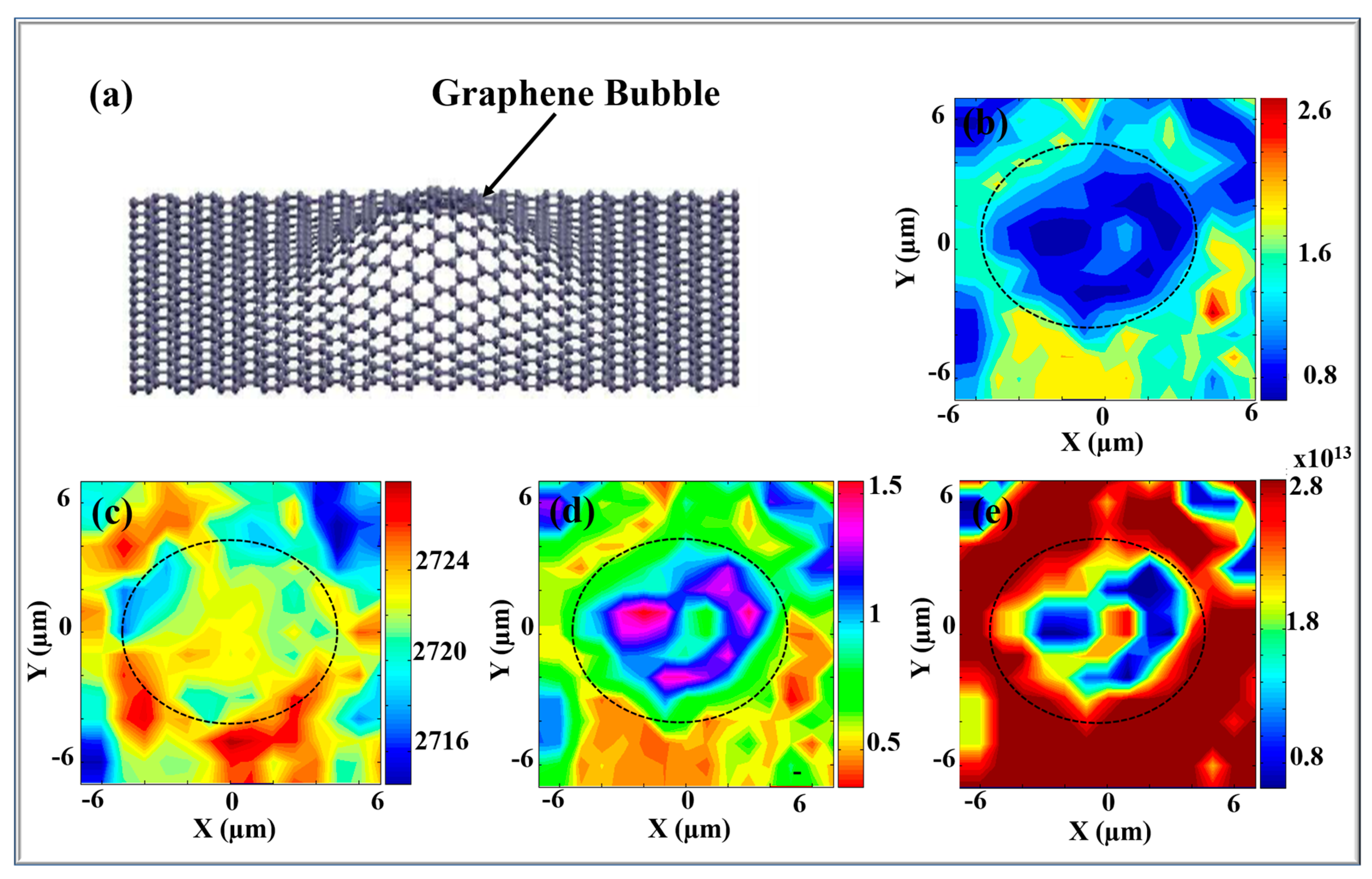
5.2. Graphene Flatness, Nano Domes and Associated Lattice Strain- Geometry Dependent Pseudomagnetic Field and Quantum Spin Hall Effect (QSHE)
5.3. SiC Termination Impact on Landau Quantisation Localised by Raman
5.4. Landau-Phonons Level Crossings
5.5. Homogeneous Strain Originated by Kirigami Art, Perforated Graphene and Epitaxial Graphene-SiC Intercalation: Future Raman Challenges
6. Conclusions
Author Contributions
Funding
Acknowledgments
Conflicts of Interest
References
- Wallace, P.R. The Band Theory of Graphite. Phys. Rev. 1947, 71, 622. [Google Scholar] [CrossRef]
- Novoselov, K.S.; Geim, A.K.; Morozov, S.V.; Jiang, D.; Zhang, Y.; Dubonos, S.V.; Grigorieva, I.V.; Firsov, A.A. Electric Field Effect in Atomically Thin Carbon Films. Science 2004, 306, 666–669. [Google Scholar] [CrossRef] [PubMed]
- Novoselov, K.S.; Geim, A.K.; Morozov, S.V.; Jiang, D.; Katsnelson, M.I.; Grigorieva, I.V.; Dubonos, S.V.; Firsov, A.A. Two-dimensional gas of massless Dirac fermions in graphene. Nature 2005, 438, 197–200. [Google Scholar] [CrossRef] [PubMed]
- Seung, H.S.; Nelson, D.R. Defects in flexible membranes with crystalline order. Phys. Rev. A 1988, 38, 1005. [Google Scholar] [CrossRef]
- Witten, T.A. Stress focusing in elastic sheets. Rev. Mod. Phys. 2007, 79, 643. [Google Scholar] [CrossRef]
- Peierls, R.E. Bemerkungen uber umwandlungstemperaturen. Helv. Phys. Acta 1934, 7, 81–83. [Google Scholar]
- Berger, C.; Song, Z.; Li, T.; Li, X.; Ogbazghi, A.Y.; Feng, R.; Dai, Z.; Marchenkov, A.N.; Conrad, E.H.; First, P.N.; et al. Ultrathin Epitaxial Graphite: 2D Electron Gas Properties and a Route toward Graphene-based Nanoelectronics. J. Phys. Chem. B 2004, 108, 19912–19916. [Google Scholar] [CrossRef]
- Berger, C.; Song, Z.; Li, X.; Wu, X.; Brown, N.; Naud, C.; Mayou, D.; Hass, J.; Marchenkov, A.N.; Conrad, E.H.; et al. Electronic Confinement and Coherence in Patterned Epitaxial Graphene. Science 2006, 312, 1191–1196. [Google Scholar] [CrossRef]
- Badami, D. X-Ray studies of graphite formed by decomposing silicon carbide. Carbon 1965, 3, 53–57. [Google Scholar] [CrossRef]
- Yazdi, G.R.; Iakimov, T.; Yakimova, R. Epitaxial Graphene on SiC: A Review of Growth and Characterization. Crystals 2016, 6, 53. [Google Scholar] [CrossRef]
- Tang, Q.; Maji, S.; Jiang, B.; Sun, J.; Zhao, W.; Hill, J.P.; Ariga, K.; Fuchs, H.; Ji, Q.; Shrestha, L.K. Manipulating the Structural Transformation of Fullerene Microtubes to Fullerene Microhorns Having Microscopic Recognition Properties. ACS Nano 2019, 13, 14005–14012. [Google Scholar] [CrossRef] [PubMed]
- Dimitrakakis, G.K.; Tylianakis, E.; Froudakis, G.E. Pillared Graphene: A New 3-D Network Nanostructure for Enhanced Hydrogen Storage. Nano Lett. 2008, 8, 3166–3170. [Google Scholar] [CrossRef] [PubMed]
- Sheka, E.F.; Chernozatonskii, L.A. Uncertainty and bias in contrast concentration measurements using spoiled gradient echo pulse sequences. J. Comput. Theor. Nanosci. 2010, 7, 1814–1824. [Google Scholar] [CrossRef][Green Version]
- Wilson, P.M.; Mbah, G.N.; Smith, T.G.; Schmidt, D.; Lai, R.Y.; Hofmann, T.; Sinitskii, A. Three-dimensional periodic graphene nanostructures. J. Mater. Chem. C 2014, 2, 1879–1886. [Google Scholar] [CrossRef]
- Grosso, B.F.; Mele, E.J. Graphene gets bent. Phys. Today 2020, 73, 46–52. [Google Scholar] [CrossRef]
- Trabelsi, A.B.G.; Kusmartsev, F.V.; Robinson, B.J.; Ouerghi, A.; Kusmartseva, O.E.; Kolosov, O.V.; Mazzocco, R.; Gaifullin, M.B.; Oueslati, M. Charged nano-domes and bubbles in epitaxial graphene. Nanotechnology 2014, 25, 165704. [Google Scholar] [CrossRef]
- Geim, A.K.; Grigorieva, I.V. Van der Waals heterostructures. Nature 2013, 499, 419–425. [Google Scholar] [CrossRef]
- Novoselov, K.S.; Mishchenko, A.; Carvalho, A.; Neto, A.H.C. 2D materials and van der Waals heterostructures. Science 2016, 353, 6298. [Google Scholar] [CrossRef]
- Zhang, Y.; Tang, T.T.; Girit, C.; Hao, Z.; Martin, M.C.; Zettl, A.; Crommie, M.F.; Shen, Y.R.; Wang, F. Direct observation of a widely tunable bandgap in bilayer graphene. Nature 2009, 459, 820–823. [Google Scholar] [CrossRef]
- Lui, C.H.; Li, Z.; Mak, K.F.; Cappelluti, E.; Heinz, T.F. Observation of an electrically tunable band gap in trilayer graphene. Nat. Phys. 2011, 7, 944–947. [Google Scholar] [CrossRef]
- Wang, X.; Ouyang, Y.; Wang, H.; Guo, J.; Dai, H. Precision Measurement of Neutrino Oscillation Parameters with Kam LAND. Phys. Rev. Lett. 2008, 101, 100206803. [Google Scholar]
- Novoselov, K.S.; Cann, E.M.; Morozov, S.V.; Fal’ko, V.I.; Katsnelson, M.I.; Zeitler, U.; Jiang, D.; Schedin, F.; Geim, A.K. Unconventional quantum Hall effect and Berry’s phase of 2pi in bilayer graphene. Nat. Phys. 2006, 2, 177–180. [Google Scholar] [CrossRef]
- Kusmartsev, F.V.; Tsvelik, A.M. Semi-metallic properties of a heterojunction. JETP Lett. 1985, 42, 257–260. [Google Scholar]
- Chaves, A.; Azadani, J.G.; Alsalman, H.; da Costa, D.R.; Frisenda, R.; Chaves, A.J.; Song, S.H.; Kim, Y.D.; He, D.; Zhou, J.; et al. Bandgap engineering of two-dimensional semiconductor materials. NPJ 2D Mater. Appl. 2020, 4, 29. [Google Scholar] [CrossRef]
- Ni, G.X.; Wang, L.; Goldflam, M.D.; Wagner, M.; Fei, Z.; McLeod, A.S.; Liu, M.K.; Keilmann, F.; Ozyilmaz, B.; Neto, A.H.C.; et al. Ultrafast optical switching of infrared plasmon polaritons in high-mobility graphene. Nat. Photonics 2016, 10, 244–247. [Google Scholar] [CrossRef]
- Das, A.; Pisana, S.; Chakraborty, B.; Piscanec, S.; Saha, S.K.; Waghmare, U.V.; Novoselov, K.S.; Krishnamurthy, H.R.; Geim, A.K.; Ferrari, A.C.; et al. Monitoring dopants by Raman scattering in an electrochemically top-gated graphene transistor. Nat. Nanotechnol. 2008, 3, 210–215. [Google Scholar] [CrossRef]
- Zhang, Y.; Cao, X.; Song, X.; Cao, M.; Dai, H.; Yang, J.; Zhang, G.; Yao, J. Low operating voltage ambipolar graphene oxide-floating-gate memory devices based on quantum dots. J. Mater. Chem. C 2016, 4, 1420–1424. [Google Scholar]
- Usachov, D.; Fedorov, A.; Otrokov, M.M.; Chikina, A.; Vilkov, O.; Petukhov, A.; Rybkin, A.G.; Koroteev, Y.M.; Chulkov, E.V.; Adamchuk, V.K.; et al. Observation of Single-Spin Dirac Fermions at the Graphene/Ferromagnet Interface. Nano Lett. 2015, 15, 2396–2401. [Google Scholar] [CrossRef]
- Bolotin, K.I.; Sikes, K.J.; Jiang, Z.; Klima, M.; Fudenberg, G.; Hone, J.; Kim, P.; Stormer, H.L. Ultrahigh electron mobility in suspended graphene. Solid State Commun. 2008, 146, 351–355. [Google Scholar] [CrossRef]
- Du, X.; Skachko, I.; Barker, A.; Andrei, E.Y. Approaching ballistic transport in suspended graphene. Nat. Nanotechol. 2008, 3, 491–495. [Google Scholar] [CrossRef]
- Yamoah, M.A.; Yang, W.; Pop, E.; Goldhaber-Gordon, D. High-Velocity Saturation in Graphene Encapsulated by Hexagonal Boron Nitride. ACS Nano 2017, 11, 9914–9919. [Google Scholar] [CrossRef] [PubMed]
- Balandin, A.A. Thermal properties of graphene and nanostructured carbon materials. Nat. Mater. 2011, 10, 569–581. [Google Scholar] [CrossRef] [PubMed]
- Geng, Z.; Hähnlein, B.; Granzner, R.; Auge, M.; Lebedev, A.A.; Davydov, V.Y.; Kittler, M.; Pezoldt, J.; Schwierz, F. Graphene Nanoribbons for Electronic Devices. Ann. Phys. 2017, 529, 1700033. [Google Scholar] [CrossRef]
- Ye, F.; Lee, J.; Feng, P.X.-L. Electrothermally Tunable Graphene Resonators Operating at Very High Temperature up to 1200 K. Nano Lett. 2018, 18, 1678–1685. [Google Scholar] [CrossRef] [PubMed]
- Zhu, Z.; Murtaza, I.; Meng, H.; Huang, W. 2D Materials: Explorations beyond Graphene. RSC Adv. 2017, 7, 17387–17397. [Google Scholar] [CrossRef]
- Mahala, P.; Kumar, A.; Nayak, S.; Behura, S.; Dhanavantri, C.; Jani, O. Graphene, conducting polymer and their composites as transparent and current spreading electrode in GaN solar cells. Superlattices Microstruct. 2016, 92, 366–373. [Google Scholar] [CrossRef]
- Saleem, A.M.; Desmaris, V.; Enoksson, P. Performance Enhancement of Carbon Nanomaterials for Supercapacitors. J. Nanomater. 2016, 2016, 1537269. [Google Scholar] [CrossRef]
- Akbari, E.; Yusof, R.; Ahmadi, M.T.; Enzevaee, A.; Kiani, M.J.; Karimi, H.; Rahmani, M. Bilayer Graphene Application on NO2 Sensor Modelling. J. Nanomater. 2014, 2014, 534105. [Google Scholar] [CrossRef]
- Maharubin, S.; Zhang, X.; Zhu, F.; Zhang, H.C.; Zhang, G.; Zhang, Y. Advanced Nanostructured Semiconductor Materials: Morphology Controlled Synthesis and Application. J. Nanomater. 2016, 2016, 6375962. [Google Scholar]
- Yamashita, S. Nonlinear optics in 2D materials. APL Photonics 2019, 4, 034301. [Google Scholar] [CrossRef]
- Grigorenko, A.N.; Polini, M.; Novoselov, K.S. Graphene plasmonics. Nat. Photonics 2012, 6, 749. [Google Scholar] [CrossRef]
- Neto, A.H.C.; Guinea, F.; Peres, N.M.R.; Novoselov, K.S.; Geim, A.K. The electronic properties of graphene. Rev. Mod. Phys. 2009, 81, 109. [Google Scholar] [CrossRef]
- Avouris, P.; Dimitrakopoulos, C. Graphene: Synthesis and applications. Mater. Today 2012, 15, 86–97. [Google Scholar] [CrossRef]
- Li, X.; Wang, X.; Zhang, L.; Lee, S.; Dai, H. Chemically Derived, Ultrasmooth Graphene Nanoribbon Semiconductors. Science 2008, 319, 1229–1232. [Google Scholar] [CrossRef] [PubMed]
- Ohta, T.; Bostwic, A.; Seyller, T.; Horn, K.; Rotenberg, E. Controlling the Electronic Structure of Bilayer Graphene. Science 2006, 313, 951–954. [Google Scholar] [CrossRef]
- Wu, Y.Q.; Ye, P.D.; Capano, M.A.; Xuan, Y.; Sui, Y.; Qi, M.; Cooper, J.A. Top-gated graphene field-effect-transistors of SiC. Appl. Phys. Lett. 2008, 92, 092192. [Google Scholar]
- Zhou, S.Y.; Gweon, G.H.; Fedorov, A.V.; First, P.N.; de Heer, W.A.; Lee, D.H.; Guinea, F.; Neto, A.H.C.; Lanzara, A. Substrate-induced bandgap opening in epitaxial graphene. Nat. Mater. 2007, 6, 770–775. [Google Scholar] [CrossRef]
- Cheli, M.; Michetti, P.; Iannaccone, G. Model and Performance Evaluation of Field-Effect Transistors Based on Epitaxial Graphene on SiC. IEEE Trans. Electron Dev. 2010, 57, 1936–1941. [Google Scholar] [CrossRef]
- Sano, E.; Otsuji, T. Source and drain structures for suppressing ambipolar characteristics of graphene field-effect transistors. Appl. Phys. Express 2009, 2, 061601. [Google Scholar] [CrossRef]
- Nagahisa, Y.; Harada, Y.; Tokumitsu, E. Unipolar behavior in graphene-channel field-effect-transistors with n-type doped SiC source/drain regions. Appl. Phys. Lett. 2013, 103, 223503. [Google Scholar] [CrossRef]
- Hertel, S.; Waldmann, D.; Jobst, J.; Albert, A.; Albrecht, M.; Reshanov, S.; Schöner, A.; Krieger, M.; Weber, H.B. Tailoring the graphene/silicon carbide interface for monolithic wafer-scale electronics. Nat. Commun. 2012, 3, 557–563. [Google Scholar] [CrossRef] [PubMed]
- Waldmann, D.; Jobst, J.; Speck, F.; Seyller, T.; Krieger, M.; Weber, H.B. Bottom-gated epitaxial graphene. Nat. Mater. 2011, 10, 357–360. [Google Scholar] [CrossRef] [PubMed]
- Hwang, W.S.; Zhao, P.; Tahy, K.; Nyakiti, L.O.; Wheeler, V.D.; Myers-Ward, R.L.; Eddy, C.R.; Gaskill, D.K.; Robinson, J.A.; Haensch, W.; et al. Graphene nanoribbon field-effect transistors on wafer-scale epitaxial graphene on SiC substrates a. APL Mater. 2015, 3, 11101. [Google Scholar] [CrossRef]
- Ma, P.; Jin, Z.; Guo, J.; Pan, H.; Liu, X.; Ye, T.; Jia, Y.; Guo, L.; Chen, X. Top-gated graphene field-effect transistors on SiC substrates. Chin. Sci. Bull. 2012, 57, 2401–2403. [Google Scholar]
- Lin, Y.M.; Dimitrakopoulos, C.; Jenkins, K.A.; Farmer, D.B.; Chiu, H.-Y.; Grill, A.; Avouris, P. 100-GHz Transistors from Wafer-Scale Epitaxial Graphene. Science 2010, 327, 662. [Google Scholar] [CrossRef] [PubMed]
- Huang, M.; Yan, H.; Heinz, T.F.; Hone, J. Probing Strain-Induced Electronic Structure Change in Graphene by Raman Spectroscopy. Nano Lett. 2010, 10, 4074–4079. [Google Scholar] [CrossRef]
- Mohiuddin, T.M.G.; Lombardo, A.; Nair, R.R.; Bonetti, A.; Savini, G.; Jalil, R.; Bonini, N.; Basko, D.M.; Galiotis, C.; Marzari, N.; et al. Uniaxial strain in graphene by Raman spectroscopy: G peak splitting, Grüneisen parameters and sample orientation. Phys. Rev. B 2009, 79, 205433. [Google Scholar] [CrossRef]
- Proctor, J.E.; Gregoryanz, E.; Novoselov, K.S.; Lotya, M.; Coleman, J.N.; Halsall, M.P. High-pressure Raman spectroscopy of graphene. Phys. Rev. B 2009, 80, 073408. [Google Scholar] [CrossRef]
- Huang, M.; Yan, H.; Chen, C.; Song, D.; Heinz, T.F.; Hone, J. Phonon softening and crystallographic orientation of strained graphene studied by Raman spectroscopy. Proc. Natl. Acad. Sci. USA 2009, 106, 7304–7308. [Google Scholar] [CrossRef]
- Faugeras, C.; Amado, M.; Kossacki, P.; Orlita, M.; Sprinkle, M.; Berger, C.; de Heer, W.; Potemski, M. Tuning the Electron-Phonon Coupling in Multilayer Graphene with Magnetic Fields. Phys. Rev. Lett. 2009, 103, 186803. [Google Scholar] [CrossRef]
- Faugeras, C.; Orlitaand, M.; Potemski, M. Raman scattering of graphene-based systems in high magnetic fields. J. Raman Spectrosc. 2017, 10, 5213. [Google Scholar] [CrossRef]
- Chen, S.; Wu, Q.; Mishra, C.; Kang, J.; Zhang, H.; Cho, K.; Cai, W.; Balandin, A.A.; Ruoff, R.S. Thermal conductivity of isotopically modified graphene. Nat. Mater. 2012, 11, 203–207. [Google Scholar] [CrossRef]
- Dresselhaus, M.; Dresselhaus, G. Intercalation compounds of graphite. Adv. Phys. 1981, 30, 139–326. [Google Scholar] [CrossRef]
- Childres, I.; Jauregui, L.A.; Tian, J.; Chen, Y.P. Effect of oxygen plasma etching on graphene studied using Raman spectroscopy and electronic transport measurements. New J. Phys. 2011, 13, 025008. [Google Scholar] [CrossRef]
- Cong, C.; Yu, T.; Saito, R.; Dresselhaus, G.F.; Dresselhaus, M.S. Second-Order Overtone and Combination Raman Modes of Graphene Layers in the Range of 1690–2150 cm−1. ACS Nano 2011, 5, 1600–1605. [Google Scholar] [CrossRef]
- Ferrari, A.C.; Meyer, J.C.; Scardaci, V.; Casiraghi, C.; Lazzeri, M.; Mauri, F.; Piscanec, S.; Jiang, D.; Novoselov, K.S.; Roth, S.; et al. Raman Spectrum of Graphene and Graphene Layers. Phys. Rev. Lett. 2006, 97, 187401-4. [Google Scholar] [CrossRef]
- Ferrari, A.C. Raman spectroscopy of graphene and graphite: Disorder, electron–phonon coupling, doping and nonadiabatic effects. Solid State Commun. 2007, 143, 47–57. [Google Scholar] [CrossRef]
- Ni, Z.H.; Wang, H.M.; Luo, Z.Q.; Wang, Y.Y.; Yu, T.; Wu, Y.H.; Shen, Z.X. The effect of vacuum annealing on graphene. J. Raman Spectrosc. 2010, 41, 479–483. [Google Scholar] [CrossRef]
- Domke, K.F.; Pettinger, B. Tip-enhanced Raman spectroscopy of 6H-SiC with graphene adlayers: Selective suppression of E1 modes. J. Raman Spectrosc. 2009, 40, 1427–1433. [Google Scholar] [CrossRef]
- Casiraghi, C.; Pisana, S.; Novoselov, K.S.; Geim, A.K.; Ferrari, A.C. Raman fingerprint of charged impurities in graphene. Appl. Phys. Lett. 2007, 91, 233108. [Google Scholar] [CrossRef]
- Casiraghi, C.; Hartschuh, A.; Qian, H.; Piscanec, S.; Georgi, C.; Fasoli, A.; Novoselov, K.S.; Basko, D.M.; Ferrari, A.C. Raman Spectroscopy of Graphene Edges. Nano Lett. 2009, 9, 1433–1441. [Google Scholar] [CrossRef] [PubMed]
- Elias, D.C.; Nair, R.R.; Mohiuddin, T.M.G.; Morozov, S.V.; Blake, P.; Halsall, M.P.; Ferrari, A.C.; Boukhvalov, D.W.; Katsnelson, M.I.; Geim, A.K.; et al. Control of Graphene’s Properties by Reversible Hydrogenation: Evidence for Graphane. Science 2009, 323, 610–613. [Google Scholar] [CrossRef] [PubMed]
- Nair, R.R.; Ren, W.; Jalil, R.; Riaz, I.; Kravets, V.G.; Britnell, L.; Blake, P.; Schedin, F.; Mayorov, A.S.; Yuan, S.; et al. Fluorographene: A Two-Dimensional Counterpart of Teflon. Small 2010, 6, 2877–2884. [Google Scholar] [CrossRef] [PubMed]
- Tuinstra, F.; Koenig, J.L. Raman Spectrum of Graphite. J. Chem. Phys. 1970, 53, 1126. [Google Scholar] [CrossRef]
- Bir, G.L.; Pikus, G.E. Linear and nonlinear waves. Wiley 1974, 4, 635. [Google Scholar]
- Berzelius, J.J. Untersuchungen über die Flusspath Faure und deren merkwürdige Verbindungen. Ann. Phys. Lpz 1824, 1, 169–230. (In German) [Google Scholar] [CrossRef]
- Tupitsyn, E.Y.; Arjunan, A.; Bondokov, R.T.; Kennedy, R.M.; Sudarshan, T.S. Crysta Separation Method of 6-Inch 4H-SiC Crystal Using Adhesion Shrinkage between a Seed and a Seed Holder in Cooling Process. Mater. Sci. Forum. 2005, 483, 21. [Google Scholar] [CrossRef]
- Tairov, Y.M.; Tsvetkov, V.F. Progress in controlling the growth of polytypic crystals. Prog. Cryst. Growth Charact. Mater. 1982, 4, 111. [Google Scholar] [CrossRef]
- Karpov, S.Y.; Makarov, Y.N.; Mokhov, E.N.; Ramm, M.G.; Ramm, M.S.; Roenkov, A.D.; Talalaev, R.A.; Vodakov, Y.A. Analysis of silicon carbide growth by sublimation sandwich method. Krist. Tech. 1979, 14, 729. [Google Scholar] [CrossRef]
- Izhevskyi, V.A.; Genova, L.A.; Bressiani, J.C.; Bressiani, A.H.A. Silicon carbide: Structure properties and processing. Cerâmica 2000, 3, 131–138. [Google Scholar] [CrossRef]
- Van Bommel, A.J.; Crombeen, J.E.; van Tooren, A. LEED and Auger electron observations of the SiC(0001) surface. Surf. Sci. 1975, 48, 463. [Google Scholar] [CrossRef]
- Pensl, G.; Choyke, W.J. Electrical and optical characterization of SiC. Physica 1993, B185, 264. [Google Scholar] [CrossRef]
- Polychroniadis, K.; Andreadou, A.; Mantzari, A. Some recent progress in 3C-SiC growth. A TEM characterization. J. Optoelectron Adv. M 2004, 6, 47–52. [Google Scholar]
- Stein, R.A.; Lanig, P.; Leibenzeder, S. Influence of surface energy on the growth of 6H- and 4H-SiC polytypes by sublimation. Mater. Sci. Eng. B 1992, 11, 69–71. [Google Scholar] [CrossRef]
- Stein, R.A.; Lanig, P. Control of polytype formation by surface energy effects during the growth of SiC monocrystals by the sublimation method. J. Cryst. Growth 1993, 131, 7174. [Google Scholar] [CrossRef]
- Zheng, X.; Qu, B.; Wang, Y.T.; Yang, H.; Liang, J.W. Determination of structure and polarity of SiC single crystal by X-ray diffraction technique. Pan Tao Ti Hsueh Pao/Chin. J. Semicond. 2001, 22, 35–39. [Google Scholar]
- Strock, W.; Brophy, V.A. Synthetic zinc sulfide polytype crystals. Am. Mineralogist. Synth. Zinc Sulfide Polytype Cryst. 1955, 40, 94. [Google Scholar]
- Tsuchida, H.; Kamata, I.; Izumi, K. Infrared attenuated total reflection spectroscopy of 6H–SiC(0001) and (000-1) surfaces. J. Appl. Phys. 1999, 85, 3569. [Google Scholar] [CrossRef]
- Bischoff, J.L.; Derttel, D.; Kubler, L. 6H-SiC{0001} X-ray photoelectron diffraction characterization used for polarity determination. Surf. Sci. 1998, 415, 392. [Google Scholar] [CrossRef]
- Muehlhoff, L.; Bozack, M.J.; Choyke, W.J.; Yates, J.T. Comparative electron spectroscopic studies of surface segregation on SiC(0001) and SiC(000-1). J. Appl. Phys. 1986, 60, 2558. [Google Scholar] [CrossRef]
- Harris, G.L. Properties of silicon carbide; Materials Science Research Center of Excellence, Howard University: Washington, DC, USA, 1995. [Google Scholar]
- Forbeaux, I.; Themlin, J.-M.; Charrier, A.M.; Thibaudau, F.; Debever, J.-M. Solid-state graphitization mechanisms of silicon carbide 6H–SiC polar faces. Appl. Surf. Sci. 2000, 162, 406–412. [Google Scholar] [CrossRef]
- Owman, F.; Martensson, P. The SiC(0001)6√3 × 6√3 reconstruction studied with STM and LEED. Surf. Sci. 1996, 369, 126. [Google Scholar] [CrossRef]
- Forbeaux, I.; Themlin, J.M.; Debever, J.M. Heteroepitaxial graphite on 6H−SiC(0001): Interface formation through conduction-band electronic structure. Phys. Rev. B 1998, 58, 16396. [Google Scholar] [CrossRef]
- Heinz, K.; Bernhardt, J.; Schardt, J.; Starke, U. Functional surface reconstructions of hexagonal SiC. J. Phys. Condens. Matter. 2004, 16, S1705. [Google Scholar] [CrossRef]
- Chen, W.; Xu, H.; Liu, L.; Gao, X.; Qi, D.; Peng, G.; Tan, S.C.; Feng, Y.; Loh, K.P.; Wee, A.T.S. Atomic structure of the 6H–SiC(0001) nanomesh. Surf. Sci. 2005, 596, 176–186. [Google Scholar] [CrossRef]
- Charrier, A.; Coati, A.; Argunova, T.; Thibaudau, F.; Garreau, Y.; Pinchaux, R.; Forbeaux, I.; Debever, J.M.; Sauvage-Simkin, M.; Themlin, J.-M. Solid-state decomposition of silicon carbide for growing ultra-thin heteroepitaxial graphite films. J. Appl. Phys. 2002, 92, 2479. [Google Scholar] [CrossRef]
- Ohta, T.; Bostwick, A.; McChesney, J.L.; Seyller, T.; Horn, K.; Rotenberg, E. Interlayer Interaction and Electronic Screening in Multilayer Graphene Investigated with Angle-Resolved Photoemission Spectroscopy. Phys. Rev. Lett. 2007, 98, 206802. [Google Scholar] [CrossRef]
- Hass, J.; Feng, R.; Li, T.; Li, X.; Zong, Z.; de Heer, W.A.; First, P.N.; Conrad, E.H.; Jerey, C.A.; Berger, C. Highly ordered graphene for two dimensional electronics. Appl. Phys. Lett. 2006, 89, 143106. [Google Scholar] [CrossRef]
- Kariyado, T.; Hatsugai, Y. Manipulation of Dirac Cones in Mechanical Graphene. Sci. Rep. 2016, 5, 18107. [Google Scholar] [CrossRef]
- Mattausch, A.; Pankratov, O. Ab Initio Study of Graphene on SiC. Phys. Rev. Lett. 2007, 99, 076802. [Google Scholar] [CrossRef]
- Riedl, C.; Coletti, C.; Starke, U. Structural and electronic properties of epitaxial graphene on SiC(0001): A review of growth, characterization, transfer doping and hydrogen intercalation. J. Phys. D 2010, 43, 374009. [Google Scholar] [CrossRef]
- Malarda, L.M.; Pimenta, M.A.; Dresselhaus, G.; Dresselhaus, M.S. Raman spectroscopy in graphene. Phys. Rep. 2009, 473, 51. [Google Scholar] [CrossRef]
- Ni, Z.H.; Chen, W.; Fan, X.F.; Kuo, J.L.; Yu, T.; Wee, A.T.S.; Shen, Z.X. Raman spectroscopy of epitaxial graphene on a SiC substrate. Phys. Rev. B 2008, 77, 115416. [Google Scholar] [CrossRef]
- Beams, R.; Cançado, L.G.; Novotny, L. Raman characterization of defects and dopants in graphene. J. Phys. Condens. Matter. 2015, 4, 083002. [Google Scholar] [CrossRef] [PubMed]
- Chaste, J.; Saadani, A.; Jaffre, A.; Madouri, A.; Alvarez, J.; Pierucci, D.; Aziza, Z.B.; Ouerghi, A. Nanostructures in suspended mono- and bilayer epitaxial graphene. Carbon 2017, 125, 162–167. [Google Scholar] [CrossRef]
- Trabelsi, A.B.G.; Ouerghi, A.; Kusmartseva, O.E.; Kusmartsev, F.V.; Oueslati, M. Raman spectroscopy of four epitaxial graphene layers: Macro-island grown on 4H-SiC substrate and an associated strain distribution. Thin Solid Films 2013, 539, 377–383. [Google Scholar] [CrossRef]
- Pisana, S.; Lazzeri, M.; Casiraghi, C.; Novoselov, K.S.; Geim, A.K.; Ferrari, A.C.; Mauri, F. Breakdown of the adiabatic Born-Oppenheimer approximation in graphene. Nat. Mater. 2007, 6, 198–201. [Google Scholar] [CrossRef]
- Wasyluk, J.; Perova, T.S.; Kukushkin, S.A.; Osipov, A.V.; Feoktistov, N.A.; Grudinkin, S.A. Raman Investigation of Different Polytypes in SiC Thin Films Grown by Solid-Gas Phase Epitaxy on Si (111) and 6H-SiC Substrates. Mater. Sci. Forum 2010, 645, 359–362. [Google Scholar] [CrossRef]
- Yan, J.; Zhang, Y.; Kim, P.; Pinczuk, A. Electric Field Effect Tuning of Electron-Phonon Coupling in Graphene. Phys. Rev. Lett. 2007, 98, 166802. [Google Scholar] [CrossRef]
- Stampfer, C.; Molitor, F.; Graf, D.; Ensslin, K. Raman imaging of doping domains in graphene on SiO2. Appl. Phys. Lett. 2007, 91, 241907. [Google Scholar] [CrossRef]
- Thomsen, C.; Reich, S. Double Resonant Raman Scattering in Graphite. Phys. Rev. Lett. 2000, 85, 5214–5217. [Google Scholar] [CrossRef] [PubMed]
- Piscanec, S.; Lazzeri, M.; Mauri, F.; Ferrari, A.; Robertson, J. Kohn Anomalies and Electron-Phonon Interactions in Graphite. Phys. Rev. Lett. 2004, 93, 185503. [Google Scholar] [CrossRef] [PubMed]
- Gupta, A.; Chen, G.; Joshi, P.; Tadigadapa, S.; Eklund, P.C. Raman Scattering from High-Frequency Phonons in Supported n-Graphene Layer Films. Nano Lett. 2006, 6, 2667–2673. [Google Scholar] [CrossRef] [PubMed]
- Graf, D.; Molitor, F.; Ensslin, K.; Stampfer, C.; Jungen, A.; Hierold, C.; Wirtz, L. Spatially Resolved Raman Spectroscopy of Single- and Few-Layer Graphene. Nano Lett. 2007, 7, 238–242. [Google Scholar] [CrossRef] [PubMed]
- Yoon, D.; Moon, H.; Cheong, H.; Choi, J.S.; Choi, J.A.; Park, B.H. Variations in the Raman Spectrum as a Function of the Number of Graphene Layers. J. Korean Phys. Soc. 2009, 55, 1299–1303. [Google Scholar] [CrossRef]
- Gogneau, N.; Trabelsi, A.B.G.; Silly, M.; Ridene, M.; Portail, M.; Michon, A.; Oueslati, M.; Belkhou, R.; Sirotti, F.; Ouerghi, A. Investigation of structural and electronic properties of epitaxial graphene on 3C–SiC(100)/Si(100) substrates. Nanotechnol. Sci. Appl. 2014, 7, 85–95. [Google Scholar] [CrossRef]
- Sander, D.; Wulfhekel, W.; Hanbücken, M.; Nitsche, S.; Palmari, J.P.; Dulot, F.; d’Avitaya, F.A. Preferential carbon etching by hydrogen inside hexagonal voids of 6H-SiC(0001). Appl. Phys. Lett. 2002, 81, 3570. [Google Scholar] [CrossRef]
- Georgiou, T.; Britnell, L.; Blake, P.; Gorbachev, R.; Gholinia, A.; Geim, A.K.; Casiraghi, C.; Novoselov, K.S. Graphene bubbles with controllable curvature. Appl. Phys. Lett. 2011, 99, 093103. [Google Scholar] [CrossRef]
- Levy, N.; Burke, S.A.; Meaker, K.L.; Panlasigui, M.; Zettl, A.; Guinea, F.; Neto, A.H.C.; Crommie, M.F. Strain-Induced Pseudo–Magnetic Fields Greater Than 300 Tesla in Graphene Nanobubbles. Science 2010, 329, 544. [Google Scholar] [CrossRef]
- Röhrl, J.; Hundhausen, M.; Emtsev, K.V.; Seyller, T.; Graupner, R.; Ley, L. Raman spectra of epitaxial graphene on SiC(0001). Appl. Phys. Lett. 2008, 92, 201918. [Google Scholar] [CrossRef]
- Ferralis, N.; Maboudian, R.; Carraro, C. Evidence of Structural Strain in Epitaxial Graphene Layers on 6H-SiC(0001). Phys. Rev. Lett. 2008, 101, 156801. [Google Scholar] [CrossRef] [PubMed]
- O’Hare, A.; Kusmartsev, F.V.; Kugel, K.I. A Stable “Flat″ Form of Two-Dimensional Crystals: Could Graphene, Silicene, Germanene Be Minigap Semiconductors? Nano Lett. 2012, 12, 1045–1052. [Google Scholar] [CrossRef] [PubMed]
- Yu, C.; Li, J.; Liu, Q.B.; Dun, S.B.; He, Z.Z.; Zhang, X.W.; Cai, S.J.; Feng, Z.H. Buffer layer induced band gap and surface low energy optical phonon scattering in epitaxial graphene on SiC(0001). Appl. Phys. Lett. 2013, 102, 013107. [Google Scholar] [CrossRef]
- Lee, J.K.; Yamazaki, S.; Yun, H.; Park, J.; Kennedy, G.P.; Kim, G.T.; Pietzsch, O.; Wiesendanger, R.; Lee, S.; Hong, S.; et al. Modification of electrical properties of graphene by substrate-induced nanomodulation. Nano Lett. 2013, 13, 3494–3500. [Google Scholar] [CrossRef] [PubMed]
- Trabelsi, A.B.G.; Kusmartsev, F.V.; Forrester, D.M.; Kusmartseva, O.E.; Gaifullin, M.B.; Cropper, P.; Oueslati, M. The emergence of quantum capacitance in epitaxial graphene. J. Mater. Chem. C 2016, 4, 5829–5838. [Google Scholar] [CrossRef][Green Version]
- Nakashima, S.; Harima, H. Raman Investigation of SiC Polytypes. Phys. Status Solidi A 1997, 162, 39–64. [Google Scholar] [CrossRef]
- Temple, P.A.; Hathaway, C.E. Multiphonon Raman Spectrum of Silicon. Phys. Rev. B 1973, 7, 3685. [Google Scholar] [CrossRef]
- Faugeras, C.; Nerriére, A.; Potemski, M.; Mahmood, A.; Dujardin, E.; Berger, C.; de Heer, W.A. Few-layer graphene on SiC, pyrolitic graphite and graphene: A Raman scattering study. Appl. Phys. Lett. 2008, 92, 011914. [Google Scholar] [CrossRef]
- Burton, J.C.; Sun, L.; Pophristic, M.; Lukacs, S.J.; Long, F.H.; Feng, Z.C.; Ferguson, I.T. Spatial characterization of doped SiC wafers by Raman spectroscopy. Appl. Phys. 1998, 84, 6268. [Google Scholar] [CrossRef]
- Drummond, N.D.; Zolyomi, V.; Falko, V. Electrically tunable band gap in silicene. Phys. Rev. B 2012, 85, 075423. [Google Scholar] [CrossRef]
- Khestanova, E.; Guinea, F.; Fumagalli, L.; Geim, A.K.; Grigorieva, I.V. Universal shape and pressure inside bubbles appearing in van der Waals heterostructures. Nat. Commun. 2016, 7, 12587. [Google Scholar] [CrossRef]
- Leconte, N.; Kim, H.; Kim, H.J.; Ha, D.H.; Watanabe, K.; Taniguchi, T.; Jung, J.; Jung, S. Graphene bubbles and their role in graphene quantum transport. Nanoscale 2017, 9, 6041–6047. [Google Scholar] [CrossRef] [PubMed]
- Jiang, J.W.; Wang, J.S. Bright and dark modes induced by graphene bubbles. EPL 2012, 97, 3. [Google Scholar] [CrossRef]
- Lin, Y.M.; Keith, J.A.; Ott, J.; Dimitrakopoulos, C.; Farrmer, D.B.; Wu, Y.Q.; Grill, A.; Avouris, P. Electrical characterization of wafer-scale epitaxial graphene and its RF applications. IEEE Electron Device Lett. 2011, 32, 1343. [Google Scholar] [CrossRef]
- Penuelas, J.; Ouerghi, A.; Lucot, D.; David, C.; Gierak, J.; Estrade-Szwarckopf, H.; Andreazza-Vignolle, C. Surface morphology and characterization of thin graphene films on SiC vicinal substrate. Phys. Rev. B 2009, 79, 033408. [Google Scholar] [CrossRef]
- Chafai, M.; Jaouhari, A.; Torres, A.; Anton, R.; Martn, E.; Jimenez, J.; Mitchel, W.C. Raman scattering from LO phonon-plasmon coupled modes and Hall-effect in n-type silicon carbide 4H–SiC. Appl. Phys. 2001, 90, 5211–5215. [Google Scholar] [CrossRef]
- Forrester, D.M. Confinement effects of levitons in a graphene cosmology laboratory. RSC Adv. 2015, 5, 5442–5449. [Google Scholar] [CrossRef]
- Sutter, P. Epitaxial graphene: How silicon leaves the scene. Nat. Mater. 2009, 8, 171–172. [Google Scholar] [CrossRef]
- Robinson, J.; Weng, X.; Trumbull, K.; Cavalero, R.; Wetherington, M.; Frantz, E.; LaBella, M.; Hughes, Z. Nucleation of Epitaxial Graphene on SiC(0001). ACS Nano 2010, 4, 153–158. [Google Scholar] [CrossRef]
- Yu, G.L.; Jalil, R.; Belle, B.; Mayorov, A.S.; Blake, P.; Schedin, F.; Morozov, S.V.; Ponomarenko, L.A.; Chiappini, F.; Wiedmann, S.; et al. Interaction phenomena in graphene seen through quantum capacitance. Proc. Natl. Acad. Sci. USA 2013, 110, 3282–3286. [Google Scholar] [CrossRef]
- Forrester, D.M.; Kusmartsev, F.V. Graphene levitons and anti-levitons in magnetic fields. Nanoscale 2014, 6, 7594–7603. [Google Scholar] [CrossRef] [PubMed]
- Giannazzo, F.; Sonde, S.; Raineri, V.; Rimini, E. Screening Length and Quantum Capacitance in Graphene by Scanning Probe Microscopy. Nano Lett. 2009, 9, 23–29. [Google Scholar] [CrossRef] [PubMed]
- Xia, J.; Chen, F.; Li, J.; Tao, N. Measurement of the quantum capacitance of graphene. Nat. Nanotechnol. 2009, 4, 505–509. [Google Scholar] [CrossRef] [PubMed]
- Yuan, G.; Lin, D.; Wang, Y.; Huang, X.; Chen, W.; Xie, X.; Zong, J.; Yuan, Q.Q.; Zheng, H.; Wang, D.; et al. Proton-assisted growth of ultra-flat graphene films. Nature 2020, 577, 204–208. [Google Scholar] [CrossRef]
- Rechtsman, M.C.; Zeuner, J.M.; Tuennermann, A.; Nolte, S.; Segev, M.; Szameit, A. Strain-induced pseudomagnetic field and photonic Landau levels in dielectric structures. Nat. Photonics 2013, 7, 153–158. [Google Scholar] [CrossRef]
- Liu, Y.; Rodrigues, J.N.B.; Luo, Y.Z.; Li, L.; Carvalho, A.; Yang, M.; Laksono, E.; Lu, J.; Bao, Y.; Xu, H.; et al. Tailoring sample-wide pseudo-magnetic fields on a graphene black phosphorus heterostructure. Nat. Nanotechnol. 2018, 13, 828. [Google Scholar] [CrossRef]
- Kane, C.L.; Mele, E.J. Quantum Spin Hall Effect in Graphene. Phys. Rev. Lett. 2005, 95, 226801. [Google Scholar] [CrossRef]
- König, M.; Wiedmann, S.; Brüne, C.; Roth, A.; Buhmann, H.; Molenkamp, L.W.; Qi, X.L.; Zhang, S.C. Quantum Spin Hall Insulator State in HgTe Quantum Wells. Science 2007, 318, 766–770. [Google Scholar]
- Liu, Y.; Tiwari, R.P.; Brada, M.; Bruder, C.; Kusmartsev, F.V.; Mele, E.J. Snake states and their symmetries in graphene. Phys. Rev. B 2015, 92, 235438. [Google Scholar] [CrossRef]
- Hsu, C.C.; Teague, M.L.; Wang, J.Q.; Yeh, N.C. Nanoscale strain engineering of giant pseudo-magnetic fields, valley polarization and topological channels in graphene. Sci. Adv. 2020, 6, eaat9488. [Google Scholar] [CrossRef]
- Nigge, P.; Qu, A.C.; Lantagne-Hurtubise, É.; Mårsell, E.; Link, S.; Tom, G.; Zonno, M.; Michiardi, M.; Schneider, M.; Zhdanovich, S.; et al. Room temperature strain-induced Landau levels in graphene on a wafer-scale platform. Sci. Adv. 2019, 5, eaaw5593. [Google Scholar] [CrossRef] [PubMed]
- Ando, T. Magnetic Oscillation of Optical Phonon in Graphene. Phys. Soc. Jpn. 2007, 76, 024712. [Google Scholar] [CrossRef]
- Goerbig, M.O.; Fuchs, J.N.; Kechedzhi, K.; Falko, V.I. Filling-Factor-Dependent Magnetophonon Resonance in Graphene. Phys. Rev. Lett. 2007, 99, 087402. [Google Scholar] [CrossRef] [PubMed]
- Sadowski, M.L.; Martinez, G.; Potemski, M.; Berger, C.; de Heer, W.A. Landau Level Spectroscopy of Ultrathin Graphite Layers. Phys. Rev. Lett. 2006, 97, 266405. [Google Scholar] [CrossRef] [PubMed]
- Orlita, M.; Faugeras, C.; Plochocka, P.; Neugebauer, P.; Martinez, G.; Maude, D.K.; Barra, A.L.; Sprinkle, M.; Berger, C.; de Heer, W.A.; et al. Approaching the Dirac Point in High-Mobility Multilayer Epitaxial Graphene. Phys. Rev. Lett. 2008, 101, 267601. [Google Scholar] [CrossRef]
- Dresselhaus, M.S.; Dresselhaus, G.; Jorio, A. Group Theory: Application to the Physics of Condensed Matter; Springer Science & Business Media: Berlin/Heidelberg, Germany, 2007. [Google Scholar]
- Lazzeri, M.; Mauri, F. Nonadiabatic Kohn Anomaly in a Doped Graphene Monolayer. Phys. Rev. Lett. 2006, 97, 266407. [Google Scholar] [CrossRef]
- Bolotin, K.I.; Ghahari, F.; Shulman, M.D.; Stormer, H.L.; Kim, P. Observation of the fractional quantum Hall effect in graphene. Nature 2009, 462, 196–199. [Google Scholar] [CrossRef]
- Nedoliuk, I.O.; Hu, S.; Geim, A.K.; Kuzmenko, A.B. Colossal infrared and terahertz magneto-optical activity in a two-dimensional Dirac material. Nat. Nanotechnol. 2019, 14, 756–761. [Google Scholar] [CrossRef]
- Trabelsi, A.B.G.; Kusmartsev, F.V.; Gaifullin, M.B.; Forrester, D.M.; Kusmartseva, A.; Oueslati, M. Morphological imperfections of epitaxial graphene: From a hindrance to the generation of new photo-responses in the visible domain. Nanoscale 2017, 9, 11463–11474. [Google Scholar] [CrossRef]
- Kovaleva, N.N.; Chvostova, D.; Potůček, Z.; Cho, H.D.; Fu, X.; Fekete, L.; Pokorny, J.; Bryknar, Z.; Kugel, K.I.; Dejneka, A.; et al. Efficient green emission from edge states in graphene perforated by nitrogen plasma treatment. 2D Mater. 2019, 6, 045021. [Google Scholar] [CrossRef]
- Briggs, N.; Gebeyehu, Z.M.; Vera, A.; Zhao, T.; Wang, K.; Duran, A.D.L.F.; Bersch, B.; Bowen, T.; Knappenberger, J.K.L.; Robinson, J.A. Epitaxial Graphene/Silicon Carbide Intercalation: A Minireview on Graphene Modulation and Unique 2D Materials. Nanoscale 2019, 11, 15440–15447. [Google Scholar] [CrossRef] [PubMed]
- Riedl, C.; Coletti, C.; Iwasaki, T.; Zakharov, A.A.; Starke, U. Quasi-Free-Standing Epitaxial Graphene on SiC Obtained by Hydrogen Intercalation. Phys. Rev. Lett. 2009, 103, 246804. [Google Scholar] [CrossRef] [PubMed]
- Wong, S.L.; Huang, H.; Wang, Y.; Cao, L.; Qi, D.; Santoso, I.; Chen, W.; Wee, A.T.S. Quasi-Free-Standing Epitaxial Graphene on SiC(0001) by Fluorine Intercalation from a Molecular Source. ACS Nano 2011, 5, 7662–7668. [Google Scholar] [CrossRef] [PubMed]
- Emtsev, K.V.; Zakharov, A.A.; Coletti, C.; Forti, S.; Starke, U. Ambipolar doping in quasifree epitaxial graphene on SiC (0001) controlled by Ge intercalation. Phys. Rev. B 2011, 84, 125423. [Google Scholar] [CrossRef]
- Virojanadara, C.; Watcharinyanon, S.; Zakharov, A.A.; Johansson, L.I. Epitaxial graphene on 6H-SiC and Li intercalation. Phys. Rev. 2010, 82, 205402. [Google Scholar] [CrossRef]
- Forti, S.; Stöhr, A.; Zakharov, A.A.; Coletti, C.; Emtsev, K.V.; Starke, U. Mini-Dirac cones in the band structure of a copper intercalated epitaxial graphene superlattice. 2D Mater. 2016, 3, 035003. [Google Scholar] [CrossRef]
- Aharonov, Y.; Casher, A. Ground state of a spin-½ charged particle in a two-dimensional magnetic field. Phys. Rev. A 1979, 19, 2461. [Google Scholar] [CrossRef]
- Majorana, E.; Cimento, N. Teoria simmetrica dell’elettrone e del positrone. Il Nuovo Cimento 1937, 14, 171. [Google Scholar] [CrossRef]
- Wilczek, F. Majorana returns. Nat. Phys. 2009, 5, 61. [Google Scholar] [CrossRef]
- Franz, M. Race for Majorana fermions. Physics 2010, 3, 24. [Google Scholar] [CrossRef]
- Kitaev, A.Y. Unpaired Majorana fermions in quantum wires. Phys. Usp. 2001, 44, 131. [Google Scholar] [CrossRef]


| Layer Numbers of Epitaxial Graphene nEG | Wavelength | IG/I2D | FWHM of 2D Band or G’ Band | Raman Shift Position of 2D Band | |
|---|---|---|---|---|---|
| N = 1 | Ordinary single layer [103] | 632.8 nm | <0.5 | ≈45 cm−1 | [2655–2665 cm−1] |
| Bubble of single layer graphene [16] | 488 nm | <0.5 | [38–63 cm−1] | [2721–2724 cm−1] | |
| N = 2 | Ordinary bilayer [104] | 532 nm | – | 95 cm−1 | 2736 cm−1 |
| Free standing bilayer grapheme [106] | 532 nm | – | 45–65 cm−1 | 2727 cm−1 | |
| N = 4 | Four layers [107] | 488 nm | 1.5 | [87–94 cm−1] | [2732–2716 cm−1] |
Publisher’s Note: MDPI stays neutral with regard to jurisdictional claims in published maps and institutional affiliations. |
© 2020 by the authors. Licensee MDPI, Basel, Switzerland. This article is an open access article distributed under the terms and conditions of the Creative Commons Attribution (CC BY) license (http://creativecommons.org/licenses/by/4.0/).
Share and Cite
Ben Gouider Trabelsi, A.; V. Kusmartsev, F.; Kusmartseva, A.; H. Alkallas, F.; AlFaify, S.; Shkir, M. Raman Spectroscopy Imaging of Exceptional Electronic Properties in Epitaxial Graphene Grown on SiC. Nanomaterials 2020, 10, 2234. https://doi.org/10.3390/nano10112234
Ben Gouider Trabelsi A, V. Kusmartsev F, Kusmartseva A, H. Alkallas F, AlFaify S, Shkir M. Raman Spectroscopy Imaging of Exceptional Electronic Properties in Epitaxial Graphene Grown on SiC. Nanomaterials. 2020; 10(11):2234. https://doi.org/10.3390/nano10112234
Chicago/Turabian StyleBen Gouider Trabelsi, A., F. V. Kusmartsev, A. Kusmartseva, F. H. Alkallas, S. AlFaify, and Mohd Shkir. 2020. "Raman Spectroscopy Imaging of Exceptional Electronic Properties in Epitaxial Graphene Grown on SiC" Nanomaterials 10, no. 11: 2234. https://doi.org/10.3390/nano10112234
APA StyleBen Gouider Trabelsi, A., V. Kusmartsev, F., Kusmartseva, A., H. Alkallas, F., AlFaify, S., & Shkir, M. (2020). Raman Spectroscopy Imaging of Exceptional Electronic Properties in Epitaxial Graphene Grown on SiC. Nanomaterials, 10(11), 2234. https://doi.org/10.3390/nano10112234