Role of Substrate in Au Nanoparticle Decoration by Electroless Deposition


Abstract

1. Introduction
2. Materials and Methods
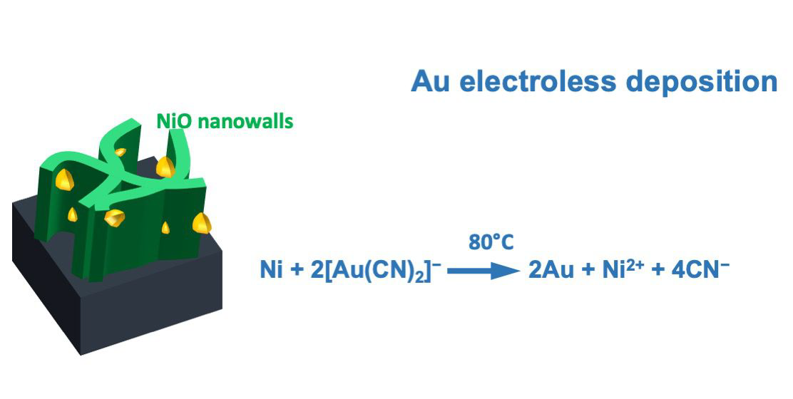
2.1. Synthesis
2.2. Characterization
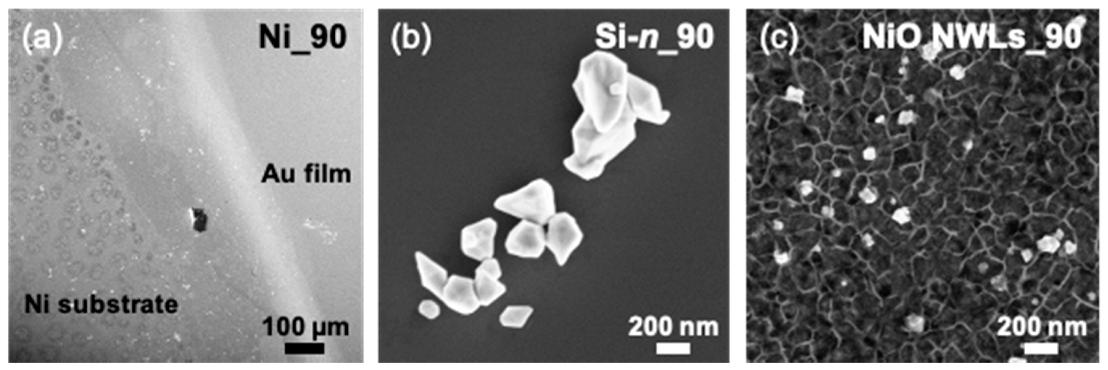
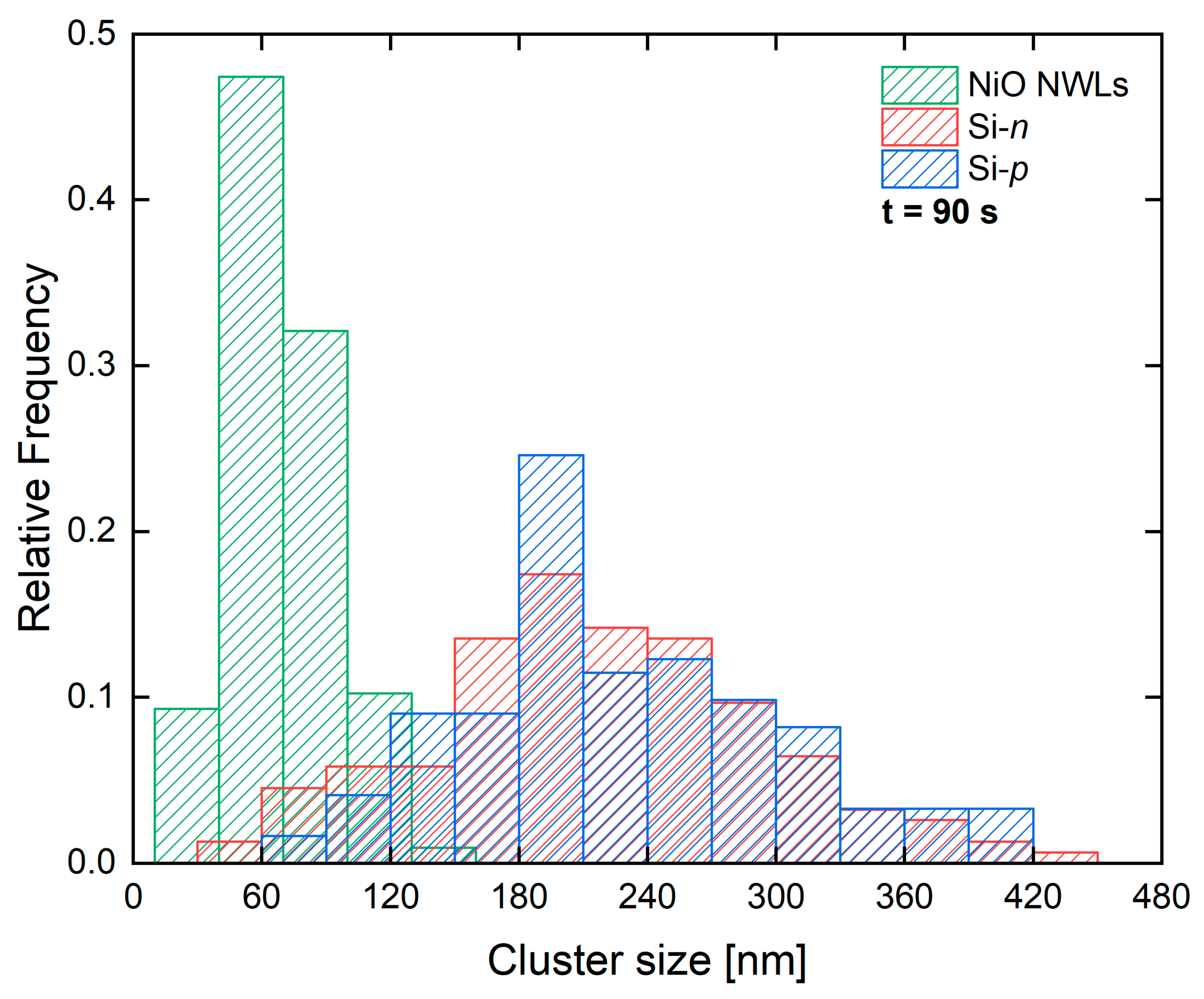
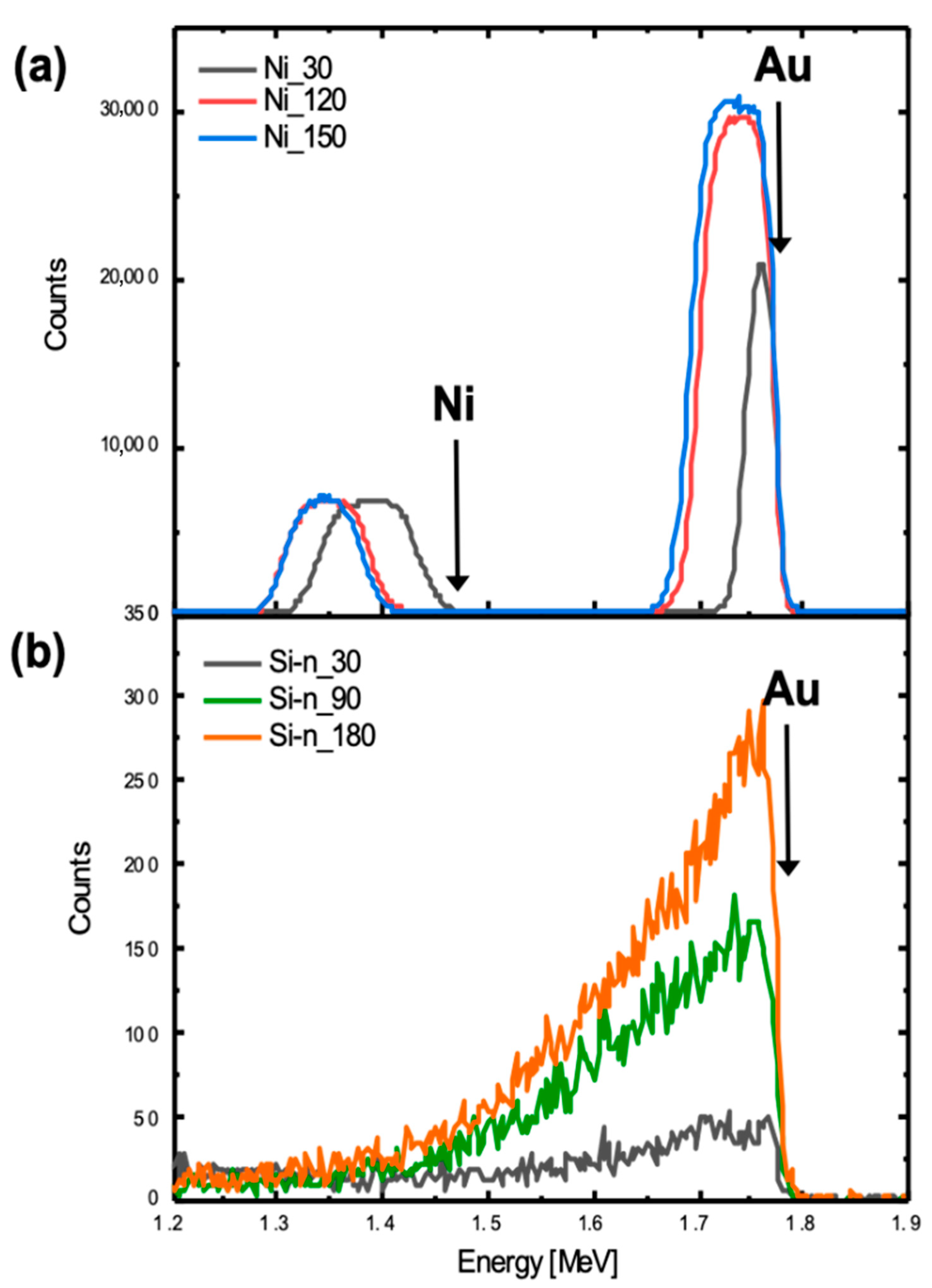
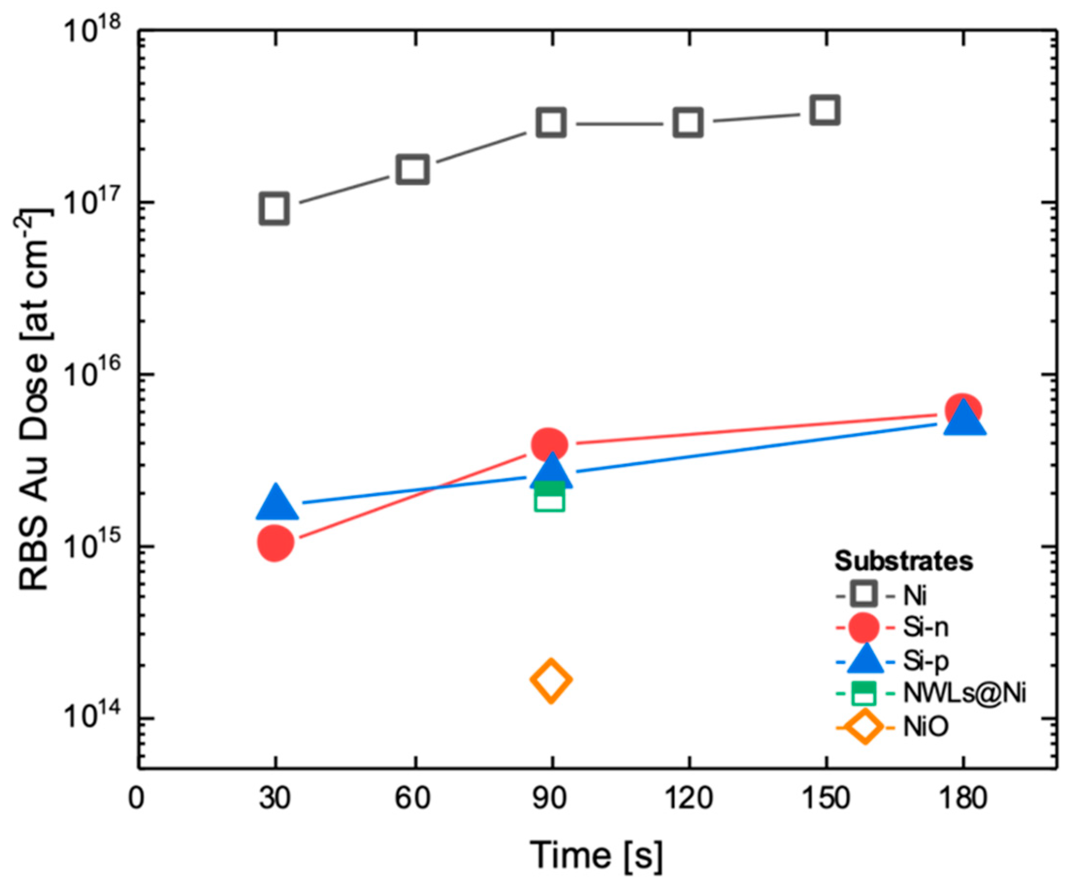
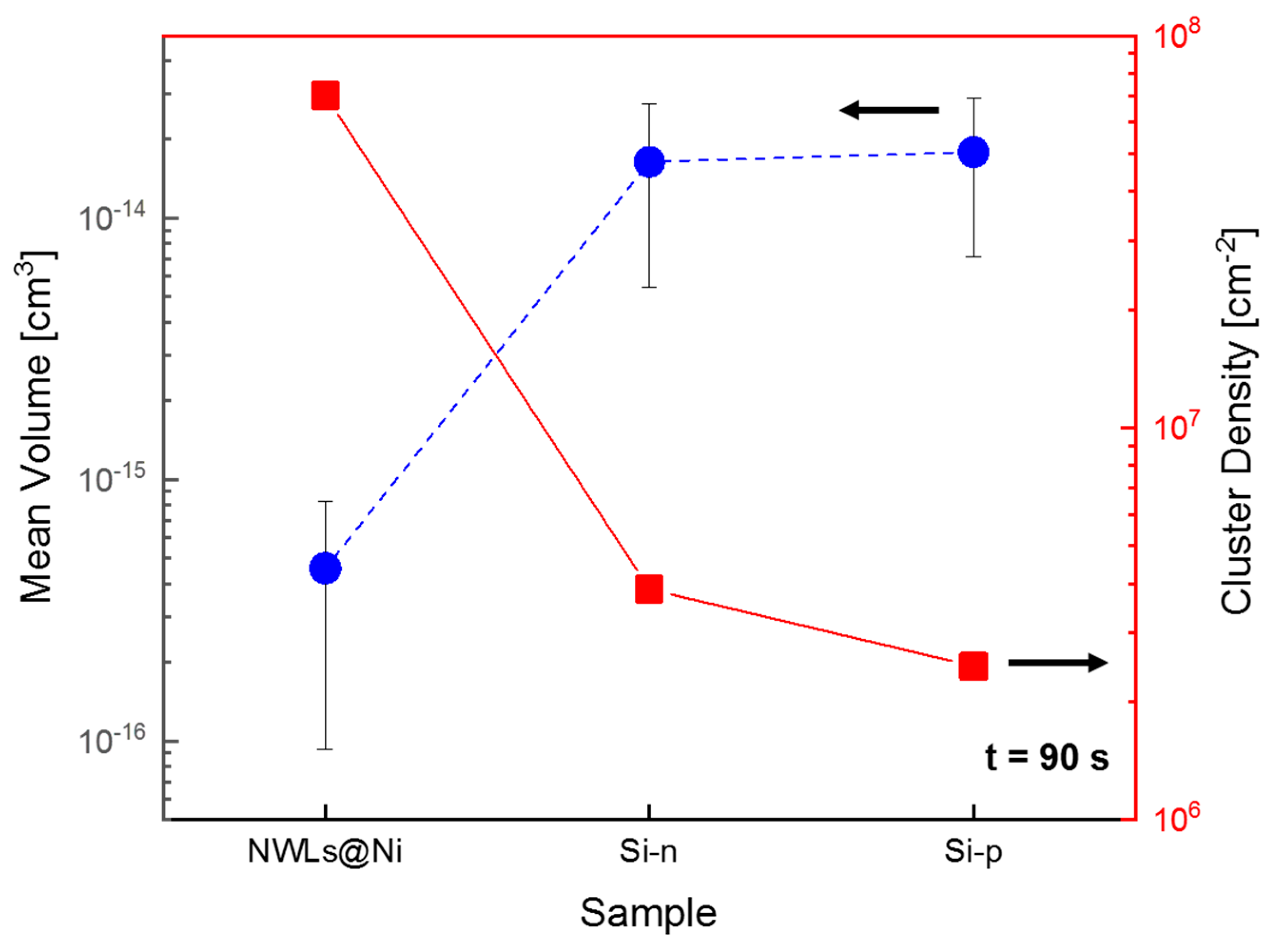
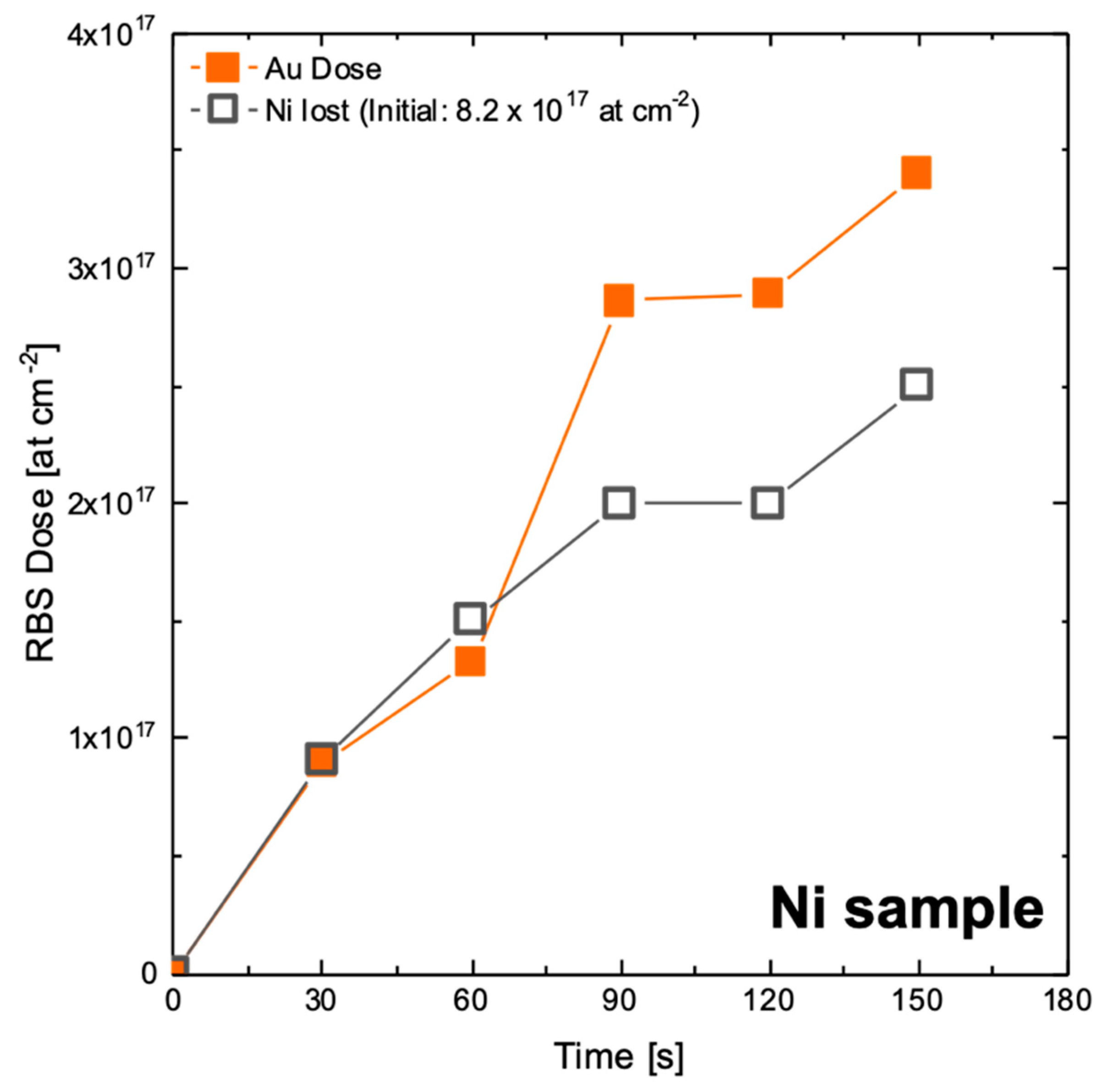
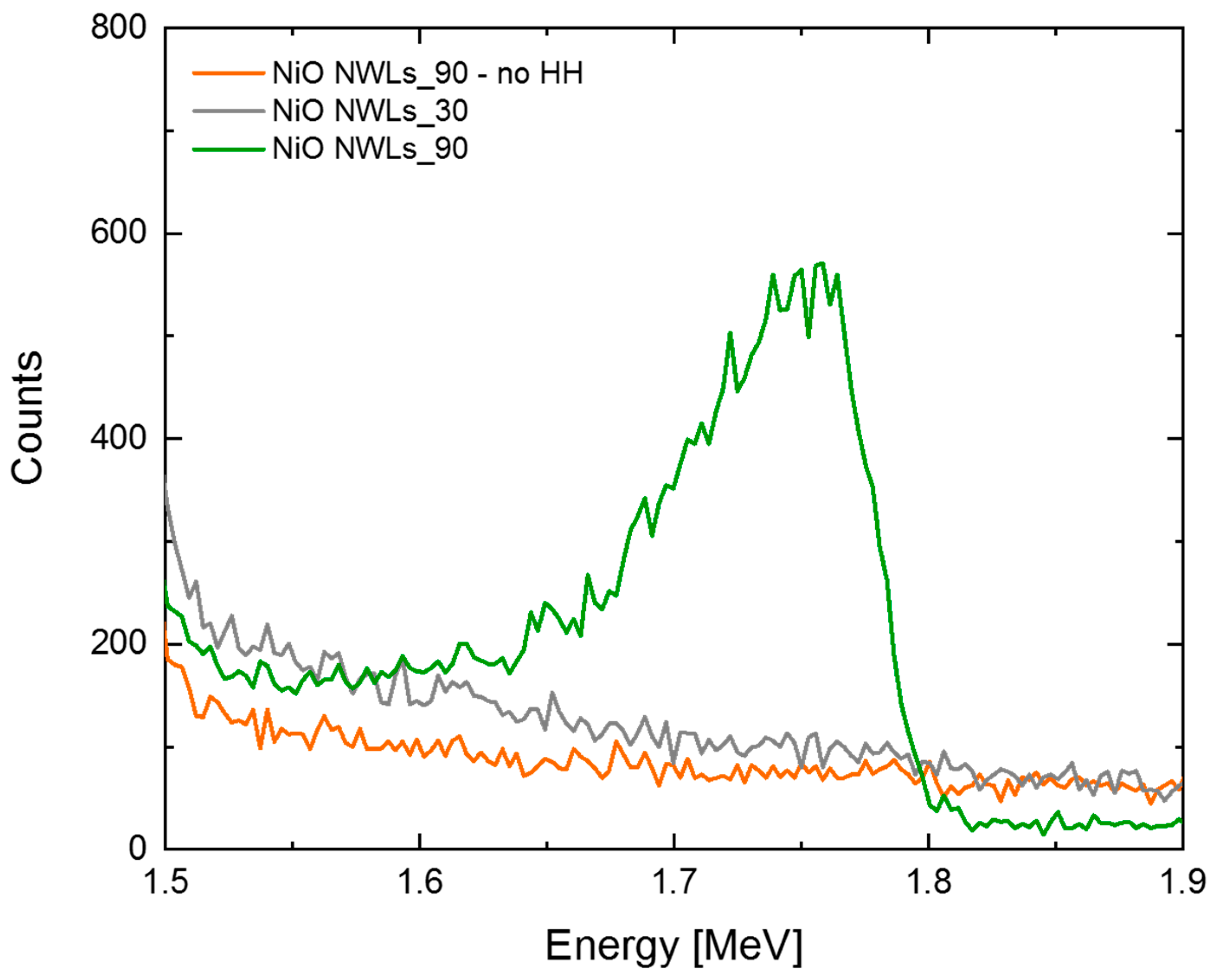
3. Results
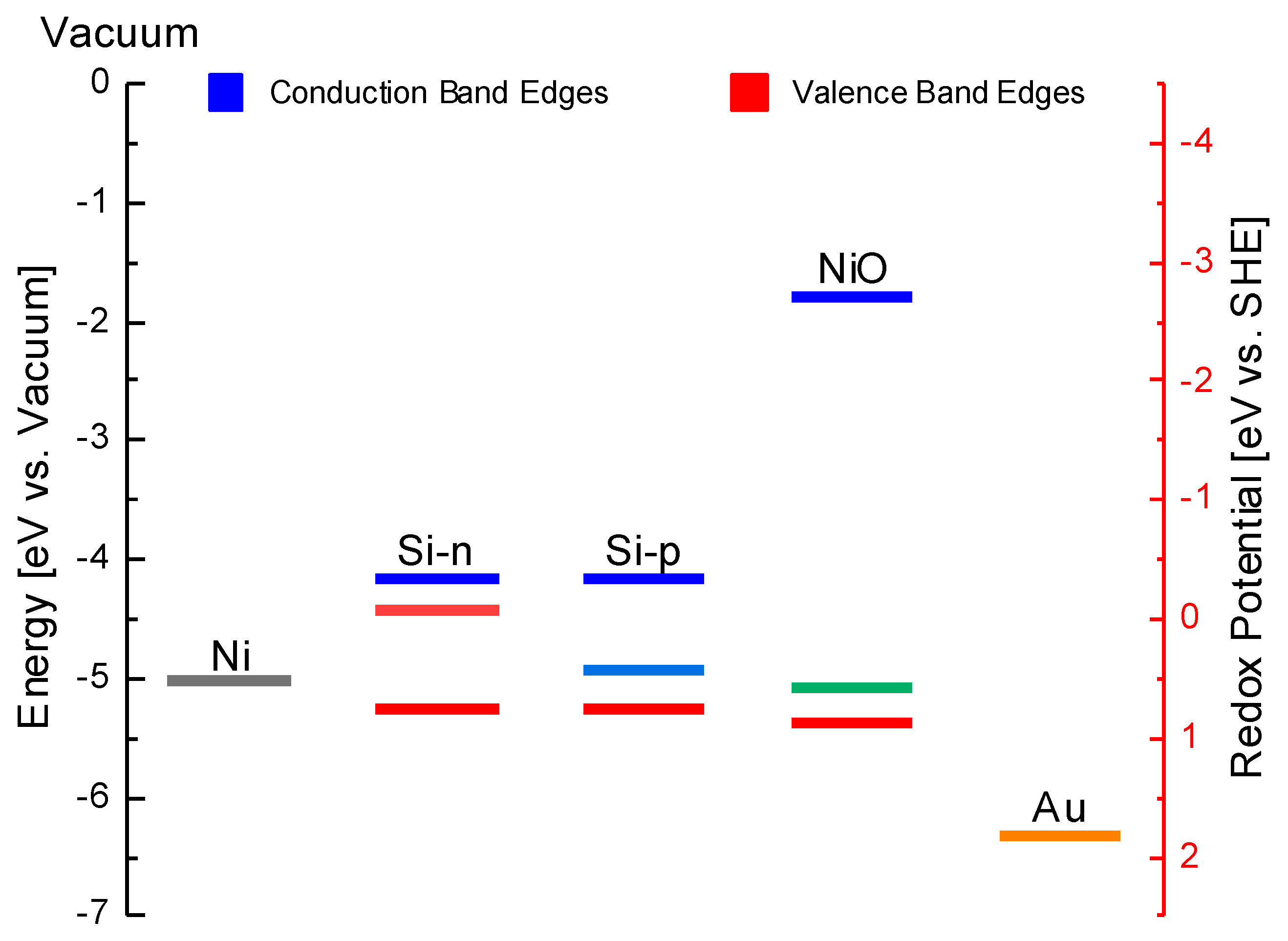
4. Discussion
5. Conclusions
Supplementary Materials
Author Contributions
Funding
Acknowledgments
Conflicts of Interest
References
- Dai, S.; Chou, J.P.; Wang, K.W.; Hsu, Y.Y.; Hu, A.; Pan, X.; Chen, T.Y. Platinum-trimer decorated cobalt-palladium core-shell nanocatalyst with promising performance for oxygen reduction reaction. Nat. Commun. 2019. [Google Scholar] [CrossRef] [PubMed]
- Ranjan, P.; Shankar, S.; Popovitz-Biro, R.; Cohen, S.R.; Kaplan-Ashiri, I.; Dadosh, T.; Shimon, L.J.W.; Višić, B.; Tenne, R.; Lahav, M.; et al. Decoration of Inorganic Nanostructures by Metallic Nanoparticles to Induce Fluorescence, Enhance Solubility, and Tune Band Gap. J. Phys. Chem. C 2018, 122, 6748–6759. [Google Scholar] [CrossRef]
- Su, S.; Xu, Y.; Sun, Q.; Gu, X.; Weng, L.; Wang, L. Noble metal nanostructures-decorated molybdenum disulfide nanocomposites: Synthesis and application. J. Mater. Chem. B 2018, 6, 5323–5334. [Google Scholar] [CrossRef] [PubMed]
- Bhardwaj, N.; Satpati, B.; Mohapatra, S. Plasmon-enhanced photoluminescence from SnO2 nanostructures decorated with Au nanoparticles. Appl. Surf. Sci. 2020, 504, 144381. [Google Scholar] [CrossRef]
- Wang, C.; Wang, T.; Wang, B.; Zhou, X.; Cheng, X.; Sun, P.; Zheng, J.; Lu, G. Design of α-Fe 2 O 3 nanorods functionalized tubular NiO nanostructure for discriminating toluene molecules. Sci. Rep. 2016. [Google Scholar] [CrossRef]
- Shi, Y.; Huang, J.K.; Jin, L.; Hsu, Y.T.; Yu, S.F.; Li, L.J.; Yang, H.Y. Selective decoration of Au nanoparticles on monolayer MoS 2 single crystals. Sci. Rep. 2013. [Google Scholar] [CrossRef]
- Walters, G.; Parkin, I.P. The incorporation of noble metal nanoparticles into host matrix thin films: Synthesis, characterisation and applications. J. Mater. Chem. 2009, 19, 574–590. [Google Scholar] [CrossRef]
- Shang, L.; Zeng, B.; Zhao, F. Fabrication of novel nitrogen-doped graphene-hollow AuPd nanoparticle hybrid films for the highly efficient electrocatalytic reduction of H2O2. ACS Appl. Mater. Interfaces 2015, 7, 122–128. [Google Scholar] [CrossRef]
- Safavi, A.; Farjami, F. Electrodeposition of gold-platinum alloy nanoparticles on ionic liquid-chitosan composite film and its application in fabricating an amperometric cholesterol biosensor. Biosens. Bioelectron. 2011. [Google Scholar] [CrossRef]
- Colombelli, A.; Manera, M.G.; Taurino, A.; Catalano, M.; Convertino, A.; Rella, R. Au nanoparticles decoration of silica nanowires for improved optical bio-sensing. Sens. Actuators B Chem. 2016, 226, 589–597. [Google Scholar] [CrossRef]
- Korotcenkov, G.; Gulina, L.B.; Cho, B.K.; Han, S.H.; Tolstoy, V.P. SnO2-Au nanocomposite synthesized by successive ionic layer deposition method: Characterization and application in gas sensors. Mater. Chem. Phys. 2011, 128, 433–441. [Google Scholar] [CrossRef]
- Hall, D.S.; Lockwood, D.J.; Bock, C.; MacDougall, B.R. Nickel hydroxides and related materials: A review of their structures, synthesis and properties. Proc. R. Soc. A Math. Phys. Eng. Sci. 2015. [Google Scholar] [CrossRef]
- Kim, S.I.; Thiyagarajan, P.; Jang, J.H. Great improvement in pseudocapacitor properties of nickel hydroxide via simple gold deposition. Nanoscale 2014, 6, 11646–11652. [Google Scholar] [CrossRef] [PubMed]
- Qu, B.; Hu, L.; Chen, Y.; Li, C.; Li, Q.; Wang, Y.; Wei, W.; Chen, L.; Wang, T. Rational design of Au-NiO hierarchical structures with enhanced rate performance for supercapacitors. J. Mater. Chem. A 2013, 1, 7023–7026. [Google Scholar] [CrossRef]
- Urso, M.; Pellegrino, G.; Strano, V.; Bruno, E.; Priolo, F.; Mirabella, S. Enhanced sensitivity in non-enzymatic glucose detection by improved growth kinetics of Ni-based nanostructures. Nanotechnology 2018, 29, 165601. [Google Scholar] [CrossRef]
- Gostin, E.L.; Swan, S.D. Method and Composition for Plating By Chemical Reduction. U.S. Patent 3,032,436, 1 May 1962. [Google Scholar]
- Ali, H.O.; Christie, I.R.A. A review of electroless gold deposition processes. Gold Bull. 1984, 17, 118–127. [Google Scholar] [CrossRef]
- Mallory, G.O.; Hajdu, J.B. Electroless Plating: Fundamentals and Applications; American Electroplaters and Surface Finishers Society: Orlando, FL, USA, 1990. [Google Scholar]
- Stojan, D. Electrodeposition—Theory and Practice. In Modern Aspects of Electrochemistry; Springer: Berlin/Heidelberg, Germany, 2010. [Google Scholar]
- Azmah Hanim, M.A. Electroless Plating as Surface Finishing in Electronic Packaging. In Comprehensive Materials Finishing; Elsevier: Amsterdam, The Netherlands, 2017; ISBN 9780128032503. [Google Scholar]
- Sudagar, J.; Lian, J.; Sha, W. Electroless nickel, alloy, composite and nano coatings—A critical review. J. Alloys Compd. 2013, 571, 183–204. [Google Scholar] [CrossRef]
- Ogata, Y.H.; Kobayashi, K.; Motoyama, M. Electrochemical metal deposition on silicon. Curr. Opin. Solid State Mater. Sci. 2006, 10, 163–172. [Google Scholar] [CrossRef]
- Yae, S.; Nasu, N.; Matsumoto, K.; Hagihara, T.; Fukumuro, N.; Matsuda, H. Nucleation behavior in electroless displacement deposition of metals on silicon from hydrofluoric acid solutions. Electrochim. Acta 2007. [Google Scholar] [CrossRef]
- Ahmad, R.; Bedük, T.; Majhi, S.M.; Salama, K.N. One-step synthesis and decoration of nickel oxide nanosheets with gold nanoparticles by reduction method for hydrazine sensing application. Sens. Actuators B Chem. 2019, 286, 139–147. [Google Scholar] [CrossRef]
- Urso, M.; Tumino, S.; Bruno, E.; Bordonaro, S.; Marletta, D.; Loria, G.R.; Avni, A.; Sacham-Diamand, Y.; Priolo, F.; Mirabella, S. Ultrasensitive Electrochemical Impedance Detection of Mycoplasma agalactiae DNA by Low-Cost and Disposable Au-Decorated NiO Nanowall Electrodes. ACS Appl. Mater. Interfaces 2020. [Google Scholar] [CrossRef] [PubMed]
- Bahariqushchi, R.; Cosentino, S.; Scuderi, M.; Dumons, E.; Tran-Huu-Hue, L.P.; Strano, V.; Grandjean, D.; Lievens, P.; Poulin-Vittrant, G.; Spinella, C.; et al. Free carrier enhanced depletion in ZnO nanorods decorated with bimetallic AuPt nanoclusters. Nanoscale 2020, 12, 19213–19222. [Google Scholar] [CrossRef]
- Ponnuvelu, D.V.; Dhakshinamoorthy, J.; Prasad, A.K.; Dhara, S.; Kamruddin, M.; Pullithadathil, B. Geometrically Controlled Au-Decorated ZnO Heterojunction Nanostructures for NO2 Detection. ACS Appl. Nano Mater. 2020, 3, 5898–5909. [Google Scholar] [CrossRef]
- Adawiyah, M.A.R.; Azlina, O.S.; Fadil, N.A.; Aisha, S.R.; Hanim, M.A. Electroless and Immersion Plating Process towards Structures and IMC Formation. Int. J. Eng. Technol. 2016, 8, 2558–2570. [Google Scholar] [CrossRef][Green Version]
- Wilkinson, P. Understanding gold plating. Gold Bull. 1986. [Google Scholar] [CrossRef]
- Okinaka, Y.; Hoshino, M. Some recent topics in gold plating for electronics applications. Gold Bull. 1998. [Google Scholar] [CrossRef]
- Vorobyova, T.N.; Poznyak, S.K.; Rimskaya, A.A.; Vrublevskaya, O.N. Electroless gold plating from a hypophosphite-dicyanoaurate bath. Surf. Coatings Technol. 2004, 176, 327–336. [Google Scholar] [CrossRef]
- Iwu, K.O.; Lombardo, A.; Sanz, R.; Scirè, S.; Mirabella, S. Facile synthesis of Ni nanofoam for flexible and low-cost non-enzymatic glucose sensing. Sens. Actuators B Chem. 2016, 224, 764–771. [Google Scholar] [CrossRef]
- Shacham-Diamand, Y.; Inberg, A.; Sverdlov, Y.; Bogush, V.; Croitoru, N.; Moscovich, H.; Freeman, A. Electroless processes for micro- and nanoelectronics. Electrochim. Acta 2003, 48, 2987–2996. [Google Scholar] [CrossRef]
- Li, Z.; Han, C.; Shen, J. Reduction of Ni2+ by hydrazine in solution for the preparation of nickel nano-particles. J. Mater. Sci. 2006, 41, 3473–3480. [Google Scholar] [CrossRef]
- ImageJ. Available online: www.imagej.nih.gov (accessed on 1 October 2019).
- Thompson, M. Xrump. Available online: www.genplot.com (accessed on 1 November 2019).
- Feldman, L.C.; Mayer, J.W.; Grasserbauer, M. Fundamentals of surface and thin film analysis. Anal. Chim. Acta 1987, 199, 288. [Google Scholar] [CrossRef]
- Vratny, F. Electroless Deposition of Gold. U.S. Patent 4,154,877, 24 October 1978. [Google Scholar]
- Liu, H.; Li, N.; Bi, S.; Li, D. Gold immersion deposition on electroless nickel substrates deposition process and influence factor analysis. J. Electrochem. Soc. 2007, 154, D662. [Google Scholar] [CrossRef]
- Bard, A.J.; Parsons, R.; Jordan, J. Standard Potentials in Aqueous Solution; Routledge: New York, NY, USA, 2017. [Google Scholar] [CrossRef]
- Michaelson, H.B. The work function of the elements and its periodicity. J. Appl. Phys. 1977, 48, 4729–4733. [Google Scholar] [CrossRef]
- Lahiri, A.; Kobayashi, S.I. Electroless deposition of gold on silicon and its potential applications: Review. Surf. Eng. 2016, 32, 321–337. [Google Scholar] [CrossRef]
- Aboelfotoh, M.O.; Cros, A.; Svensson, B.G.; Tu, K.N. Schottky-barrier behavior of copper and copper silicide on n-type and p-type silicon. Phys. Rev. B 1990, 41, 9819–9827. [Google Scholar] [CrossRef]
- Urso, M.; Torrisi, G.; Boninelli, S.; Bongiorno, C.; Priolo, F.; Mirabella, S. Ni(OH)2@Ni core-shell nanochains as low-cost high-rate performance electrode for energy storage applications. Sci. Rep. 2019. [Google Scholar] [CrossRef]
- Lany, S. Semiconducting transition metal oxides. J. Phys. Condens. Matter 2015, 27, 283203. [Google Scholar] [CrossRef]
- Sze, S.M.; Ng, K.K. Physics of Semiconductor Devices, 3rd ed.; Sze, S.M., Ng, K.K., Eds.; John Wiley & Sons: Hoboken, NJ, USA, 2007. [Google Scholar]


| Sample | Substrate | ELD Bath Immersion Time (s) |
|---|---|---|
| Ni | Ni layer | 30, 60, 90, 120, 150 |
| NiO | NiO layer | 90 |
| Si-n | n-type c-Si | 30, 90, 180 |
| Si-p | p-type c-Si | 30, 90, 180 |
| NiO NWLs | NiO nanowalls | 30, 90 |
Publisher’s Note: MDPI stays neutral with regard to jurisdictional claims in published maps and institutional affiliations. |
© 2020 by the authors. Licensee MDPI, Basel, Switzerland. This article is an open access article distributed under the terms and conditions of the Creative Commons Attribution (CC BY) license (http://creativecommons.org/licenses/by/4.0/).
Share and Cite
Bruno, L.; Urso, M.; Shacham-Diamand, Y.; Priolo, F.; Mirabella, S. Role of Substrate in Au Nanoparticle Decoration by Electroless Deposition. Nanomaterials 2020, 10, 2180. https://doi.org/10.3390/nano10112180
Bruno L, Urso M, Shacham-Diamand Y, Priolo F, Mirabella S. Role of Substrate in Au Nanoparticle Decoration by Electroless Deposition. Nanomaterials. 2020; 10(11):2180. https://doi.org/10.3390/nano10112180
Chicago/Turabian StyleBruno, Luca, Mario Urso, Yosi Shacham-Diamand, Francesco Priolo, and Salvo Mirabella. 2020. "Role of Substrate in Au Nanoparticle Decoration by Electroless Deposition" Nanomaterials 10, no. 11: 2180. https://doi.org/10.3390/nano10112180
APA StyleBruno, L., Urso, M., Shacham-Diamand, Y., Priolo, F., & Mirabella, S. (2020). Role of Substrate in Au Nanoparticle Decoration by Electroless Deposition. Nanomaterials, 10(11), 2180. https://doi.org/10.3390/nano10112180