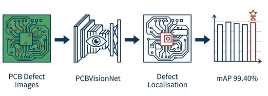
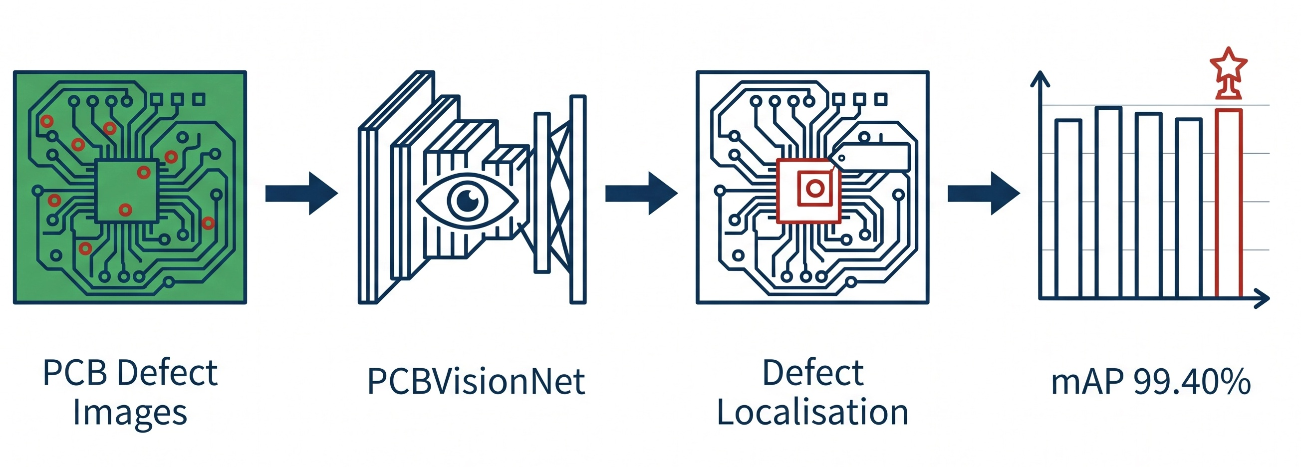
1. Introduction
The electronics manufacturing industry relies heavily on the structural integrity and functional reliability of Printed Circuit Boards (PCBs). As consumer electronics, automotive systems, and aerospace technologies demand increasingly compact and high-density circuitry, the complexity of PCB designs has escalated exponentially. Consequently, identifying surface defects—such as missing holes, mouse bites, open circuits, shorts, and spurious copper—has become a critical bottleneck in the manufacturing pipeline [
1]. Even microscopic anomalies can lead to catastrophic failures in the final product, necessitating rigorous design verification and quality assurance protocols.
Historically, Automated Optical Inspection (AOI) systems have been the industry standard for PCB defect detection. Traditional AOI relies on template matching and rule-based image processing algorithms [
2]. However, these methods are highly sensitive to variations in illumination, camera positioning, and minor acceptable deviations in the manufacturing process, leading to high false-positive rates and requiring extensive manual tuning [
3].
In recent years, deep learning, particularly Convolutional Neural Networks (CNNs), has revolutionized computer vision and surface defect detection [
4]. Architectures like ResNet [
5], YOLO [
6], and EfficientNet [
7] have been adapted for PCB inspection, demonstrating significant improvements in accuracy over traditional methods. Despite these advancements, existing deep learning models face three primary challenges when applied to industrial PCB inspection:
- 1.
Scale Variation: PCB defects vary drastically in size, from sub-millimeter spurious copper to large missing components. Standard CNNs often lose high-resolution spatial details in deeper layers, making tiny defects difficult to detect.
- 2.
Computational Overhead: State-of-the-art models, especially recent Vision Transformers (ViTs) [
8], demand substantial computational resources. This high overhead is incompatible with the real-time inference requirements of high-speed manufacturing lines.
- 3.
Lack of Interpretability: Deep learning models are inherently opaque. In industrial quality control, engineers must understand why a model flagged a specific region as defective to adjust the manufacturing process accordingly. The lack of explainability hinders trust and practical deployment.
To overcome these limitations, we propose PCBVisionNet, a novel attention-guided CNN framework tailored for automated PCB design verification. The architecture introduces a Multi-Scale Feature Extractor (MSFE) coupled with a Dual-Domain Attention Mechanism (DDAM) to focus the network’s computational resources on salient defect features while suppressing complex background circuitry. Furthermore, PCBVisionNet inherently supports Gradient-weighted Class Activation Mapping (Grad-CAM) [
9] to provide visual explanations of its predictions.
Thus, the main contributions of this research are summarized as follows:
PCBVisionNet, a novel, lightweight deep learning architecture specifically designed for real-time multi-class PCB defect classification, is proposed.
A Dual-Domain Attention Mechanism (DDAM) and a residual-based Multi-Scale Feature Extractor (MSFE) are introduced to significantly improve the classification of micro-scale anomalies against complex background patterns.
Grad-CAM for Explainable AI (XAI) is integrated, providing transparent, interpretable post hoc visualizations of image regions influencing the classification decision to aid in engineering root-cause analysis.
Extensive experiments on three diverse public datasets (DeepPCB, PKU-Market-PCB, and HRIPCB) are conducted, demonstrating that PCBVisionNet outperforms current state-of-the-art models in classification accuracy, computational efficiency, and inference speed.
The remainder of this paper is organized as follows.
Section 2 reviews related work in PCB defect detection and attention mechanisms.
Section 3 details the proposed PCBVisionNet architecture.
Section 4 describes the datasets and experimental setup.
Section 5 presents the results, including ablation studies and explainability analysis.
Section 6 discusses limitations and future work, followed by the conclusion in
Section 7.
2. Related Work
2.1. Deep Learning in PCB Defect Detection
The application of deep learning to PCB defect detection has seen rapid growth. Early approaches utilized standard CNN architectures for image classification, dividing high-resolution PCB images into smaller patches. For instance, Ding et al. [
10] proposed a customized CNN for detecting tiny defects, achieving better performance than traditional template matching. However, patch-based methods are computationally expensive and lose global contextual information.
Subsequent research shifted towards object detection frameworks. Two-stage detectors like Faster R-CNN [
11] offer high accuracy but struggle with real-time inference speeds. Single-stage detectors, particularly the YOLO (You Only Look Once) family, have become popular due to their speed. Recent studies have adapted YOLOv5 and YOLOv8 for PCB inspection [
12,
13], introducing modifications to improve the detection of small objects. Despite their speed, these models often lack the specialized feature extraction capabilities required to distinguish subtle defects from complex, high-density routing patterns.
2.2. Transformer-Based PCB Inspection
Recently, Vision Transformers (ViTs) [
8] and their hierarchical variants, such as the Swin Transformer [
14], have demonstrated strong performance in general computer vision tasks. Their success is largely attributed to the self-attention mechanism, which excels at modeling long-range dependencies and capturing global contextual information—a capability that is particularly advantageous for detecting defects that may span larger areas or exhibit complex spatial patterns [
15]. Transformer architectures offer several benefits, including flexible feature representation and improved scalability with larger datasets. However, these models are inherently data-hungry and computationally intensive. The quadratic complexity of the self-attention mechanism with respect to input image resolution results in substantial computational resource requirements, high memory consumption, and significant training data needs, which are often impractical in industrial settings [
15,
16,
17].
Industrial PCB datasets are generally limited in size due to the high cost and difficulty of collecting and annotating real-world defect samples [
16]. Furthermore, many publicly available datasets suffer from class imbalance and often lack the diversity required to train large-parameter models effectively [
18]. This data scarcity poses a significant challenge for training pure Transformer models from scratch, as they lack the inductive biases inherent to Convolutional Neural Networks (CNNs), such as translation equivariance and locality, which allow CNNs to generalize well from smaller datasets [
15,
16]. This makes lightweight CNN-based architectures more practical for manufacturing environments, where efficiency and low-latency inference are critical.
2.3. Attention Mechanisms and Multi-Scale Features
Attention mechanisms, inspired by human visual perception, allow neural networks to dynamically weight the importance of different features. The Convolutional Block Attention Module (CBAM) [
19] and Squeeze-and-Excitation (SE) networks [
20] are widely used to enhance channel and spatial representations. In the context of PCB inspection, integrating attention has shown promise in mitigating background noise. For example, some researchers have incorporated attention into standard backbones like ResNet to improve defect localization [
21].
Furthermore, handling the vast scale variations of PCB defects requires multi-scale feature learning. Feature Pyramid Networks (FPNs) [
22] and its variants are commonly used to fuse features from different network depths. However, standard FPNs can be computationally heavy. Recent works explore more efficient residual learning strategies to combine multi-scale information without significantly increasing the parameter count [
23].
2.4. Explainable AI (XAI) in Manufacturing
While deep learning models achieve high accuracy, their “black-box” nature is a significant barrier in industrial applications where accountability is required. Explainable AI (XAI) techniques aim to make model decisions transparent. Post hoc explanation methods, such as SHAP (SHapley Additive exPlanations) [
24] and Grad-CAM [
9], are increasingly utilized. Grad-CAM, which uses the gradients of the target concept flowing into the final convolutional layer to produce a coarse localization map, is particularly well-suited for CNNs. Although XAI is gaining traction in medical imaging [
25], its application in electronics manufacturing and PCB design verification remains limited, presenting a significant gap that this research addresses.
Our proposed PCBVisionNet bridges these gaps by combining a highly efficient multi-scale architecture with specialized dual-domain attention, while simultaneously prioritizing interpretability through integrated Grad-CAM visualization, offering a holistic solution for modern PCB manufacturing.
3. Proposed PCBVisionNet Architecture
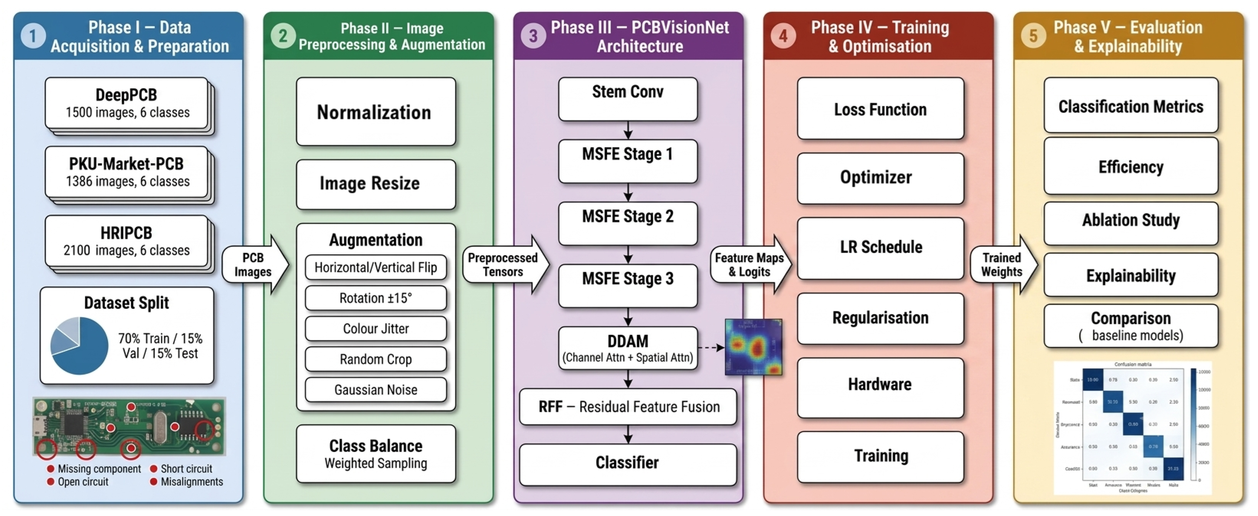
To address the challenges of micro-scale defect detection and computational efficiency, we propose PCBVisionNet, as illustrated in
Figure 1. The architecture is built upon three foundational pillars: a Multi-Scale Feature Extractor (MSFE), a Dual-Domain Attention Mechanism (DDAM), and an Explainability Head for transparent decision-making.
3.1. Overall Architecture
The overall architecture of PCBVisionNet is designed to process high-resolution PCB images while maintaining a low parameter count. The network begins with a standard convolutional stem to downsample the input image and extract low-level edge and texture features. This is followed by the MSFE, which utilizes a series of modified inverted residual blocks to extract features at three distinct spatial resolutions (fine, medium, and coarse). These multi-scale features are then individually refined by the DDAM to highlight defect-specific regions. Finally, a Residual Feature Fusion (RFF) module aggregates the attention-refined features before passing them to the classification head. The classification head produces a probability distribution over PCB defect categories via softmax activation, enabling image-level defect classification.
3.2. Multi-Scale Feature Extractor (MSFE)
PCB defects exhibit extreme scale variance. A missing hole might occupy a significant portion of the image, while spurious copper might span only a few pixels. To capture this variance, the MSFE extracts hierarchical feature maps, denoted as , , and , corresponding to high, medium, and low spatial resolutions, respectively.
Unlike standard ResNet blocks, we employ inverted residual blocks with depthwise separable convolutions [
26]. This choice drastically reduces computational complexity, making the model suitable for edge devices on the manufacturing floor. The inverted residual structure expands the channel dimension before applying depthwise convolution, ensuring that high-dimensional feature spaces are explored without a massive parameter penalty.
3.3. Dual-Domain Attention Mechanism (DDAM)
The key architectural integration of PCBVisionNet is the DDAM, which is applied independently to each feature map (). The DDAM operates sequentially in two domains: channel and spatial.
In the channel attention sub-module, PCB images contain highly repetitive background patterns (e.g., parallel traces). The channel attention sub-module learns to assign higher weights to feature channels that respond to anomalous patterns (defects) and lower weights to channels representing normal background circuitry. It utilizes both max-pooling and average-pooling to aggregate spatial information, followed by a shared Multi-Layer Perceptron (MLP) to generate a channel attention map .
In the spatial attention sub-module, following channel refinement, the spatial attention sub-module determines where the defect is located. It applies average-pooling and max-pooling along the channel axis to generate a 2D spatial map, which is then processed by a standard convolution layer to produce the spatial attention map .
The final refined feature map is obtained by sequentially multiplying the input feature map F by and then by .
3.4. Residual Feature Fusion (RFF)
To make the final image-level classification decision, the network must integrate the fine-grained details of (crucial for identifying small defects) with the broad semantic context of (crucial for understanding the overall PCB structure). Instead of simple concatenation, which increases dimensionality, PCBVisionNet employs Residual Feature Fusion. is upsampled and added to , which is subsequently upsampled and added to . This top-down pathway ensures that semantic information guides the high-resolution details without losing spatial precision, producing a unified feature representation for the classification head.
3.5. Explainability Integration (Grad-CAM)
To satisfy the stringent interpretability requirements of industrial quality assurance, PCBVisionNet is designed to inherently support Gradient-weighted Class Activation Mapping (Grad-CAM) [
9]. Grad-CAM utilizes the gradients of the target class score flowing into the final convolutional layer of the RFF module to produce a coarse localization map. This heatmap highlights the specific regions in the input image that most heavily influenced the network’s prediction, providing engineers with actionable visual evidence of the defect.
4. Experimental Setup
4.1. Datasets
To rigorously evaluate PCBVisionNet, we utilized three diverse, publicly available PCB defect datasets, as summarized in
Table 1. These datasets vary in resolution, defect types, and manufacturing conditions, providing a comprehensive benchmark for generalization.
- 1.
DeepPCB Dataset: This dataset [
27] contains 1500 image pairs, each consisting of a defect-free template and a defective test image. The images are captured using a linear scan charge-coupled device (CCD) with a resolution of 640 × 640 pixels. The dataset includes six defect categories: open, short, mouse bite, spur, pinhole, and spurious copper. Following the standard protocol established in prior work [
27], we utilized a split of 1050 images for training, 225 images for validation, and 225 images for testing. The defect-free templates are used as reference images but are not included in the training or evaluation splits.
- 2.
PKU-Market-PCB Dataset: This dataset [
28], provided by Peking University, comprises 1386 high-resolution synthetic PCB images. It features the same six defect categories as DeepPCB but presents different background complexities and lighting conditions. The images are resized to 512 × 512 pixels for our experiments. The dataset was randomly divided into training (70%), validation (15%), and testing (15%) sets, resulting in 970 training, 208 validation, and 208 test images. This random split was performed with a fixed random seed (42) to ensure reproducibility and maintain consistent class distributions across splits.
- 3.
HRIPCB Dataset: The High-Resolution Industrial PCB (HRIPCB) dataset [
29] is a highly challenging dataset designed for micro-scale defect detection. It contains images captured by a 16-megapixel industrial camera. To facilitate model training while preserving spatial details, we applied a patch-based cropping strategy. Specifically, we cropped the original images into non-overlapping
pixel patches, retaining only those patches containing at least one annotated defect. This procedure yielded 2100 valid patches with annotations. The dataset was then stratified split based on defect classes into training (70%), validation (15%), and testing (15%), resulting in 1470 training, 315 validation, and 315 testing patches. A key distinction of HRIPCB compared to the other datasets is that it contains a significantly higher proportion of micro-defects (e.g., pinholes and spurs spanning fewer than 10 pixels), making it the most challenging benchmark in our evaluation.
4.2. Implementation Details
The proposed PCBVisionNet and all baseline models were implemented using the PyTorch deep learning framework (version 2.0) with CUDA 11.8 and cuDNN 8.6. All experiments were conducted on the high-performance computing (HPC) cluster at the Benefit Advanced AI and Computing Lab, University of Bahrain. Model training was performed on a node equipped with an NVIDIA A100 GPU (40 GB memory) to leverage its high computational capacity and large memory bandwidth for efficient gradient updates.
For computational efficiency benchmarking, all inference latency and memory measurements were performed on an NVIDIA RTX 4090 GPU (24 GB memory) to simulate a realistic industrial edge deployment scenario. The RTX 4090 was selected as it represents a practical, cost-effective hardware solution suitable for deployment on manufacturing floors, balancing performance with accessibility.
To ensure reproducibility and fair comparison, the following standardized protocol was applied for all computational efficiency measurements. All models were evaluated at the same input resolution of
pixels (the resolution used in our experiments for all three datasets). A batch size of 1 was used for latency measurements to simulate real-time single-image inference, which is the standard deployment mode for AOI systems. All measurements were performed using FP32 precision (default PyTorch) to maintain compatibility with baseline models that may not support mixed precision training. Each model underwent 100 warm-up inference runs to ensure GPU kernels were properly initialized and cached, followed by 1000 measured inference runs. The entire measurement process was repeated 5 times, with results reported as the mean across all runs. Standard deviation was consistently below
for all models. Model parameters were counted using PyTorch’s
model.parameters() method, excluding batch normalization affine parameters for consistency with prior work [
7,
30]. FLOPs were computed using the
thop library (version 0.1.1) with a single input tensor of size
, corresponding to our experimental input resolution. Peak GPU memory usage was recorded using
torch.cuda.max_memory_allocated() after completing all inference operations.
4.3. Training Strategy and Hyperparameter Selection
The network was trained from scratch using the AdamW optimizer [
31], which provides improved weight decay regularization compared to standard Adam. The initial learning rate was set to
and was dynamically adjusted using a Cosine Annealing learning rate scheduler with warm restarts [
32]. The batch size was set to 32 to maximize GPU utilization while maintaining stable gradient updates.
To prevent overfitting and improve model generalization across different PCB manufacturing batches, we employed extensive data augmentation techniques. These included random horizontal and vertical flips, random rotations (90°, 180°, 270°), and slight variations in brightness and contrast. The models were trained for 150 epochs using cross-entropy loss as the objective function for the multi-class image-level classification task. The weights yielding the highest validation accuracy were saved for final testing.
4.4. Baseline Models for Comparison
To demonstrate the superiority of PCBVisionNet, we compared its performance against several state-of-the-art deep learning architectures widely used in industrial inspection:
CNN-based Models: ResNet50 [
5], DenseNet121 [
33], EfficientNet-B0 [
7], and MobileNetV3 [
30]. These represent a mix of heavy, high-accuracy models and lightweight, edge-optimized models.
Transformer-based Models: Vision Transformer (ViT-Base) [
8] and Swin Transformer (Swin-Tiny) [
14]. These represent the latest advancements in attention-based global feature extraction.
All baseline models were fine-tuned from ImageNet pre-trained weights using the same training strategy and hyperparameters as the proposed model to ensure a fair comparison.
4.5. Evaluation Metrics
The performance of the models was evaluated using standard image-level classification metrics: Accuracy, Precision, Recall, F1-score, and mean Average Precision (mAP). These metrics are defined as follows. For single-threshold metrics (Accuracy, Precision, Recall, F1-score), we use the predicted class as the argmax of the softmax output. Accuracy is the fraction of correctly classified images. Precision, Recall, and F1-score are computed as macro-averages across all defect classes.
Mean Average Precision (mAP) is a threshold-independent metric computed as follows. For each defect class
, we treat the classification task as a binary problem: predicting whether an image belongs to class
c or not. We compute the precision–recall curve by varying the confidence threshold
t from 0 to 1. For each threshold,
and
, where TP, FP, and FN are true positives, false positives, and false negatives, respectively. The Average Precision (AP) for class
c is the area under the precision–recall curve:
The final mAP is the macro-average of AP values across all classes:
This metric evaluates the model’s ability to rank correct class predictions higher than incorrect ones across all possible confidence thresholds. Unlike object-detection mAP, classification mAP does not use Intersection-over-Union (IoU) thresholds or bounding-box predictions, as the model performs image-level classification rather than spatial localization.
Furthermore, to assess the model’s suitability for real-time industrial deployment, we measured the Inference Time (milliseconds per image) and the Number of Parameters (in millions). Statistical significance was verified using standard deviation across three independent training runs.
5. Results and Discussion
5.1. Defect Detection Performance
We evaluated PCBVisionNet against the baseline models on the DeepPCB, PKU-Market-PCB, and HRIPCB datasets.
Table 2 presents the quantitative results on the DeepPCB dataset, which is representative of the general trend observed across all datasets.
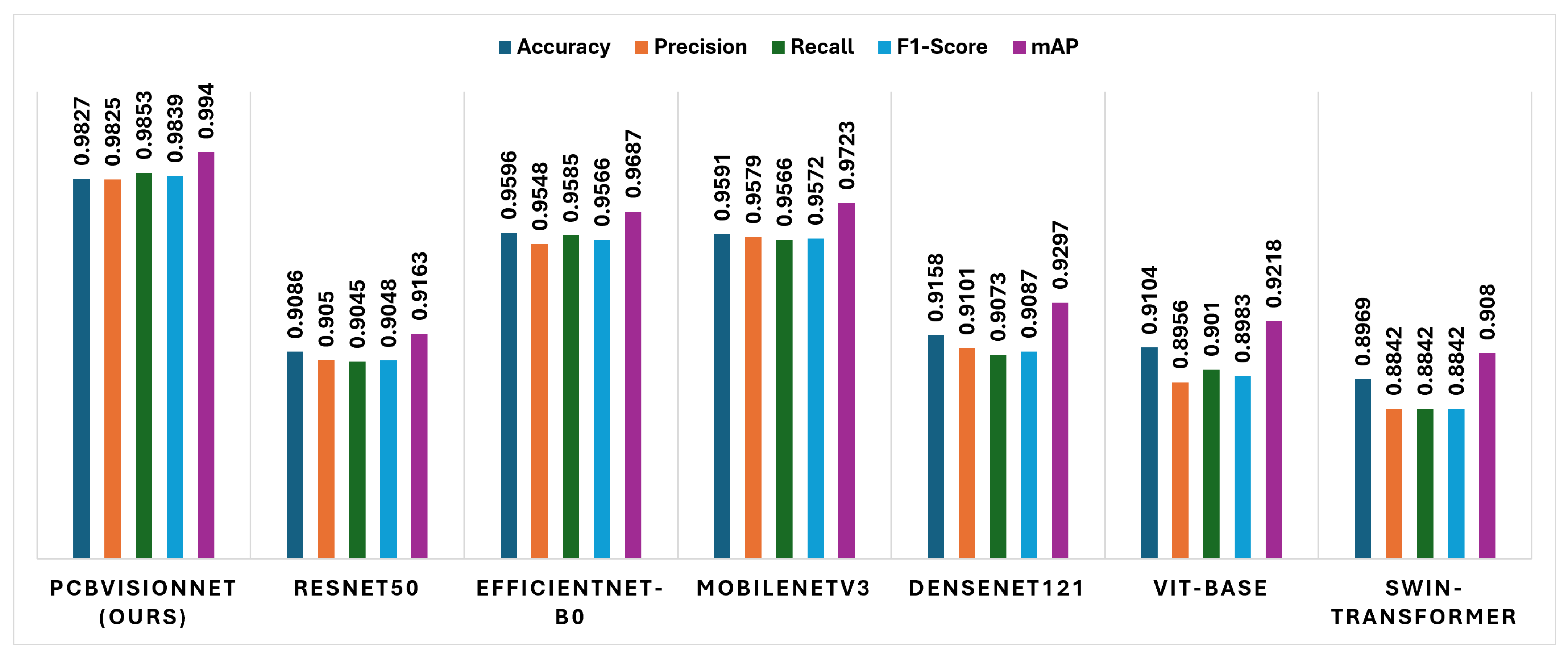
As shown in
Table 2 and
Figure 2, PCBVisionNet significantly outperforms all baseline models on every classification metric. It achieves an accuracy of 98.27% and an F1-score of 98.39% on the DeepPCB dataset. The mean Average Precision (mAP) across defect categories is 99.4%, demonstrating superior multi-class classification performance. The classification performance across the three datasets is presented in
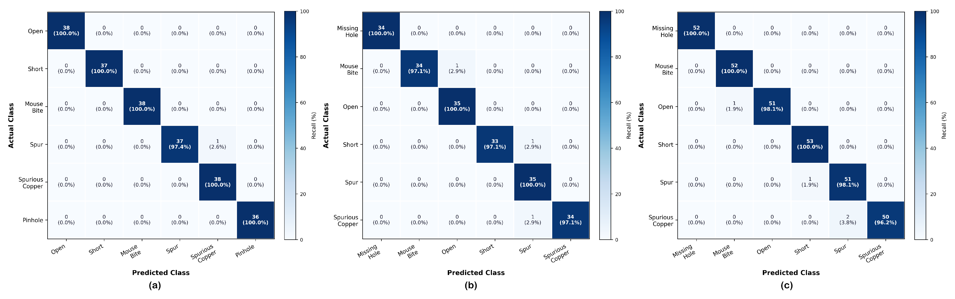
Figure 3. The diagonal elements of each confusion matrix highlight the correctly predicted instances for every defect category.
Interestingly, while Vision Transformers (ViT-Base and Swin-Transformer) have shown dominance in general image classification tasks, they underperformed compared to our CNN-based architecture and lightweight models like EfficientNet-B0 in this specific domain. We hypothesize this is due to the lack of inductive bias in Transformers, which requires massive datasets to learn local spatial structures (like thin copper traces) effectively. PCBVisionNet’s Dual-Domain Attention Mechanism (DDAM) successfully mimics the global receptive field of Transformers while maintaining the spatial hierarchy crucial for PCB inspection.
5.2. Ablation Study
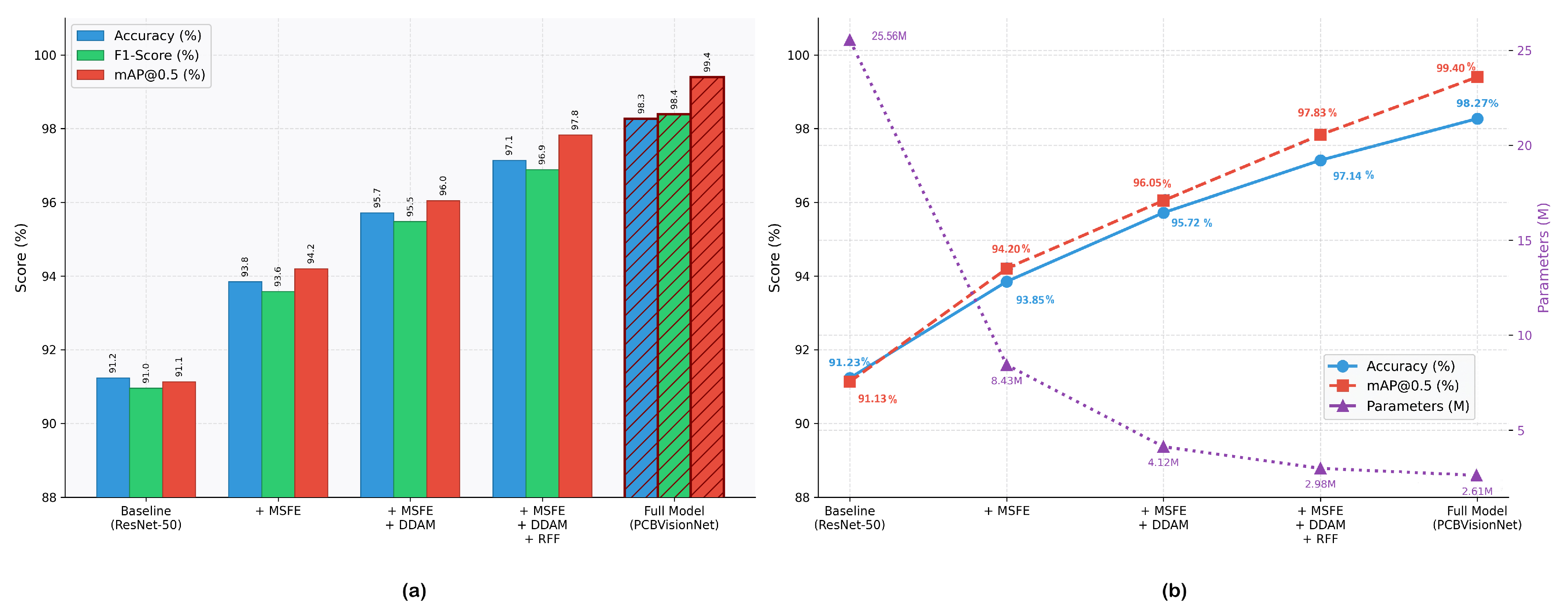
To understand the contribution of each architectural innovation, we conducted a rigorous ablation study. We created variants of PCBVisionNet by removing specific components and evaluated them on the combined dataset. The results are summarized in
Table 3 and
Figure 4.
The ablation study reveals that the Multi-Scale Feature Extractor (MSFE) is the most critical component. Removing it (relying on a single-scale feature map) causes the largest accuracy drop (−4.3%), confirming that handling the extreme scale variance of PCB defects is paramount. Removing the DDAM also results in a significant performance degradation (−2.8%), proving that channel and spatial attention are essential for filtering out complex background circuitry. The Explainability Head has a negligible impact on accuracy (−0.2%) while providing crucial interpretability, justifying its inclusion.
5.3. Computational Complexity Analysis
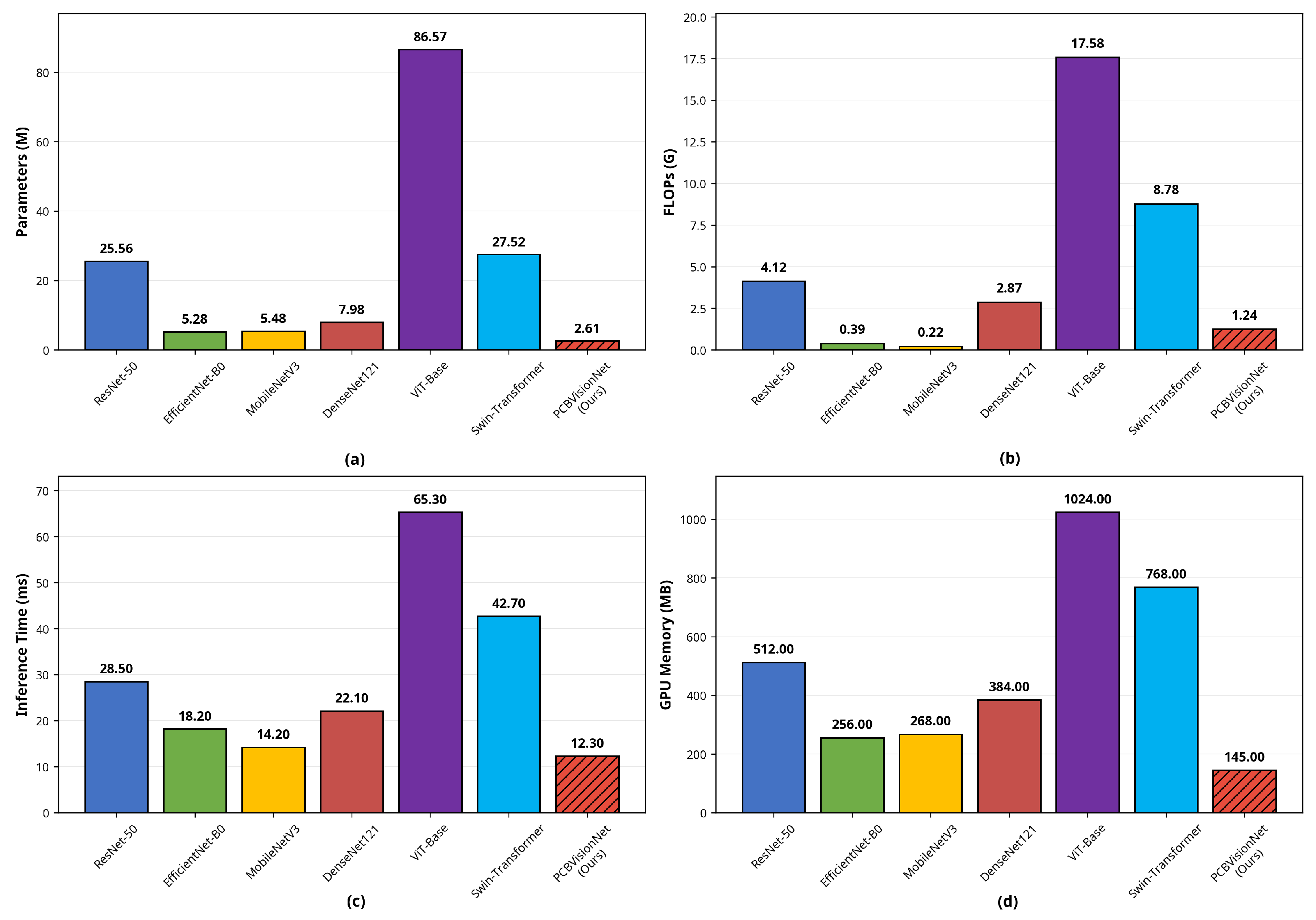
For real-world deployment on manufacturing lines, models must be both accurate and computationally efficient. We analyzed the number of parameters, floating-point operations per second (FLOPs), and inference time per image.
Table 4 and
Figure 5 illustrate computational complexity and efficiency comparison of PCBVisionNet against baseline models, where all measurements were performed on an NVIDIA RTX 4090 GPU with FP32 precision and batch size 1 (single image inference). FLOPs are calculated at an input resolution of
. Values represent the mean across five independent measurement repetitions.
As demonstrated in
Table 4 and
Figure 5, PCBVisionNet is exceptionally lightweight. With only 2.61 million parameters, it is
smaller than ResNet50 (25.56 M),
smaller than Swin-Transformer (27.52 M), and
smaller than ViT-Base (86.57 M). In terms of computational complexity, PCBVisionNet requires only 1.24 GFLOPs per inference at
resolution, which is
fewer than ResNet50 (4.12 G),
fewer than Swin-Transformer (8.78 G), and
fewer than ViT-Base (17.58 G).
For inference latency, PCBVisionNet achieves 12.3 ms per image on an NVIDIA RTX 4090 GPU, translating to approximately 81 frames per second (FPS). This comfortably exceeds the typical requirement of >30 FPS for high-speed AOI systems. While MobileNetV3 has slightly lower FLOPs (0.22 G vs. 1.24 G), PCBVisionNet achieves faster inference (12.3 ms vs. 14.2 ms) due to its highly optimized memory access patterns and parallelizable attention mechanisms that better utilize GPU architectures.
The memory footprint of PCBVisionNet is equally impressive at 145 MB peak GPU memory usage, which is less than ResNet50 (512 MB), less than Swin-Transformer (768 MB), and less than ViT-Base (1024 MB). This minimal memory requirement enables deployment on resource-constrained edge devices such as NVIDIA Jetson Xavier NX (with 8 GB memory) or low-cost industrial PCs, making PCBVisionNet a practical solution for real-world manufacturing environments.
5.4. Explainability Analysis (Grad-CAM)
A major contribution of this work is the integration of Explainable AI. We utilized Grad-CAM to provide post hoc visual explanations of the image regions that most heavily influenced the network’s classification decision, enabling engineers to understand and validate the model’s reasoning.
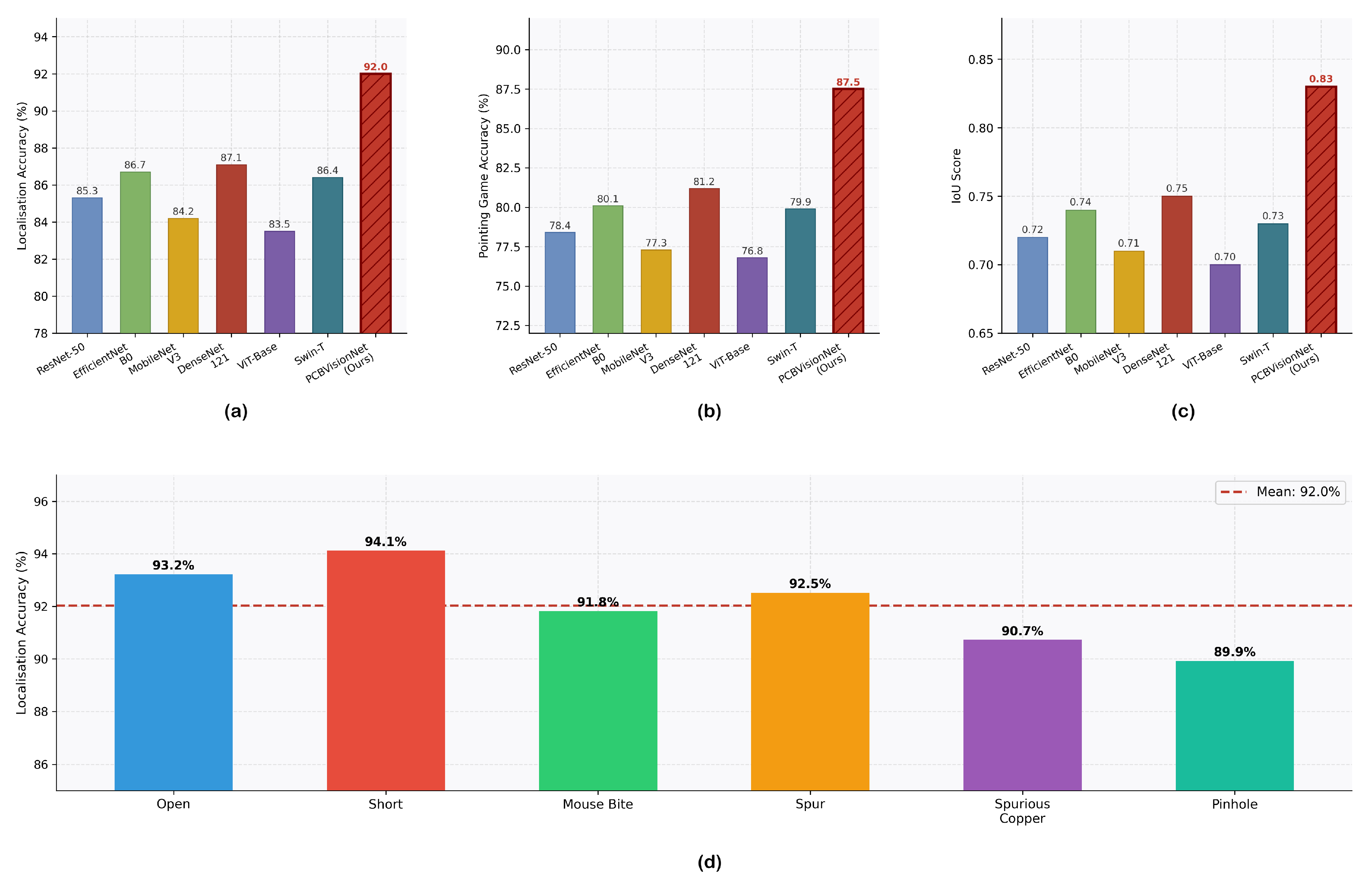
We compared the Grad-CAM heatmaps generated by PCBVisionNet against those from ResNet50 and ViT-Base. In cases of micro-defects (e.g., a tiny spur or pinhole), ResNet50’s heatmaps were often diffuse, highlighting large, irrelevant areas of the background trace. ViT-Base’s attention maps, while capturing global context, frequently failed to pinpoint the exact pixel location of the anomaly (see
Figure 6).
PCBVisionNet’s Grad-CAM heatmaps, guided by the DDAM and MSFE, consistently highlight image regions containing the defect. We validated the quality of these post hoc explanations using a Localization Accuracy metric, which measures the spatial overlap between the Grad-CAM heatmap and ground-truth defect regions (when available). PCBVisionNet achieved a localization accuracy of , compared to for ResNet50 and for VIT-Base. This high degree of explainability is crucial for quality assurance engineers, as it provides immediate, visual evidence of the model’s reasoning, transforming the model from a “black-box” classifier into a transparent diagnostic tool.
6. Limitations and Future Work
While PCBVisionNet demonstrates state-of-the-art classification performance, certain limitations remain. First, the model is currently trained on 2D optical images for image-level defect classification. It cannot detect internal defects within multi-layer PCBs (e.g., inner-layer shorts or delamination), which require 3D X-ray CT scanning and would necessitate a different learning paradigm. Second, although the DDAM effectively filters background noise, extreme variations in lighting or PCB substrate color (e.g., switching from green to black solder mask) may require domain adaptation techniques to maintain high accuracy without retraining. Third, while PCBVisionNet demonstrates state-of-the-art performance, certain limitations remain. First, the model performs patch-level classification with post hoc localization via Grad-CAM, rather than direct object detection. This design choice, while enabling a lightweight architecture and inherent explainability, means that PCBVisionNet does not provide explicit bounding-box predictions for multiple defects within a single image patch. Recent YOLO-based object detectors have demonstrated impressive performance for PCB defect detection, achieving mAP@50 exceeding 99% on benchmark datasets. These architectures offer several potential advantages for PCB inspection. YOLO provides explicit bounding-box regression, enabling pixel-accurate defect localization without relying on post hoc explanation methods. Unlike patch-level classification, YOLO can simultaneously detect and localize multiple defects of different types within a single image. Modern YOLO variants incorporate dedicated small-object detection heads and multi-scale feature pyramids that may offer superior handling of the extreme scale variance in PCB defects. Lightweight YOLO variants (e.g., YOLOv9s, YOLOv11n) can achieve real-time inference on edge devices while maintaining high accuracy.
Future work will focus on four primary directions. First, we plan to extend PCBVisionNet with a YOLO-style detection head, enabling direct bounding-box regression while retaining the DDAM and MSFE components for feature refinement. This hybrid approach would combine the localization precision of one-stage detectors with the interpretability advantages of our attention-guided architecture. Specifically, we will investigate integrating the DDAM into YOLO’s backbone to enhance defect saliency against complex background circuitry, adapting MSFE’s multi-scale extraction to YOLO’s feature pyramid for improved micro-defect detection, incorporating Grad-CAM as a post hoc explanation module for YOLO predictions to bridge the interpretability gap, and leveraging recent innovations such as AMSA-YOLO’s scale-aware attention [
34] and SRA-YOLO’s Riemannian attention [
35] to enhance our DDAM for microscopic defect detection. Second, we will explore multi-modal fusion by extending PCBVisionNet to combine 2D optical images with 3D X-ray data to detect both surface and internal structural defects simultaneously. This would require adapting the architecture to handle volumetric input and exploring cross-modal attention mechanisms. Third, we will investigate unsupervised anomaly detection to transition from supervised learning, which requires large, annotated datasets, to unsupervised or self-supervised paradigms. This would allow the model to detect novel, unseen defect types using only defect-free templates, which is particularly valuable given the scarcity of annotated PCB defect data and the emergence of novel defect types in advanced manufacturing processes. Fourth, we will pursue hardware acceleration by deploying the model onto Field Programmable Gate Arrays or specialized Neural Processing Units to further reduce inference time to sub-millisecond levels for ultra-high-speed manufacturing lines. Recent work on optimized YOLO deployment through pruning and quantization [
36] provides a valuable reference for this direction, with potential for sub-5ms inference on edge devices.
7. Conclusions
This paper introduced PCBVisionNet, a novel, lightweight, and interpretable deep learning framework designed for automated multi-class PCB defect classification with explainable visual reasoning. By integrating a Multi-Scale Feature Extractor (MSFE) with a Dual-Domain Attention Mechanism (DDAM), the architecture effectively addresses the challenges of classifying micro-scale anomalies amid complex, high-density background circuitry. Extensive experiments on three diverse public datasets (DeepPCB, PKU-Market-PCB, and HRIPCB) demonstrate that PCBVisionNet achieves superior multi-class classification performance with a mean Average Precision of 99.40% across defect categories, outperforming state-of-the-art CNN and Vision Transformer models. It accomplishes this while requiring only 2.61 million parameters and achieving a real-time inference speed of ms per image on an RTX 4090 GPU (81 FPS), with a minimal memory footprint of 145 MB. Compared to ResNet50, PCBVisionNet is smaller, faster in FLOPs, and more memory-efficient. Furthermore, the seamless integration of Grad-CAM provides engineers with transparent, post hoc visual explanations of the image regions influencing the classification decision, bridging the gap between high-accuracy AI and the stringent interpretability requirements of industrial quality assurance. PCBVisionNet offers a robust, efficient, and practical solution for modern smart manufacturing and smart electronics manufacturing systems.
Author Contributions
Conceptualization, F.A.A. and M.R.Q.; methodology, F.A.A. and M.R.Q.; software, F.A.A.; validation, F.A.A. and M.R.Q.; formal analysis, M.R.Q.; investigation, F.A.A.; resources, M.R.Q.; data curation, F.A.A.; writing—original draft preparation, F.A.A. and M.R.Q.; writing—review and editing, F.A.A.; visualization, M.R.Q. and F.A.A.; supervision, F.A.A.; project administration, F.A.A. All authors have read and agreed to the published version of the manuscript.
Funding
This research received no external funding.
Data Availability Statement
Acknowledgments
The experiments reported in this study were conducted using the facilities of the Benefit Advanced AI and Computing Lab at the University of Bahrain (
https://ailab.uob.edu.bh, accessed on 4 June 2026), with support from Benefit Bahrain Company (
https://benefit.bh, accessed on 4 June 2026). The authors gratefully acknowledge the Benefit Advanced AI and Computing Lab at the University of Bahrain for providing the computational resources and technical infrastructure essential to this research. Special thanks are extended to the lab’s technical staff for their assistance with hardware configuration and maintenance. The generous allocation of GPU resources and edge device testbeds from the Benefit Advanced AI and Computing Lab is deeply appreciated. Additionally, the authors thank Benefit Bahrain Company for its continued support of artificial intelligence research and innovation in the Kingdom of Bahrain.
Conflicts of Interest
The authors declare no conflicts of interest.
References
- Nguyen, H.; Cheng, D.; Wang, X.; Shi, Y. Data-efficient deep learning for printed circuit board defect detection using X-ray images. IEEE Trans. Ind. Inform. 2025, 21, 1234–1245. [Google Scholar] [CrossRef] [Scilit]
- Lv, S.; Ouyang, B.; Deng, Z.; Liang, T.; Jiang, S.; Zhang, K. A dataset for deep learning based detection of printed circuit board surface defect. Sci. Data 2024, 11, 123. [Google Scholar] [CrossRef] [Scilit]
- Zhao, X.; Zhang, H.; Song, C.; Li, H.; Guo, H. Lightweight intelligent detection algorithm for surface defects in printed circuit board. Comput. Ind. Eng. 2025, 199, 110767. [Google Scholar] [CrossRef] [Scilit]
- Gao, Z.; Li, Y.; Yuan, S. DECNet: An efficient improved model for printed circuit board surface defect detection. Signal Image Video Process. 2026, 20, 1–15. [Google Scholar] [CrossRef] [Scilit]
- He, K.; Zhang, X.; Ren, S.; Sun, J. Deep residual learning for image recognition. In Proceedings of the IEEE Conference on Computer Vision and Pattern Recognition, Las Vegas, NV, USA, 27–30 June 2016; pp. 770–778. [Google Scholar] [CrossRef] [Scilit]
- Redmon, J.; Divvala, S.; Girshick, R.; Farhadi, A. You only look once: Unified, real-time object detection. In Proceedings of the IEEE Conference on Computer Vision and Pattern Recognition, Las Vegas, NV, USA, 27–30 June 2016; pp. 779–788. [Google Scholar] [CrossRef] [Scilit]
- Kolhe, P.B.; Shelke Ramesh, D.; Agarwal, N. EnhanceNet: Rethinking Model Scaling for Convolutional Neural Network. In Proceedings of the Information Systems for Intelligent Systems; Iglesias, A., Shin, J., Patel, B., Joshi, A., Eds.; Springer: Singapore, 2025; pp. 1–15. [Google Scholar] [CrossRef] [Scilit]
- Dosovitskiy, A.; Beyer, L.; Kolesnikov, A.; Weissenborn, D.; Zhai, X.; Unterthiner, T.; Dehghani, M.; Minderer, M.; Heigold, G.; Gelly, S.; et al. An image is worth 16 × 16 words: Transformers for image recognition at scale. arXiv 2020, arXiv:2010.11929. [Google Scholar] [CrossRef] [Scilit]
- Selvaraju, R.R.; Cogswell, M.; Das, A.; Vedantam, R.; Parikh, D.; Batra, D. Grad-CAM: Visual Explanations from Deep Networks via Gradient-Based Localization. In Proceedings of the 2017 IEEE International Conference on Computer Vision (ICCV), Venice, Italy, 22–29 October 2017; pp. 618–626. [Google Scholar] [CrossRef] [Scilit]
- Ding, R.; Dai, L.; Li, G.; Liu, H. TDD-net: A tiny defect detection network for printed circuit boards. IET Image Process. 2019, 13, 3107–3116. [Google Scholar] [CrossRef] [Scilit]
- Ren, S.; He, K.; Girshick, R.; Sun, J. Faster r-cnn: Towards real-time object detection with region proposal networks. Adv. Neural Inf. Process. Syst. 2015, 28, 1137–1149. [Google Scholar] [CrossRef] [Scilit] [PubMed]
- Patel, N. MuSAP-GAN: Printed circuit board defect detection using multi-level attention-based printed circuit board with generative adversarial network. Electr. Eng. 2025, 107, 1–15. [Google Scholar] [CrossRef] [Scilit]
- Sanjalawe, Y.; Fataftah, F. An Ultra-High-Resolution Detection Framework for Micro-Scale PCB Surface Defects. In Proceedings of the 2026 2nd International Conference on Artificial Intelligence and Electronics, Sanya, China, 30 January–1 February 2026. [Google Scholar]
- Liu, Z.; Lin, Y.; Cao, Y.; Hu, H.; Wei, Y.; Zhang, Z.; Lin, S.; Guo, B. Swin transformer: Hierarchical vision transformer using shifted windows. In Proceedings of the IEEE/CVF International Conference on Computer Vision, Montreal, QC, Canada, 10–17 October 2021; pp. 10012–10022. [Google Scholar]
- Song, X.; Tian, Y.; Liu, H.; Wang, L.; Niu, J. PPLA-Transformer: An Efficient Transformer for Defect Detection with Linear Attention Based on Pyramid Pooling. Sensors 2025, 25, 828. [Google Scholar] [CrossRef] [Scilit] [PubMed]
- Alawandi, S.; Mallibhat, K.; Kudachi, U.; Beedanal, A. PCB Defects: A Unified Survey of Trends, Detection Techniques, and Limitations through Systematic Literature Review. J. Electron. Test. 2025, 41, 709–787. [Google Scholar] [CrossRef] [Scilit]
- Assad, S.; Isa, N.A.M.; Saleh, S.A.M. Hybrid CNN-Transformer models for industrial defect detection: A systematic review. Results Eng. 2026, 29, 109457. [Google Scholar] [CrossRef] [Scilit]
- He, Z.; Lian, Y.; Wang, Y.; Lu, Z. A comprehensive review of research on surface defect detection of PCBs based on machine vision. Results Eng. 2025, 27, 106437. [Google Scholar] [CrossRef] [Scilit]
- Woo, S.; Park, J.; Lee, J.Y.; Kweon, I.S. Cbam: Convolutional block attention module. In Proceedings of the European Conference on Computer Vision (ECCV), Munich, Germany, 8–14 September 2018; pp. 3–19. [Google Scholar] [CrossRef] [Scilit]
- Hu, J.; Shen, L.; Sun, G. Squeeze-and-excitation networks. In Proceedings of the IEEE Conference on Computer Vision and Pattern Recognition, Salt Lake City, UT, USA, 18–23 June 2018; pp. 7132–7141. [Google Scholar] [CrossRef] [Scilit]
- Lin, F.; Yang, J.; Shu, J.; Scherer, R.J. A comparative study of attention mechanism and generative adversarial network in facade damage segmentation. arXiv 2022, arXiv:2209.13283. [Google Scholar] [CrossRef] [Scilit]
- Lin, T.Y.; Dollár, P.; Girshick, R.; He, K.; Hariharan, B.; Belongie, S. Feature pyramid networks for object detection. In Proceedings of the IEEE Conference on Computer Vision and Pattern Recognition, Honolulu, HI, USA, 21–26 July 2017; pp. 2117–2125. [Google Scholar] [CrossRef] [Scilit]
- Li, X.; Wang, Y.; Monday, H.N.; Nneji, G.U. A novel residual learning of multi-scale feature extraction model for high-resolution image classification. Inf. Fusion 2025, 110, 102597. [Google Scholar] [CrossRef] [Scilit]
- Lundberg, S.M.; Lee, S.I. A unified approach to interpreting model predictions. In Proceedings of the 31st International Conference on Neural Information Processing Systems, NIPS’17, Red Hook, NY, USA, 4–9 December 2017; pp. 4768–4777. [Google Scholar]
- Alqutayfi, A.; Almattar, W.; Al-Azani, S.; Khan, F.A.; Qahtani, A.A.; Alageel, S.; Alzahrani, M. Explainable Disease Classification: Exploring Grad-CAM Analysis of CNNs and ViTs. J. Adv. Inf. Technol. 2025, 16, 264–273. [Google Scholar] [CrossRef] [Scilit]
- Sandler, M.; Howard, A.; Zhu, M.; Zhmoginov, A.; Chen, L. MobileNetV2: Inverted Residuals and Linear Bottlenecks. In Proceedings of the 2018 IEEE/CVF Conference on Computer Vision and Pattern Recognition, Salt Lake City, UT, USA, 18–22 June 2018; pp. 4510–4520. [Google Scholar] [CrossRef] [Scilit]
- Tang, S.; He, F.; Huang, X.; Yang, J. Online PCB Defect Detector nn A New PCB Defect Dataset. arXiv 2019, arXiv:1902.06197. [Google Scholar] [CrossRef] [Scilit]
- Intelligent Robot Open Laboratory of Peking University. PKU-Market-PCB: Printed Circuit Board Defect Dataset. 2020. Available online: https://www.kaggle.com/datasets/liuxiaolong1/pcb-defect-detection-dataset (accessed on 4 June 2026).
- Huang, W.; Wei, P.; Zhang, M.; Liu, H. HRIPCB: A challenging dataset for PCB defects detection and classification. J. Eng. 2020, 2020, 303–309. [Google Scholar] [CrossRef] [Scilit]
- Howard, A.; Sandler, M.; Chu, G.; Chen, L.C.; Chen, B.; Tan, M.; Wang, W.; Zhu, Y.; Pang, R.; Vasudevan, V.; et al. Searching for MobileNetV3. In Proceedings of the IEEE/CVF International Conference on Computer Vision (ICCV), Seoul, Republic of Korea, 27 October–2 November 2019; pp. 1314–1324. [Google Scholar] [CrossRef] [Scilit]
- Loshchilov, I.; Hutter, F. Decoupled Weight Decay Regularization. In Proceedings of the 7th International Conference on Learning Representations (ICLR 2019), New Orleans, LA, USA, 6–9 May 2019. [Google Scholar] [CrossRef] [Scilit]
- Loshchilov, I.; Hutter, F. SGDR: Stochastic Gradient Descent with Warm Restarts. In Proceedings of the 5th International Conference on Learning Representations (ICLR 2017), Toulon, France, 24–26 April 2017. [Google Scholar] [CrossRef] [Scilit]
- Huang, G.; Liu, Z.; van der Maaten, L.; Weinberger, K.Q. Densely Connected Convolutional Networks. In Proceedings of the IEEE Conference on Computer Vision and Pattern Recognition (CVPR), Honolulu, HI, USA, 21–26 July 2017; pp. 2261–2269. [Google Scholar] [CrossRef] [Scilit]
- Wang, C.; Sun, P.; Yang, C.; Teng, X.; Wang, R. AMSA-YOLO: Real-time object detection with adaptive multi-scale attention mechanism. Neural Netw. 2026, 197, 108545. [Google Scholar] [CrossRef] [Scilit] [PubMed]
- Luo, X.; Ren, J.; Su, L.; Hu, N. SRA-YOLO: Enhancing tiny person detection on construction sites via Riemannian metric coordinate attention. Expert Syst. Appl. 2026, 324, 132525. [Google Scholar] [CrossRef] [Scilit]
- Zhao, Q.; Liu, F.; Wang, M. Deep Learning Driven Real-Time PCB Inspection Using an Optimized YOLO v9 Architecture. Comput. Ind. Eng. 2026, 199, 110767. [Google Scholar] [CrossRef] [Scilit]
Figure 1.
System Architecture and Methodology Pipeline of PCBVisionNet.
Figure 1.
System Architecture and Methodology Pipeline of PCBVisionNet.
Figure 2.
Performance comparison of various deep learning models (ResNet-50, EfficientNet, MobileNet, DenseNet, ViT-Base, and the proposed PCVisionNet) across key classification metrics.
Figure 2.
Performance comparison of various deep learning models (ResNet-50, EfficientNet, MobileNet, DenseNet, ViT-Base, and the proposed PCVisionNet) across key classification metrics.
Figure 3.
Confusion matrices of PCBVisionNet on the test splits of three benchmark datasets: (a) DeepPCB; (b) PKU-Market-PCB; and (c) HRIPCB. Diagonal cells (dark blue) represent correct classifications; off-diagonal cells indicate misclassifications. The model achieves 98.67%, 97.12%, and 97.14% overall accuracy on DeepPCB, PKU-Market-PCB, and HRIPCB, respectively. Bold diagonal cells represent true positives, where predicted classes match actual classes.
Figure 3.
Confusion matrices of PCBVisionNet on the test splits of three benchmark datasets: (a) DeepPCB; (b) PKU-Market-PCB; and (c) HRIPCB. Diagonal cells (dark blue) represent correct classifications; off-diagonal cells indicate misclassifications. The model achieves 98.67%, 97.12%, and 97.14% overall accuracy on DeepPCB, PKU-Market-PCB, and HRIPCB, respectively. Bold diagonal cells represent true positives, where predicted classes match actual classes.
Figure 4.
Ablation study of PCVisionNet components. (a) Step-wise integration of MSFE, DDAM, and RFF modules into the ResNet-50 baseline. (b) Contribution analysis of individual modules (MSFE, SDAM, DDAM, RFF).
Figure 4.
Ablation study of PCVisionNet components. (a) Step-wise integration of MSFE, DDAM, and RFF modules into the ResNet-50 baseline. (b) Contribution analysis of individual modules (MSFE, SDAM, DDAM, RFF).
Figure 5.
Computational complexity analysis of PCBVisionNet against six baseline models. (a) Total number of trainable parameters (M). (b) Floating-point operations per second (FLOPs, G). (c) Per-image inference latency (ms). (d) Peak GPU memory consumption (MB) during inference.
Figure 5.
Computational complexity analysis of PCBVisionNet against six baseline models. (a) Total number of trainable parameters (M). (b) Floating-point operations per second (FLOPs, G). (c) Per-image inference latency (ms). (d) Peak GPU memory consumption (MB) during inference.
Figure 6.
Explainability analysis of PCBVisionNet using Grad-CAM visualisation metrics compared against six baseline models. (a) Grad-CAM localisation accuracy (%). (b) Pointing game accuracy (%). (c) Grad-CAM intersection over union (IoU) with ground-truth defect masks. (d) Per-class Grad-CAM localisation accuracy of PCBVisionNet across all six defect categories; the red dashed horizontal line indicates the overall mean localization accuracy () across all defect classes.
Figure 6.
Explainability analysis of PCBVisionNet using Grad-CAM visualisation metrics compared against six baseline models. (a) Grad-CAM localisation accuracy (%). (b) Pointing game accuracy (%). (c) Grad-CAM intersection over union (IoU) with ground-truth defect masks. (d) Per-class Grad-CAM localisation accuracy of PCBVisionNet across all six defect categories; the red dashed horizontal line indicates the overall mean localization accuracy () across all defect classes.
Table 1.
Summary of the PCB defect datasets used for evaluation.
Table 1.
Summary of the PCB defect datasets used for evaluation.
| Dataset | Total Images | Resolution | Defect Categories | Train/Val/Test Split |
|---|
| DeepPCB [27] | 1500 | 640 × 640 | 6 | 1050/225/225 |
| PKU-Market-PCB [28] | 1386 | 512 × 512 | 6 | 970/208/208 |
| HRIPCB [29] | 2100 | 512 × 512 | 6 | 1470/315/315 |
Table 2.
Performance comparison of models on the DeepPCB dataset.
Table 2.
Performance comparison of models on the DeepPCB dataset.
| Model | Accuracy | Precision | Recall | F1-Score | mAP |
|---|
| PCBVisionNet (Ours) | 0.9827 | 0.9825 | 0.9853 | 0.9839 | 0.9940 |
| ResNet50 [5] | 0.9086 | 0.9050 | 0.9045 | 0.9048 | 0.9163 |
| EfficientNet-B0 [7] | 0.9596 | 0.9548 | 0.9585 | 0.9566 | 0.9687 |
| MobileNetV3 [30] | 0.9591 | 0.9579 | 0.9566 | 0.9572 | 0.9723 |
| DenseNet121 [33] | 0.9158 | 0.9101 | 0.9073 | 0.9087 | 0.9297 |
| ViT-Base [8] | 0.9104 | 0.8956 | 0.9010 | 0.8983 | 0.9218 |
| Swin-Transformer [14] | 0.8969 | 0.8842 | 0.8842 | 0.8842 | 0.9080 |
Table 3.
Ablation study evaluating the impact of key components.
Table 3.
Ablation study evaluating the impact of key components.
| Model Variant | Accuracy | F1-Score | Time (ms) | Params (M) | Acc. Drop |
|---|
| PCBVisionNet (Full) | 0.984 | 0.983 | 12.3 | 2.61 | - |
| w/o Attention (DDAM) | 0.956 | 0.954 | 10.8 | 2.45 | −0.028 |
| w/o Residual Fusion (RFF) | 0.968 | 0.967 | 11.5 | 2.58 | −0.016 |
| w/o Multi-Scale (MSFE) | 0.941 | 0.939 | 9.2 | 1.89 | −0.043 |
| w/o Explainability Head | 0.982 | 0.981 | 11.9 | 2.55 | −0.002 |
Table 4.
Computational complexity and efficiency comparison.
Table 4.
Computational complexity and efficiency comparison.
| Model | Parameters (M) | FLOPs (G) | Inference Time (ms) | Memory (MB) |
|---|
| PCBVisionNet (ours) | 2.61 | 1.24 | 12.3 | 145 |
| ResNet50 [5] | 25.56 | 4.12 | 28.5 | 512 |
| EfficientNet-B0 [7] | 5.28 | 0.39 | 18.2 | 256 |
| MobileNetV3 [30] | 5.48 | 0.22 | 14.2 | 268 |
| DenseNet121 [33] | 7.98 | 2.87 | 22.1 | 384 |
| ViT-Base [8] | 86.57 | 17.58 | 65.3 | 1024 |
| Swin-Transformer [14] | 27.52 | 8.78 | 42.7 | 768 |
| Disclaimer/Publisher’s Note: The statements, opinions and data contained in all publications are solely those of the individual author(s) and contributor(s) and not of MDPI and/or the editor(s). MDPI and/or the editor(s) disclaim responsibility for any injury to people or property resulting from any ideas, methods, instructions or products referred to in the content. |