
Article

Modeling a High-Efficiency BMS for Light Electromobility and Energy Storage in Critical Environments

by
Manuel J. Pasion-Fuentes
1,
Mauricio P. Galvez-Legua
1 and
Diego E. Galvez-Aranda
2,*
1
Facultad de Ingeniería Eléctrica y Electrónica, Universidad Nacional de Ingeniería, Av. Túpac Amaru 210, Lima 15333, Peru
2
Chemical Engineering Department, Texas A & M University, College Station, TX 77840, USA
*
Author to whom correspondence should be addressed.
Computation 2026, 14(3), 61; https://doi.org/10.3390/computation14030061
Submission received: 13 January 2026 / Revised: 10 February 2026 / Accepted: 11 February 2026 / Published: 2 March 2026

Abstract

Recent advances in energy storage systems and in increasingly efficient, safe, and energy-dense cell chemistries have driven the need for commercial Battery Management System (BMS) architectures with greater control, data acquisition, and communication capabilities, primarily oriented towards customization. This demand introduces a significant change in how electrical systems are modeled and simulated when they integrate active electrochemical elements such as lithium-ion cells. This work presents the development and modeling of a BMS for critical and high-efficiency applications, based on active balancing techniques and incorporating an additional safety stage to respond to failures when charging LiFePO 4 cells. The electrochemical model was built using an equivalent RLC circuit and RC pairs to represent the Thevenin response of the cell. For the simulation of active balancers, LTspice was employed, while charging and discharging processes and their effects on state of charge (SOC) and state of health (SOH) were complemented through analysis in MATLAB R2024a.The proposed approach offers an efficient tool for evaluating cell dynamics and validating battery management strategies in demanding scenarios. While the current approach prioritizes the individual modeling of electrical conversion systems, our framework presents an innovative multisystem macromodel, where not only is the electrical behavior simulated but also the control, efficiency, and safety of the system are determined, prioritizing reproducibility through SPICE tools.

1. Introduction

In recent decades, battery energy storage systems (BESs) have undergone significant evolution. Initially, BESs played a secondary role as exciters or ignition sources in fossil fuel-based systems. However, over time, BESs have become essential as storage and distribution sources of energy [1]. This change has been particularly noticeable in sectors such as electromobility, telecommunications, and portable devices. The advancement of rechargeable cells, particularly Li-ion batteries, has been the driving force behind this transformation. Li-ion cells, offering significantly higher energy density compared to lead-acid and other earlier technologies, have been praised for their high efficiency, long lifespan, and rapid discharge capabilities. These cells have propelled the evolution of electric vehicles (EVs) and energy storage systems, which in turn has generated greater demand for advanced battery management systems (BMSs). A clear example of this progress is the 18,650 cell, whose capacity increased from 16 mAh/g in 1991 to 80 mAh/g in 2024, allowing its implementation in various high-performance applications, ranging from transportation to renewable energy generation [2].
As the adoption of Li-ion cells grows in various applications, so do the challenges associated with their efficient management. The BMS plays a critical role in ensuring that Li-ion cells operate safely, efficiently, and durably. In 1991, the development of BADICHEQ [3], the first functional BMS, marked a milestone in the evolution of energy storage technology. This initial system was designed to manage the stacking of cells, ensuring that the cells operate in a balanced manner without failure. Over time, the BMS has evolved from a simple monitoring unit into an intelligent system capable of managing the behavior of cells across different operational modes, handling parameters such as temperature, state of charge (SOC), state of health (SOH), and other critical factors. The modern BMS not only ensures that cells operate within their safety parameters but also maximizes the use of stored energy and extends cells’ lifespan. A BMS is an essential component that monitors and controls the operation of rechargeable battery cells. The BMS’ primary goal is to ensure that the cells operate within safe parameters, preventing overcharging, deep discharging, and damage from extreme temperatures. The BMS monitors critical parameters such as voltage, current, temperature, and SOC for each cell, adjusting the system’s behavior to keep these values within safe ranges [4]. The BMS uses algorithms to balance the cells (cell balancing), ensuring that all the cells function uniformly. If one cell charges or discharges faster than another, the BMS takes action to balance them, which helps to extend their lifespan. By doing so, the BMS not only enhances safety and performance but also helps extend the battery’s life by keeping the cells within optimal operational limits. The increasing capacity of cells and the complexity of stacking architectures, with series–parallel combinations, have demanded more complex and customized solutions. This has led to the incorporation of cell-balancing techniques, voltage sensing, and other protective mechanisms to prevent catastrophic failures such as overcharging, short circuits, and thermal failures. In this context, the aim of the current work is to present the development and modeling of a high-efficiency BMS for light electromobility and energy storage in critical environments, defined as settings where disconnection and sustained faults in the load or cells are not viable options for the rest of the system; therefore, the importance of a resettable system is highlighted, with a specific focus on active balancing techniques and additional safety layers to manage failures in LiFePO 4 cells. The proposed electrochemical model is formulated using RC pair circuits to simulate the Thévenin response of the cells. The simulation of the active balancers was implemented using LTspice, while the effects of charge and discharge, as well as their impact on SOC and SOH, were analyzed with MATLAB R2024a [5]. The use of tools such as SPICE (especially LTspice) and MATLAB R2024a has played a crucial role in accurately simulating the behavior of cells under various operating conditions, providing a platform for assessing and optimizing energy efficiency and safety in storage systems. Despite the advances in simulation tools, composite system modeling remains a challenge, particularly when integrating electrochemical models with electrical circuit models for battery management systems. These tools still have limitations, such as the lack of specific templates for representing electrochemical or thermoelectric elements, and integration with microcontrollers for executing intelligent control algorithms. Here is the translation of the compacted paragraph into English:
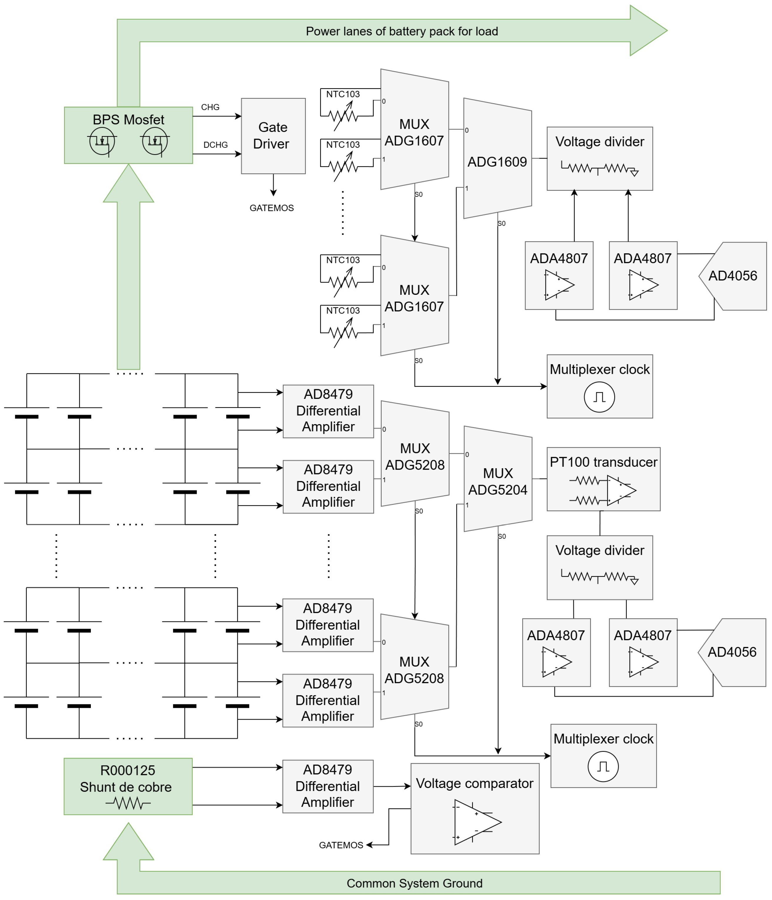
To overcome these challenges, this work proposes a specific BMS architecture (Figure 1), designed to comprehensively detect and manage faults in the cells, the system itself, and the connected loads. The study delves into cell modeling using equivalent circuits validated against empirical data, and concludes with simulations evaluating the efficiency of active balancing and protection mechanisms to ensure safety in high-demand applications.

2. Materials and Methods

The present work presents the development and modeling of a high-efficiency BMS focused on critical light-duty electromobility and energy storage applications in harsh environments (Figure S1). In this context, a harsh and critical application environment refers to operational conditions where the system must face extreme temperature variations, high humidity, mechanical vibrations, electrical shocks, intensive charge and discharge cycles, exposure to electromagnetic interference, and potential risks of internal or external failures that could compromise the safety, performance, or durability of the cells. These conditions require the BMS not only to ensure a safe operation of each cell but also to maintain energy efficiency and protect the system’s critical components under adverse operating scenarios.
The proposed BMS is based on active balancing techniques and additional safety with redundancy in acquisition and sensing, to manage faults in LiFePO4 cells as well as in high-priority loads. The materials, modeling and simulation methods, and tools used for BMS modeling, implementation, and validation are described below. It is important to clarify that, for this specific case, the critical application scope encompasses situations where the system is subjected to severe electrical stress during charge or discharge cycles. Consequently, the constant supervision of current, voltage, and temperature is prioritized, as these variables provide a comprehensive view of the system’s state under adverse electrical conditions.

2.1. BMS Functional Requirements in the Event of Events

To ensure the proper sizing of the BMS, it is imperative to consider the critical events and fault scenarios that modern power storage systems are required to withstand [6]. Based on this premise, the objective is to construct a simulation model capable of meeting these technical requirements while maintaining an optimal trade-off between model complexity and computational efficiency. Furthermore, it should be noted that the majority of the events outlined below are supported by current international standards outlined in Table 1; these regulations define the expected system response for large-scale storage applications, thereby establishing a solid baseline for safe operation [7].
In alignment with these requirements, specific architectural decisions were implemented to bridge the gap between regulatory standards and the proposed simulation model:
  • Short-circuit protection: To comply with total cutoff requirements, a high-side MOSFET driver stage was implemented, controlled by high-speed comparators. These operate independently of any data acquisition instance to ensure that the current to the load or charger reaches zero immediately during a fault.
  • Voltage monitoring: Control and protection stages are conditioned through multiple analog multiplexer (MUX) stages before reaching the Analog-to-Digital Converter (ADC), ensuring signal integrity.
  • Cell Balancing: Individual cell balancing and operational range management are handled by power controllers organized in 6-cell battery packs.
  • Thermal Management: This is managed through conditioning stages using low-internal-resistance MUXs and a dedicated conditioning circuit for voltage-signal outputs.

2.2. Electrochemical Model of Cells

The primary methods for cell modeling are categorized into four main techniques: empirical, electrochemical, data-driven, and equivalent circuit models (ECMs). For this specific work, we selected the General Non-Linear (GNL) equivalent circuit model [8], developed by Saxena, Kulkarni, and Agrawal. Our LiFePO 4 cells were modeled using an RLC equivalent circuit. This structure, based on RC pairs [9], represents the cell’s Thévenin response and enables the simulation of charging/discharging dynamics as well as capacity fade over time. The GNL model was specifically chosen for this work due to several advantages:
  • Ease of Use: It simplifies the complex chemical behavior.
  • SOC Prioritization: It uses the State-of-Charge (SOC) as the primary reference point for both steady-state and dynamic analysis.
  • Low Computational Burden: It requires minimal computational power for execution.
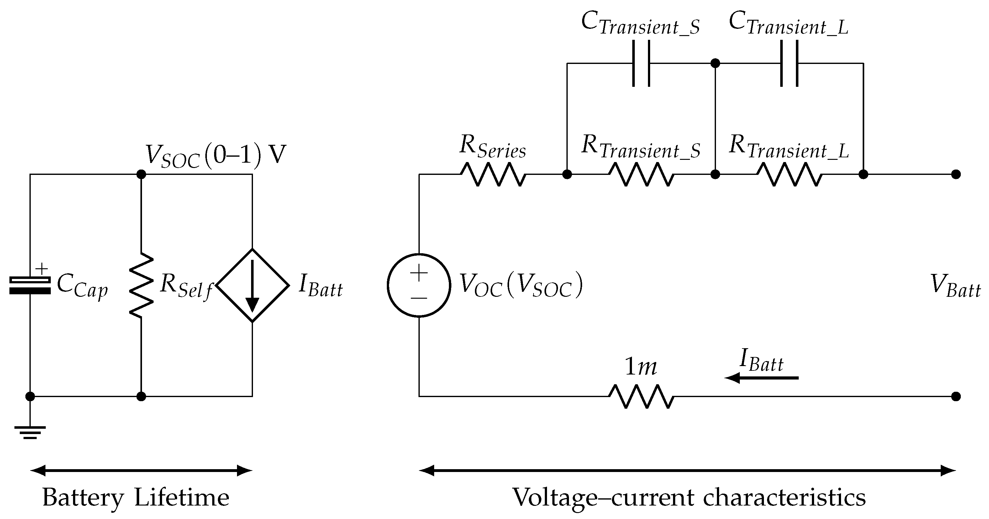
It must be noted that, like most RC models, validation against empirical data is necessary. Nevertheless, the model’s ease of integration into SPICE tools as an equivalent circuit [Figure 2], coupled with the ability to incorporate IC macromodels from various manufacturers, significantly streamlined the implementation of our system. For practical system purposes, chemical-level effects are neglected to simplify the analysis. A key challenge, however, lies in the complexity of the parameterization required to accurately identify the process, given that the cell’s behavior is entirely dependent on the RLC components defined in the model [8].

3. Main Features

  • C. Cap: Capacitance is proportional to the Ah (ampere-hours) of the cell.
  • R. Self: Represents a high-value resistance that is part of the natural self-discharge circuit that the cell has due to its electrochemical properties.
  • I. Batt: Current source dependent on the value obtained from the shunt resistance.
  • V OC (V SOC): Source dependent on V SOC ; the resulting equation gives the cell’s charge and discharge curve.
  • Open Circuit Voltage (OCV): Establishes the non-linear relationship between the state of charge (SOC) and the cell voltage.

3.1. Equations

Taking into account the modeling guidelines of Kulkarni and Agrawal, we have the following equations for each essential part of the GNL circuit [10].
V O C ( S O C ) = 1.031 e 35 S O C + 3.685 + 0.2156 S O C 0.1178 S O C 2 + 0.3201 S O C 3
R S e r i e s ( S O C ) = 0.1562 e 24.37 S O C + 0.07446
R T r a n s i e n t _ S ( S O C ) = 0.3208 e 29.14 S O C + 0.04669
C T r a n s i e n t _ S ( S O C ) = 752.9 e 13.51 S O C + 703.6
R T r a n s i e n t _ L ( S O C ) = 6.6038 e 155.2 S O C + 0.04984
C T r a n s i e n t _ L ( S O C ) = 6056 e 27.12 S O C + 4475

3.2. Model Parameters

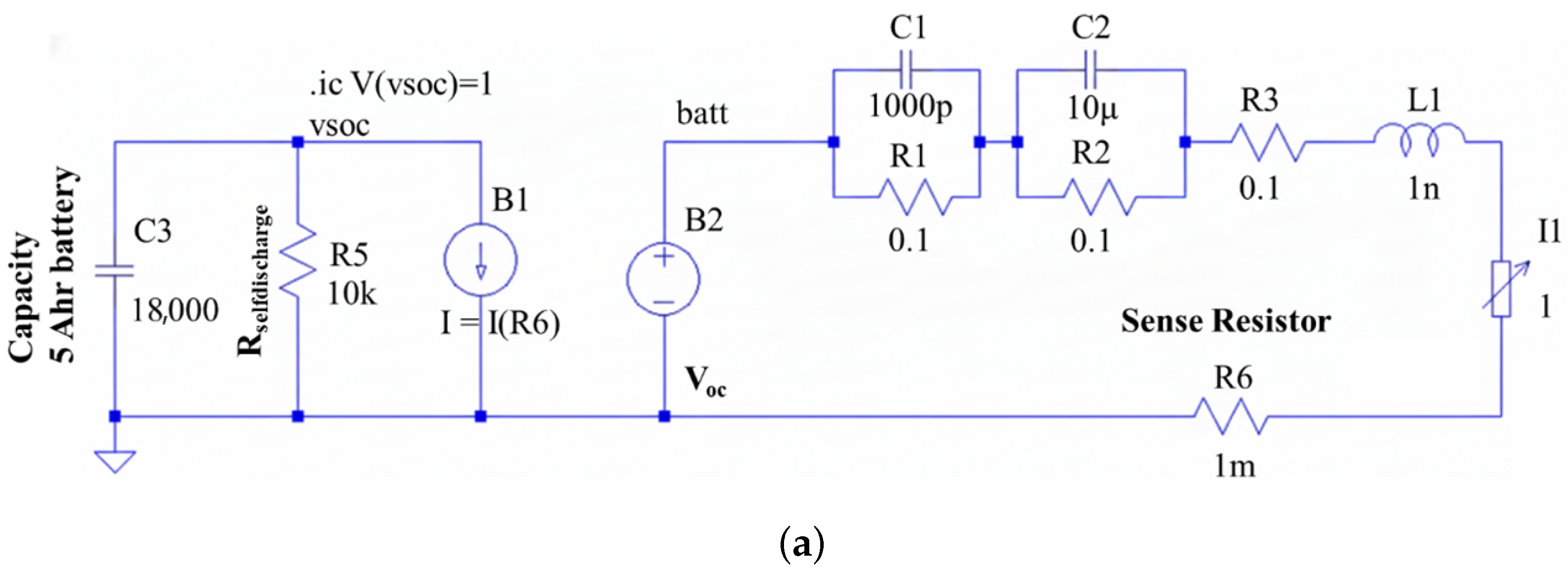
The values of R and C were adjusted based on experimental data obtained through 140 low-current charge–discharge tests, using a set of 3.6 V LiFePO 4 cells with a capacity of 5000 mAh. Consequently, the equivalent circuit model described in Figure 3 is obtained.

3.3. BMS System Design and Active Balancing Techniques

The BMS design is grounded in an active balancing approach to ensure SOC equalization among cells, a critical factor for enhancing battery efficiency and lifespan. This active balancing is implemented using a bidirectional DC–DC topology.
The preference for active over passive balancing is driven by its bidirectional capability to transfer charge between cells, thereby optimizing the SOC in every cycle and preserving the State of Health (SOH) over the long term. Furthermore, active balancing offers significantly superior energy efficiency and thermal management for stacked cell systems compared to dissipative passive methods [11].
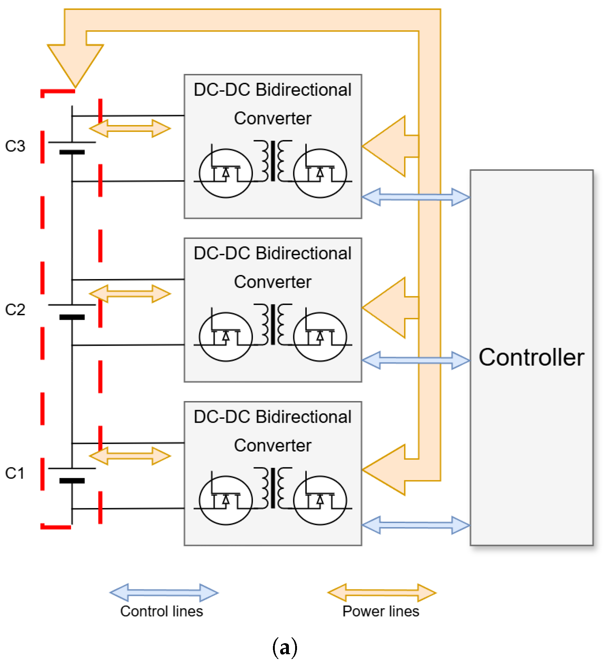
Based on previous research on active balancing methods for electromobility, the CTPTC (Capacitor-Based, Transformer-Based, Port-To-Cell) topology was selected [12], whose control and power characteristics are described in Figure 4a.
This choice is justified by characteristics ideal for high-performance electromobility. According to the available literature (summarized in Table 1), this topology effectively synergizes the strengths of capacitor-based (CTP) and transformer-based (PTC) approaches, yielding two critical advantages for dynamic applications: high speed and flexible energy routing [13].
Although the CTPTC topology entails high control complexity and increased physical volume and cost—trade-offs deemed acceptable for critical, high-performance applications—its combined efficiency and high-speed capabilities render it superior to other alternatives for achieving robust and dynamic balancing within the battery pack.
With these considerations in mind, and upon evaluating the active balancing controllers available within the LTspice library, the LT8584 and LTC3300-1 were identified as primary candidates.
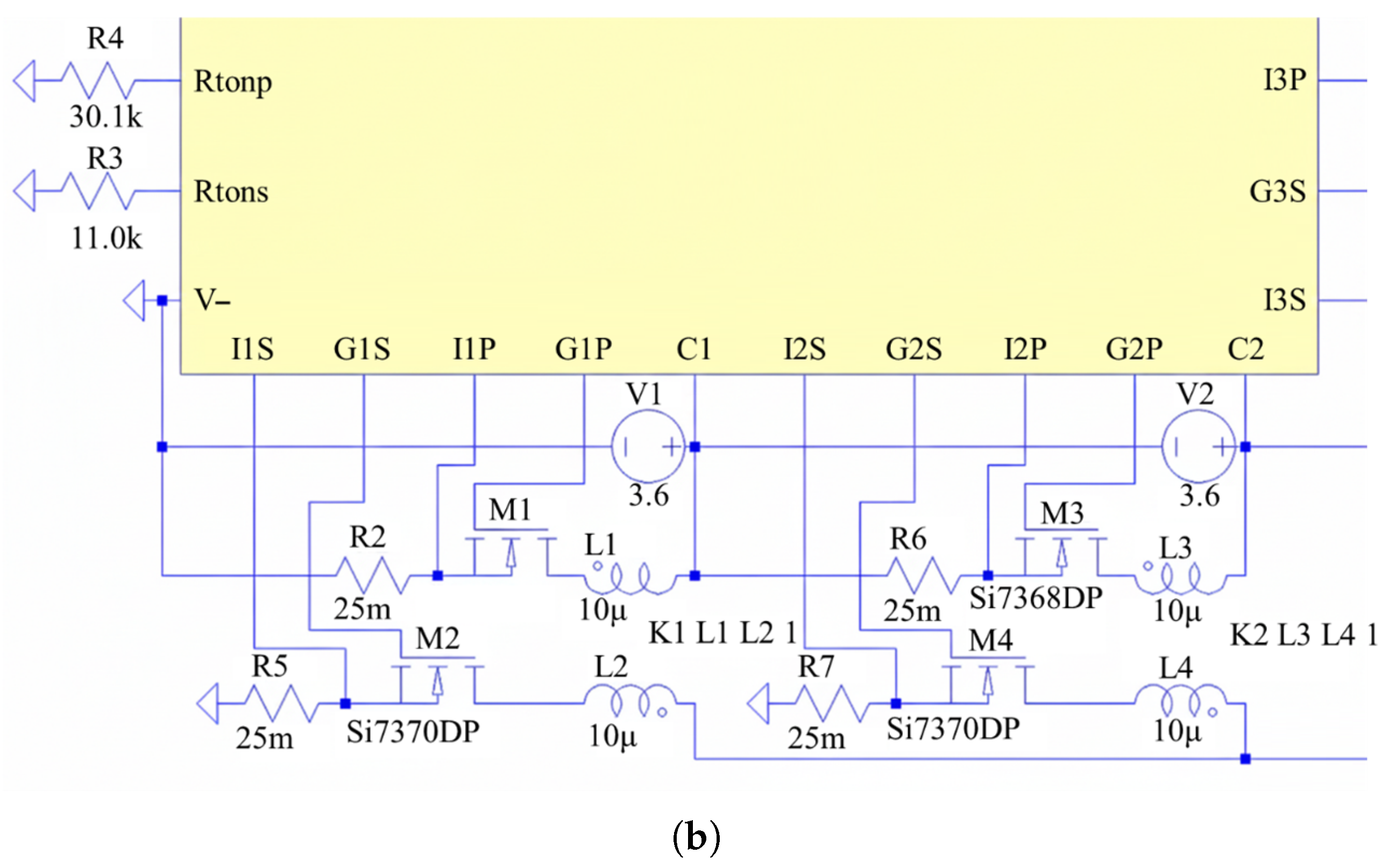
Although prior work utilizing the LT8584 [14] and LTC3300-1 [15] exists and provides a basis for initial development, the LTC3300-1 was selected for this implementation. This decision is justified by its superior stackability for high-cell-count systems, its versatile operating modes, and the higher efficiency specified by the manufacturer. The general application model is presented in Figure 4b.

4. Design and Construction

4.1. Overview of the Acquisition Stage

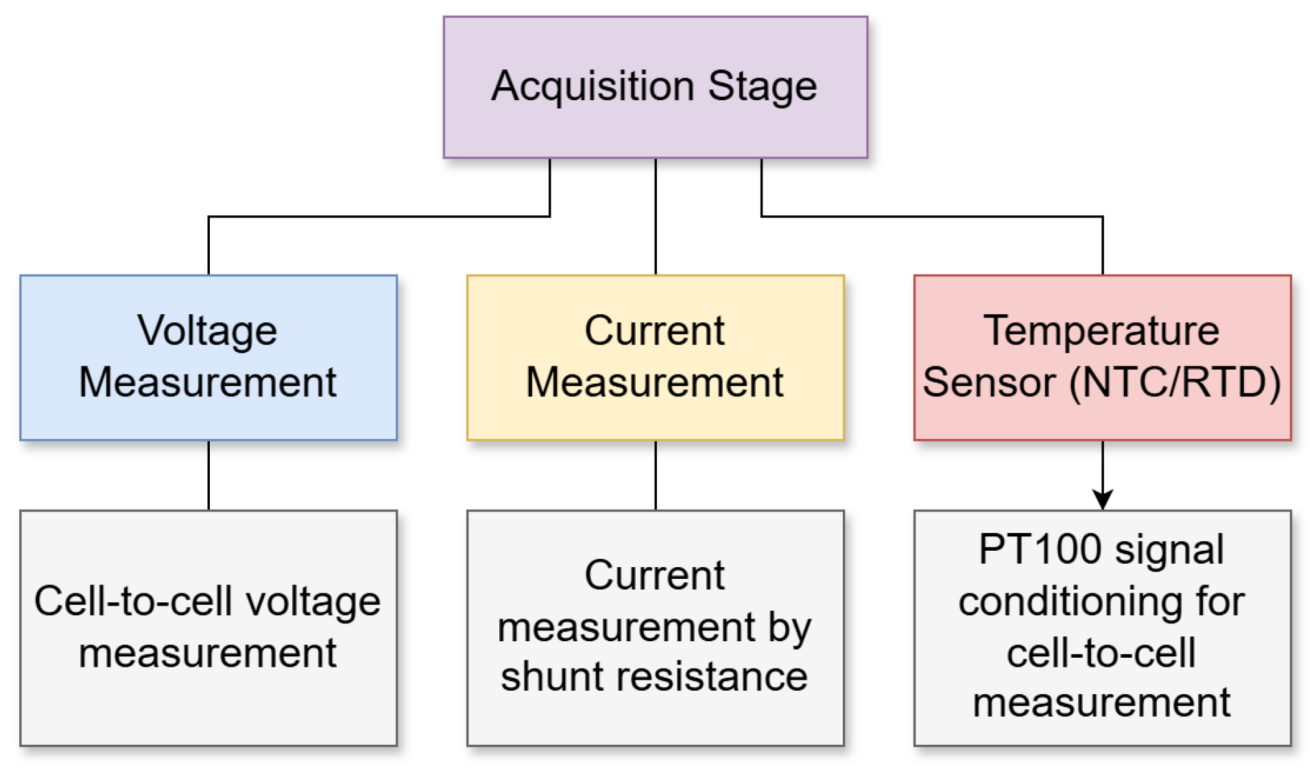
The design of the temperature, voltage, and current acquisition stage is based on measuring each group of series-balanced cells associated with the LTC3300-1, as well as reading NTC/RTD sensors distributed throughout the battery pack—a topology widely employed in most industrial standards to mitigate overheating issues [3].
This stage is overlaid on primary passive-balancing monitors and controllers, such as the LTC6804, which serve as the main monitoring system, while the proposed acquisition system operates as a redundant safety monitor [4]. This topology is presented in greater detail in Figure 5 and Figure S2.
To address the physical implementation of this simulated architecture, non-ideal hardware effects have been considered. Although the current validation relies on simulation, the design incorporates high-resolution analog-to-digital converters (ADCs) capable of performing digital filtering to compensate for the limitations of analog signal conditioning circuits. Given that the signals are predominantly DC, measurement errors and switching non-linearities can be effectively mitigated through these digital strategies. Furthermore, data reliability in a real-world environment will be ensured by adhering to IPC standards for PCB design and employing metallic shielding to neutralize noise caused by induction and electromagnetic radiation.

4.2. Cell Stacking and Active Balancing Stage

In the power stage, the stacked cell system was implemented based on lithium equivalent circuit models. To reduce the simulation’s computational burden, the model was simplified by retaining only the dependent voltage and current sources for each cell, as well as their internal series resistance. Specifically, a series array of 24 GNL equivalent circuit cells was configured for this implementation (Figure S3a).
An LTC3300-1 [16] active balancing unit was integrated in parallel with each 6-cell module. The architecture consists of three balancers configured in series, while the fourth unit is configured as the top-of-stack device (Figure S3b).
Finally, this power subsystem is fully interconnected with the control, protection, and data acquisition stages.
Regarding the scalability of this configuration, it should be noted that the primary challenges lie in the dielectric breakdown limits of the top-of-stack controller and the high-side power components. Although the system employs differential measurement (utilizing the AD8479) [17], ensuring a high Common Mode Rejection Ratio (CMRR) is essential to prevent electrical breakdown before the signals are referenced to ground.

4.3. Cell Voltage Front-End and Primary Multiplexing

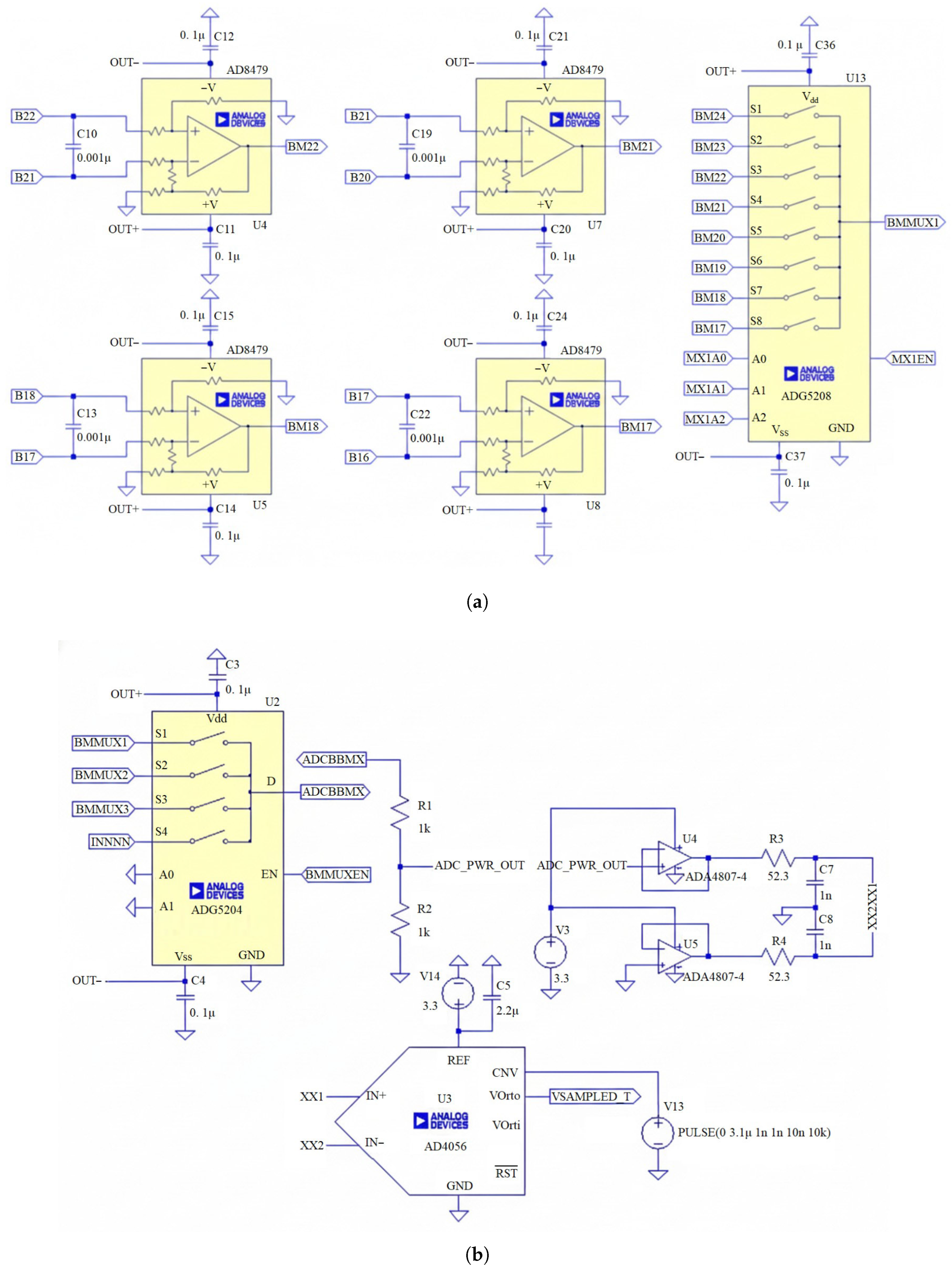
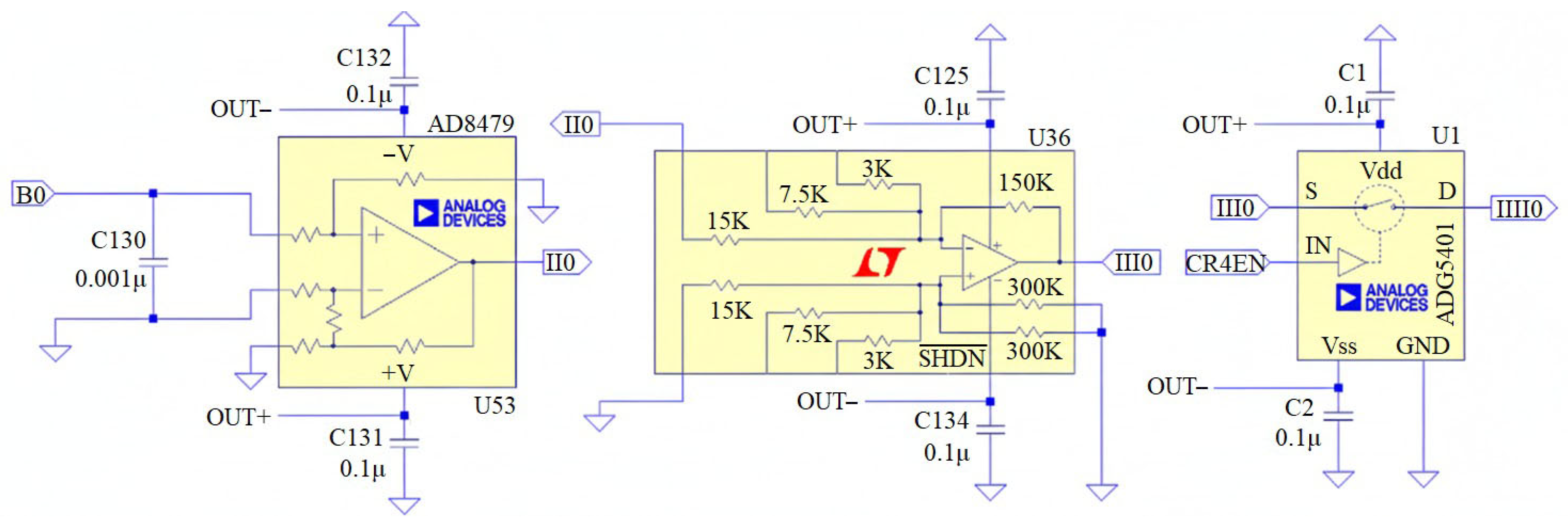
The cell-voltage acquisition system is implemented with a current shunt on the low side of the pack and a differential front-end for each group of cells. For each cell terminal pair, an AD8479 instrumentation amplifier [17] configured with unity gain and very high CMRR (up to 600 V) is used, allowing each cell voltage to be measured independently even in the presence of large common-mode voltages. The outputs of these front-ends (BM17…BM24) are applied to an ADG5208 analog multiplexer [18], which sequentially selects each cell-measurement channel (Figure 6a). Thanks to this architecture, it is possible to compare the condition of the series cell strings and obtain a clear reference of the entire pack voltage, while keeping the MUX stage isolated and protected from transients on the battery bus.

4.4. Secondary Multiplexing, Level Adaptation, and High-Accuracy ADC

In the pack voltage acquisition system, the front-end stage described in the previous section protects the ADG5208/ADG5204 industrial multiplexers [19] due to its high CMRR. The signal selected by the MUX is applied to a resistive voltage divider to adapt the input range to the limits allowed by the ADC (Figure 6b).
Subsequently, the signal passes through a buffer stage composed of the ADA4807 [20], which acts as an ADC driver to deliver the signal to the AD4056 converter [21], serving as a high-speed, high-resolution digitizer. It should be noted that, since the simulation platform used does not permit verification of the AD4056 SPI interface, the analysis focuses on the analog signal integrity.
The combined use of a high-CMRR front-end and low-leakage industrial multiplexers improves noise immunity and prevents the reliability of measurements from each individual cell being compromised.

4.5. Symmetric Supply for the Analog Front-Ends

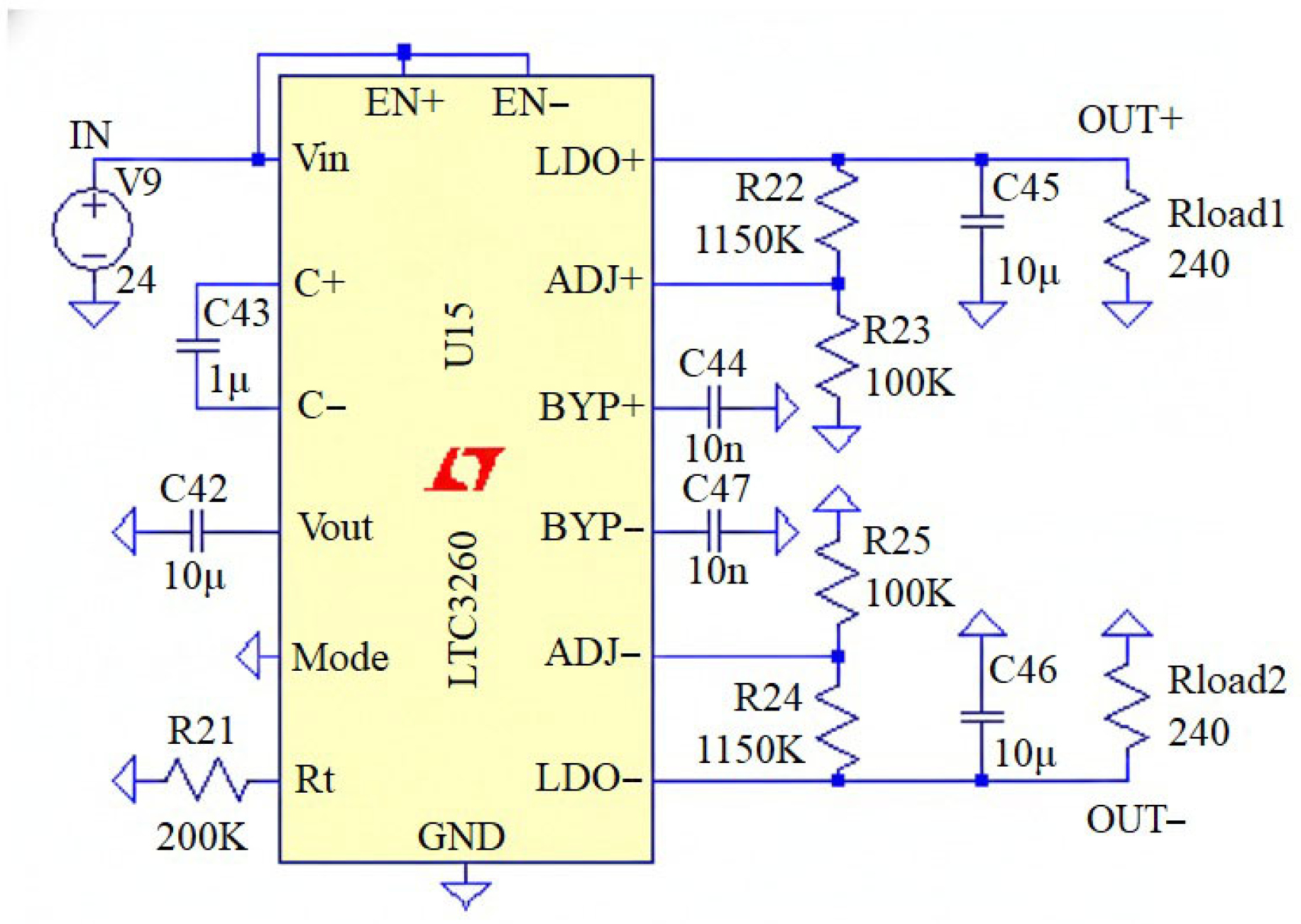
The instrumentation amplifiers and signal-conditioning stages are powered from a symmetric supply (Figure 7). generated by the LTC3260 [22]. This circuit produces positive and negative rails from the input bus, allowing the AD8479 and LT1997-1 [23] stages to operate with sufficient headroom for bipolar signals and improving the margin in the presence of line transients. Proper decoupling using 10 µF and 0.1 µF capacitors on each rail minimizes noise injection into the measurements.

4.6. Battery Pack Current Sensing

The response to short-circuit, overcharge, over-discharge, and load disconnection events is managed primarily through continuous current monitoring. Consequently, it is imperative to account for potential failure scenarios throughout the design, sizing, and commissioning phases to ensure the effectiveness and robustness of the protection schemes [6]. For the current-sensing stage implementation, an AD8479 is again utilized as a differential front-end, connected to a shunt resistor of approximately 1 m Ω in series with the battery pack. The shunt value is selected based on the calculation of the maximum allowable power dissipation for the sensing elements, ensuring an optimal trade-off between voltage drop and self-heating (Figure 8). The differential signal, amplified by the AD8479, is subsequently applied to an LT1997-1 amplifier configured with a gain of 10 to boost small current variations. Finally, the output of this stage is routed to a voltage divider and proceeds to the ADC drivers, following the same signal processing chain previously employed: level adaptation (LT1997-2), ADC driving via the ADA4807, and final conversion in the AD4056 ADC.

4.7. Temperature Multiplexing with 2-Wire PT100 Sensors

The temperature acquisition system relies on analog multiplexers to switch between multiple sensors distributed across the pack. In the configuration shown, 2-wire PT100 sensors are used, connected in pairs to one ADG1607 [24] for each group of 8 sensors. The different RTD branches and 80 k Ω resistors define the excitation currents and measurement points (Figure S4). The outputs of the ADG1607 devices are grouped and fed into a second MUX, the ADG1609 [25], which selects the active temperature channel toward the analog conditioning stage. Channel switching is controlled by a microcontroller with a period shorter than 1 ms, making it possible to scan the thermal distribution of the pack quickly.

4.8. DAC Stage and Conditioning for Temperature Measurement

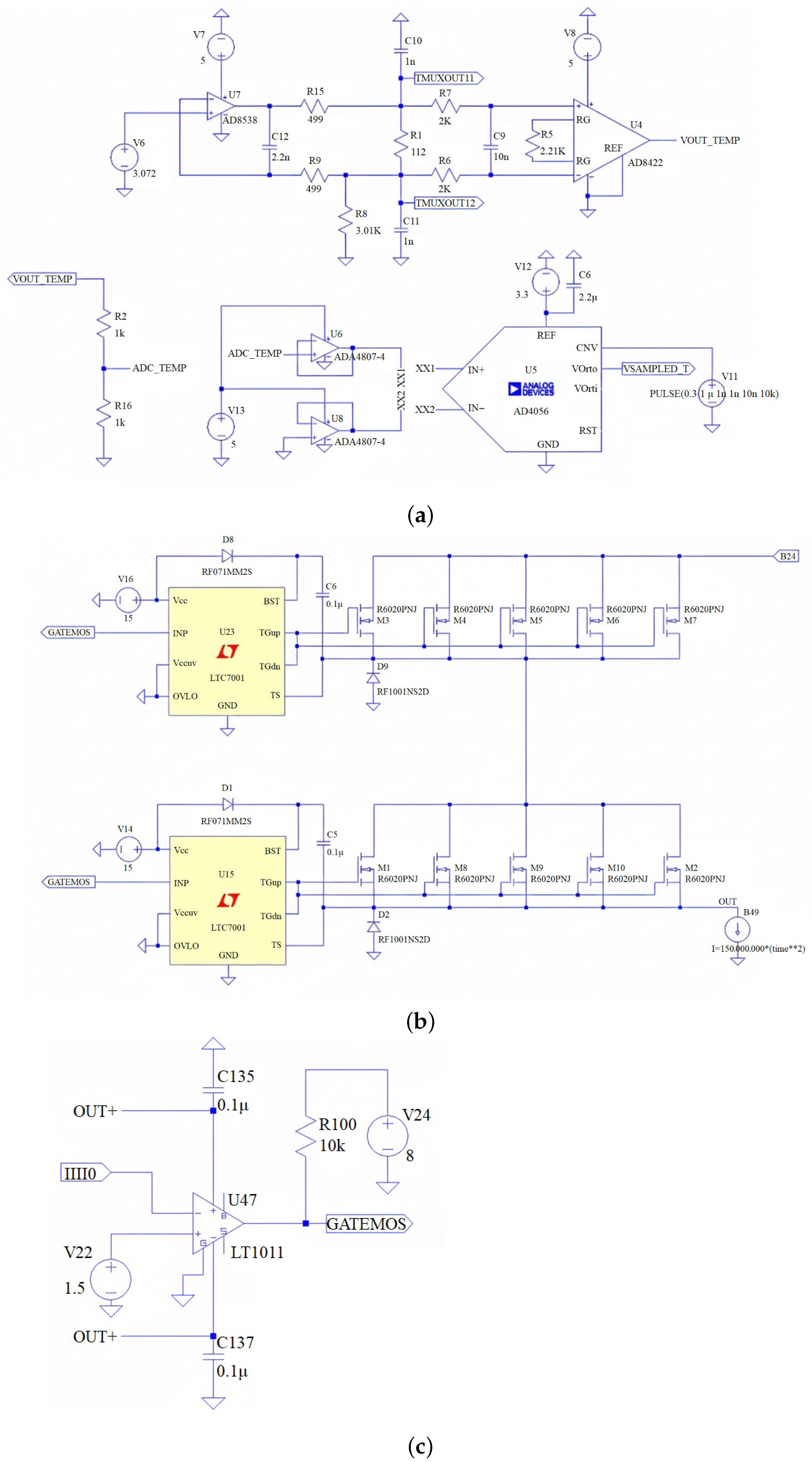
The stage associated with the DAC and precise temperature measurement is analogous to the one used in the current and voltage system, but it incorporates an additional transducer to semi-linearize the relationship between output voltage and temperature (Figure 9a).
Precision reference LTC6655 (3.3 V and 5 V) and LT1086 regulators are used to generate the supply voltages for the measurement circuitry. A resistor network (R63–R64) divides a 4.096 V reference to obtain the VCC_4.096_DIV level, which is conditioned by an AD8538 amplifier [26].
Subsequently, an AD8422 [27] instrumentation amplifier sets the gain and enables adjusting the overall response so that the output voltage is almost linear with the temperature measured by the sensors connected to the multiplexer.
The conditioned signal is finally fed to the AD4056 ADC, sharing the same ADA4807 driver front-end to ensure consistent conversion with the other quantities measured in the system.

4.9. High-Side Protection Stage with MOSFETs

The power-protection stage is based on an array of R6020PNJ N-channel MOSFETs connected on the high side of the battery pack. A high-side driver LTC7001 [28] is used to raise the gate voltage above the bus potential, allowing the MOSFETs to switch properly even with up to 24 cells in series (maximum voltage ≈ 100.8 V) (Figure 9b).
To improve safety and enable bidirectional conduction—from the charger to the cells and from the cells to the load—the MOSFETs are arranged in a back-to-back configuration. In this way, current is limited under overload, short-circuit or system-fault conditions, while the effective on-resistance during normal operation is kept low.

4.10. Voltage Comparator as a Protection Trigger for MOSFETs

Regarding the triggering of the high-side MOSFET electronic protection, two primary approaches exist for implementing an electronic fuse: utilizing a digital control loop via a microcontroller ADC, or employing dedicated hardware-based control. The latter provides a superior response speed and reliability for protection triggering.
Given that this application requires an enhanced safety level, the hardware approach was selected. Specifically, the LT1011 [29] was chosen to function as a high-speed comparator connected to the low-side current shunt.
This configuration (Figure 9c) ensures robustness against fast transient events. Furthermore, this topology is replicable for monitoring temperature, voltage, or any parameter requiring minimal actuation latency.

4.11. Microcontroller Model in SPICE

For this specific case, SPICE directives (Figure S5) were employed alongside behavioral sources and a subcircuit designated as ‘MCU’ to emulate microcontroller operation [30]. This model generates a 16 kHz PWM signal on its high-speed output and manages five control lines for the multiplexers. Additionally, this configuration allows for the integration of directives to implement comparison-based control, signal management, or complex mathematical functions.
However, the use of these logic-based directives was minimized in favor of hardware-based responses. The objective of this strategy is to accurately simulate the propagation delays inherent to the control, protection, and acquisition stages.

5. Results

This chapter presents and analyzes the results obtained from the validation tests performed on the designed Battery Management System (BMS) model. The main objective of these trials is to verify compliance with design parameters and system stability under both nominal and fault conditions.
The presentation of results follows a modular structure: it begins with the characterization of the Lithium-Ion cell model powering the system; subsequently, the performance of the data acquisition subsystems (voltage and temperature) is evaluated in the frequency domain; finally, the dynamic response of the electronic protection (e-Fuse) and the energy efficiency of the active balancing stage are validated [30].

5.1. Characterization of the Equivalent Circuit Model

Given the specific characteristics of the selected Li-Ion cell model, a simplified implementation was chosen using a controlled voltage source dependent on the charge/discharge current and the State of Charge (SOC).
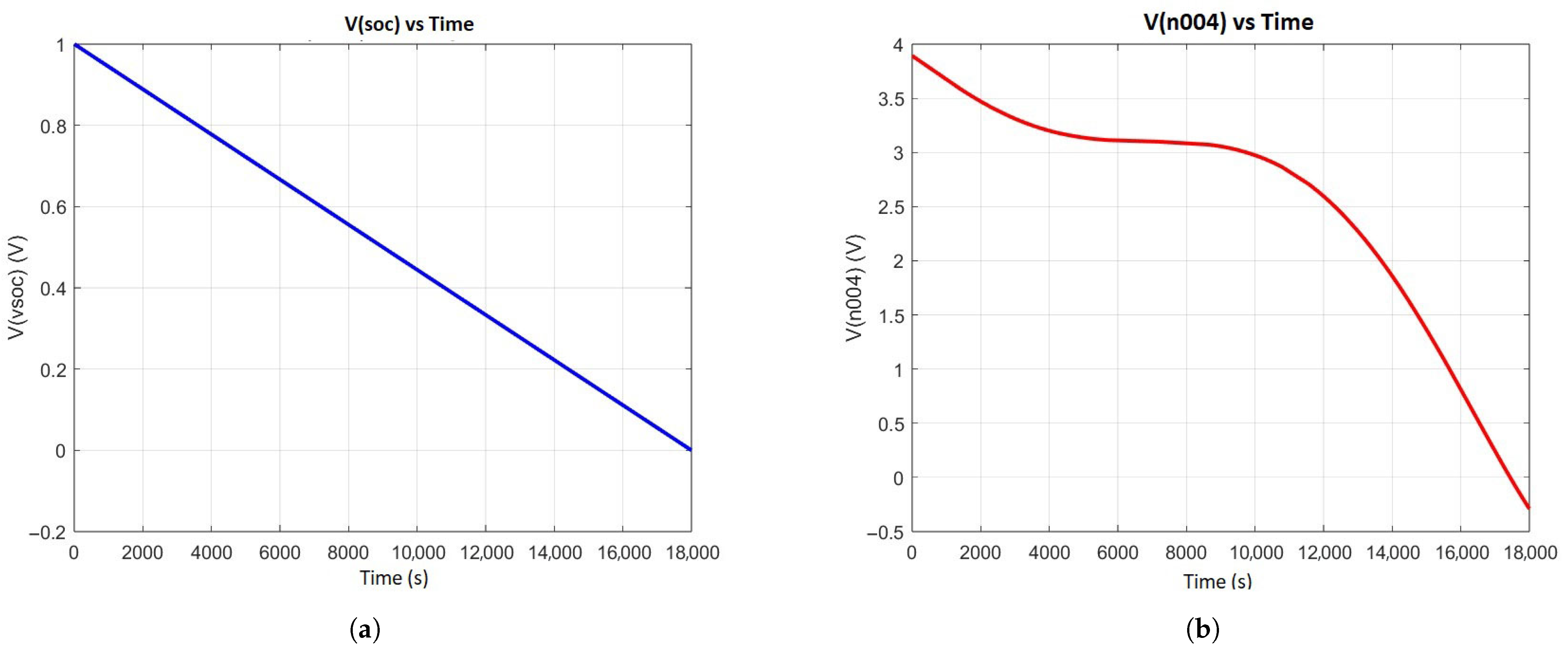
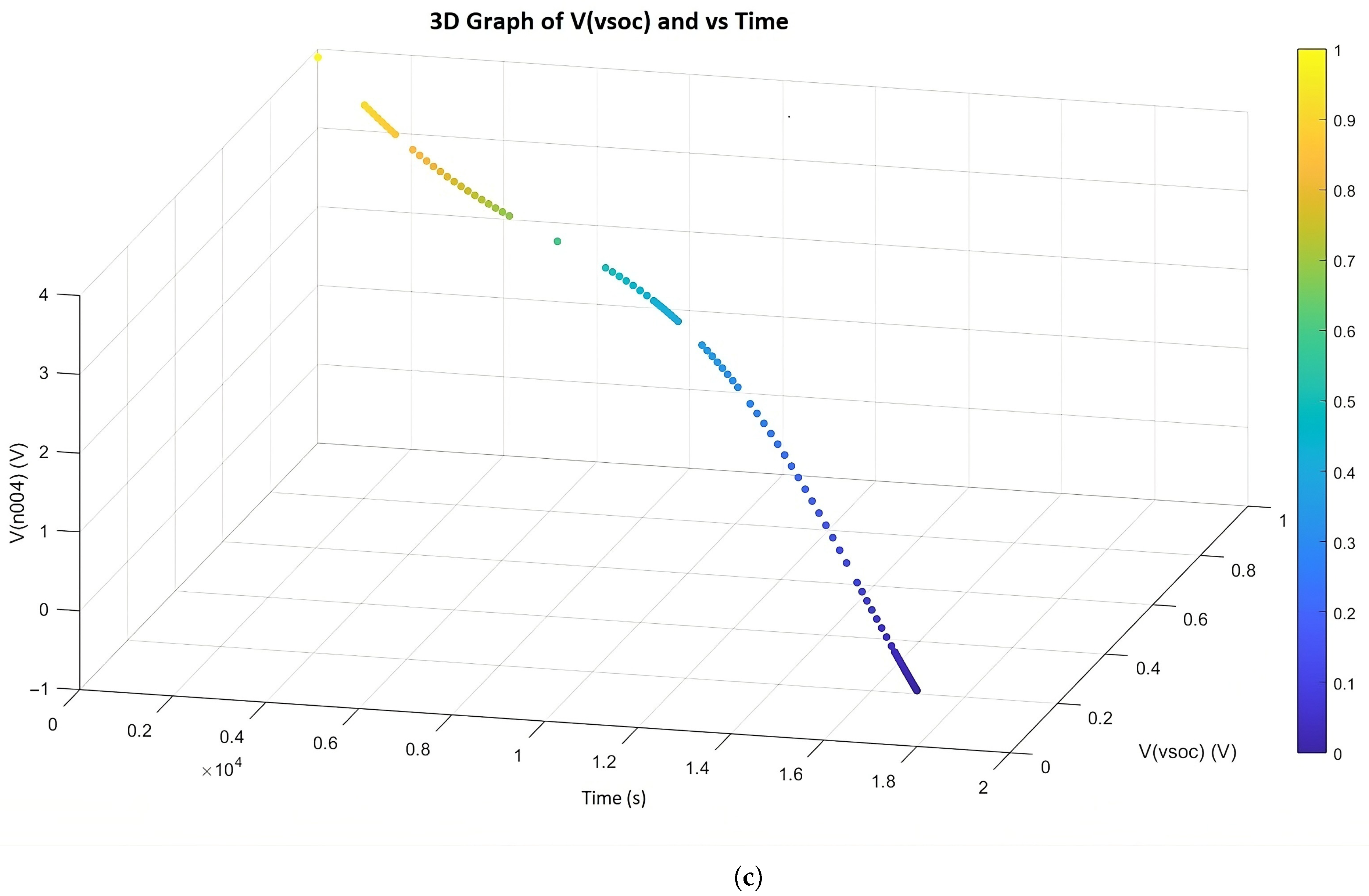
To validate the voltage vs. SOC (VSOC) curve, a constant current discharge of 1000 mA (0.2C) was simulated on a theoretical 5000 mAh cell. As observed in Figure 10a, the resulting linearization curve confirms a useful discharge duration of 5 h, coinciding with the expected theoretical parameters.
Subsequently, the response of the dependent voltage source was adjusted using its characteristic polynomial equation to faithfully represent the Open Circuit Voltage (OCV) at the output terminals (Figure 10b).
The integration of these parameters allowed for the derivation of the complete V–I characteristic curve (Figure 10c), which serves as the baseline for validating the BMS behavior throughout the remaining tests.

5.2. Frequency and Bandwidth Analysis (AC Sweep)

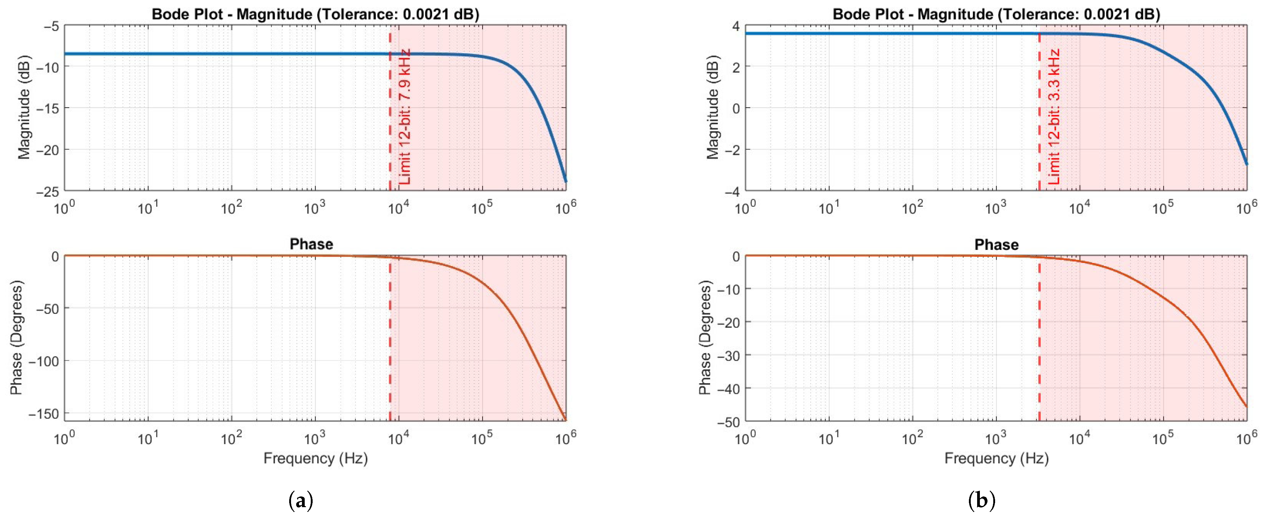
The frequency response of the multiplexing (MUX) and driver stages for signal acquisition was evaluated. The analysis is based on the ADC resolution (12-bit) and the required sampling rate. The 1 LSB (Least Significant Bit) error criterion was used as the tolerance limit to guarantee signal integrity.
E r r o r m a x = V r e f 2 N ,
20 · log 10 1 1 4096 0.0021 dB .
The Bode plot results obtained from the simulation were exported (Figure 11a). The analysis demonstrates that the voltage acquisition stage maintains a flat response within the 1 LSB tolerance up to a frequency of 7.9 kHz. On the other hand, for the temperature acquisition stage, the maximum tolerance is established at 3.3 kHz. This confirms that the bandwidth of the ADG5204 MUX is sufficient to capture battery dynamics without introducing significant attenuation (Figure 11b).

5.3. Precision in MUX and Temperature Conditioning Stages

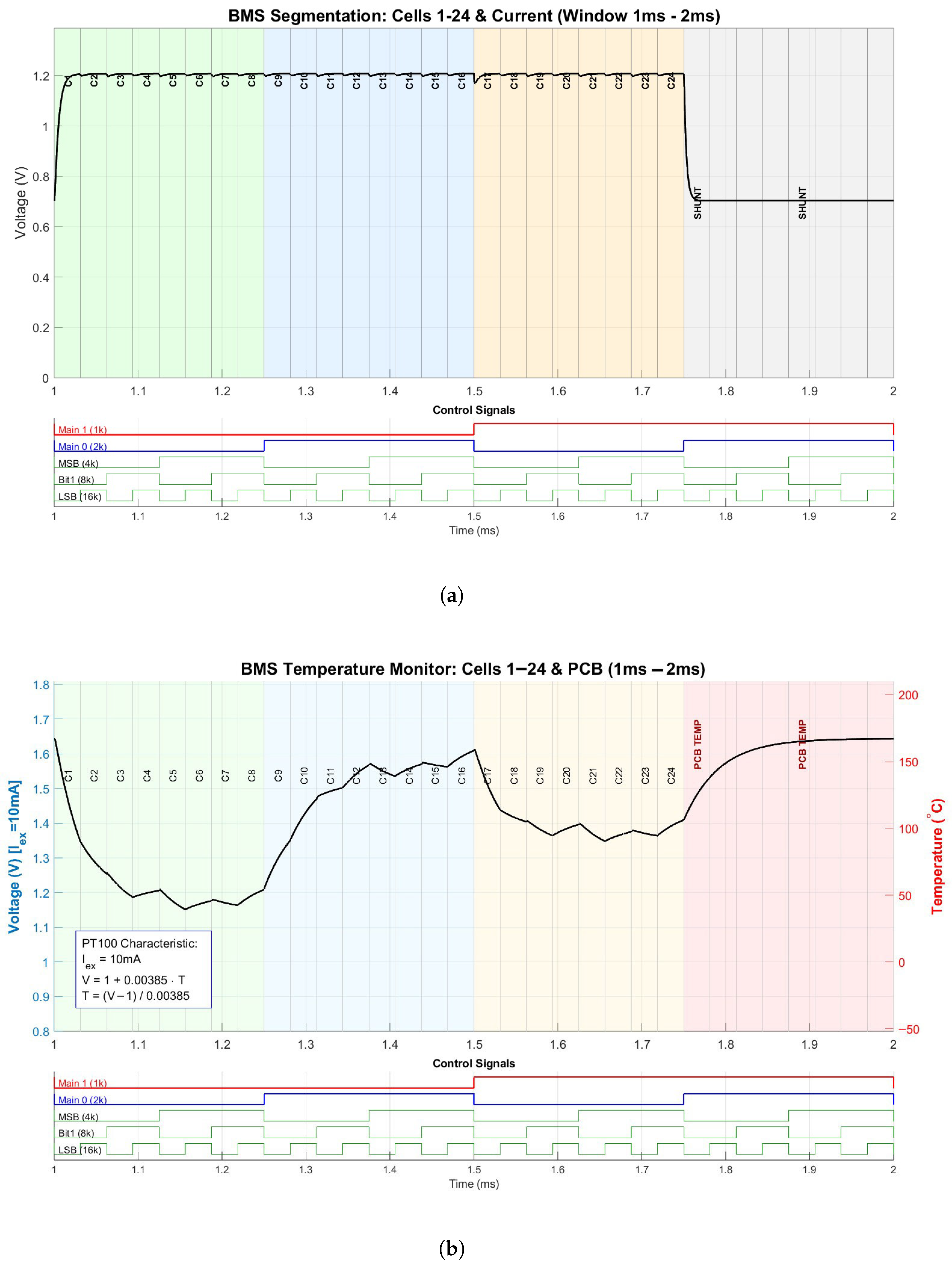
As detailed in the design, the channel selection of the MUXs responds to a switching clock configured at 16 kHz. Channel switching in analog multiplexers generates a glitching effect (switching transients), which must be attenuated via additional output capacitance. The advantage of using MUXs with optimized input impedances ( 160 Ω in the ADG5208 and 160 Ω in the ADG5204) is that they mitigate the effect of interfering signals (crosstalk) on disabled channels. The image below visualizes the channel transition, the logic configuration, and the resulting waveform conditioned for the ADC (Figure 6). Regarding the individual temperature reading obtained from the MUXs (at the fundamental frequency of 16 kHz), this signal originates from the excitation and conditioning stage for the PT100 sensor. The system response as a function of the selected channel, measured temperature, and control signal is shown below (Figure 12).

5.4. Protection Tests: Electronic Fuse (e-Fuse)

A current transient with quadratic behavior was simulated using the coupled cell models and their characteristic discharge curve. The discharge is visualized in terms of voltage vs. current, total power dissipated, and its temporal evolution (Figure S6a).
Additionally, the readings taken at the output of the multiplexer stage are presented along with their respective control signals, confirming the detection of the event [31] (Figure S6b).

Dynamic Connection and Disconnection Characterization

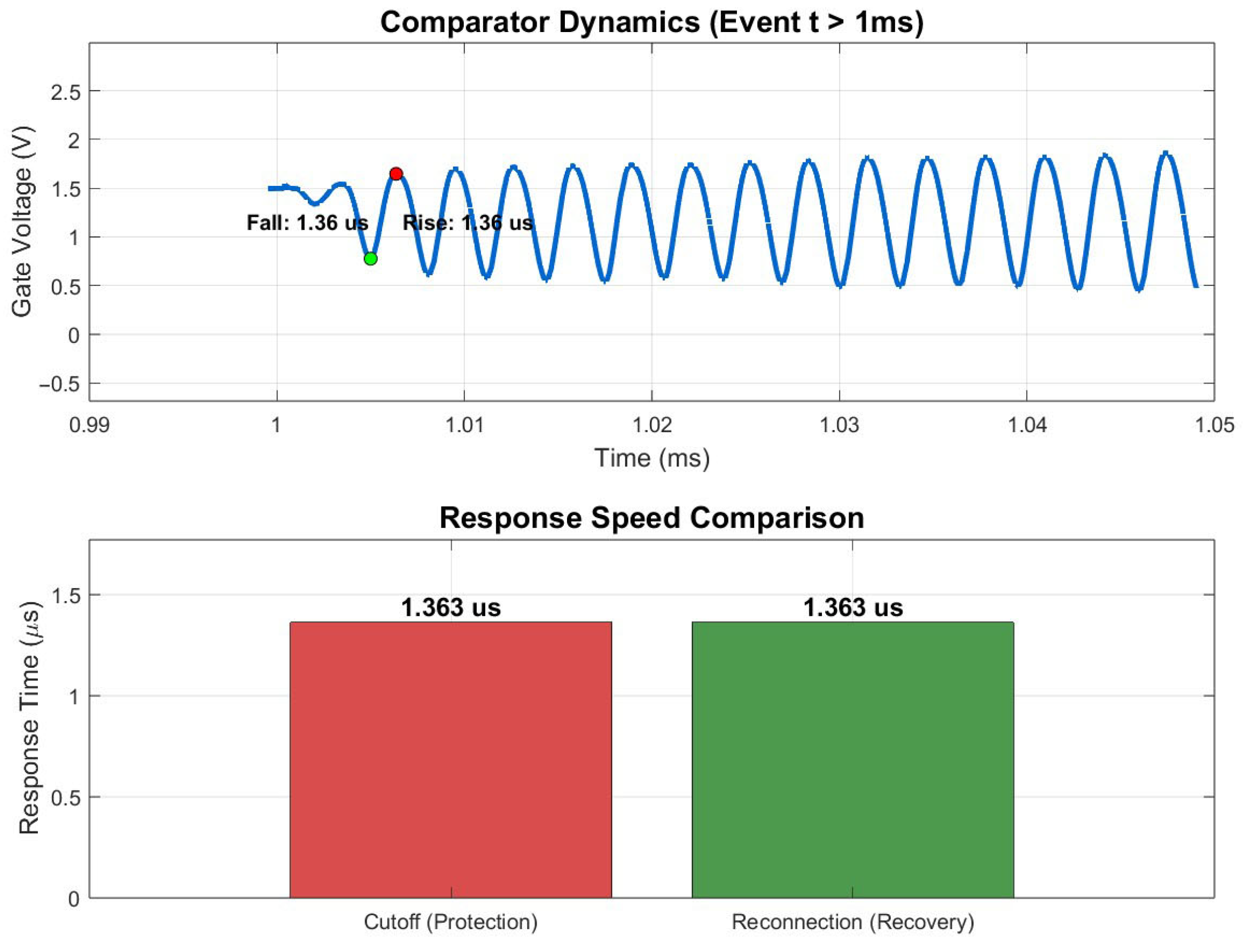
To measure the system’s response times, the comparator was connected to the shunt resistor to control the MOSFET gates without enabling the latching mechanism. This configuration allows for the evaluation of the dynamic response under a sustained fault condition, forcing connection and disconnection cycles (controlled oscillation). Figure 13 shows the response curve under this condition without error memory. This test validates the reaction speed of the drivers and MOSFETs, demonstrating the delay times (rise and fall times) necessary to ensure safety disconnection in the event of an overcurrent.

5.5. Active Balancing System Efficiency (LTC3300-1)

Finally, the performance of the conversion system based on the LTC3300-1 controller was evaluated. Characteristic curve tests were performed on the voltage in both charge and discharge modes.
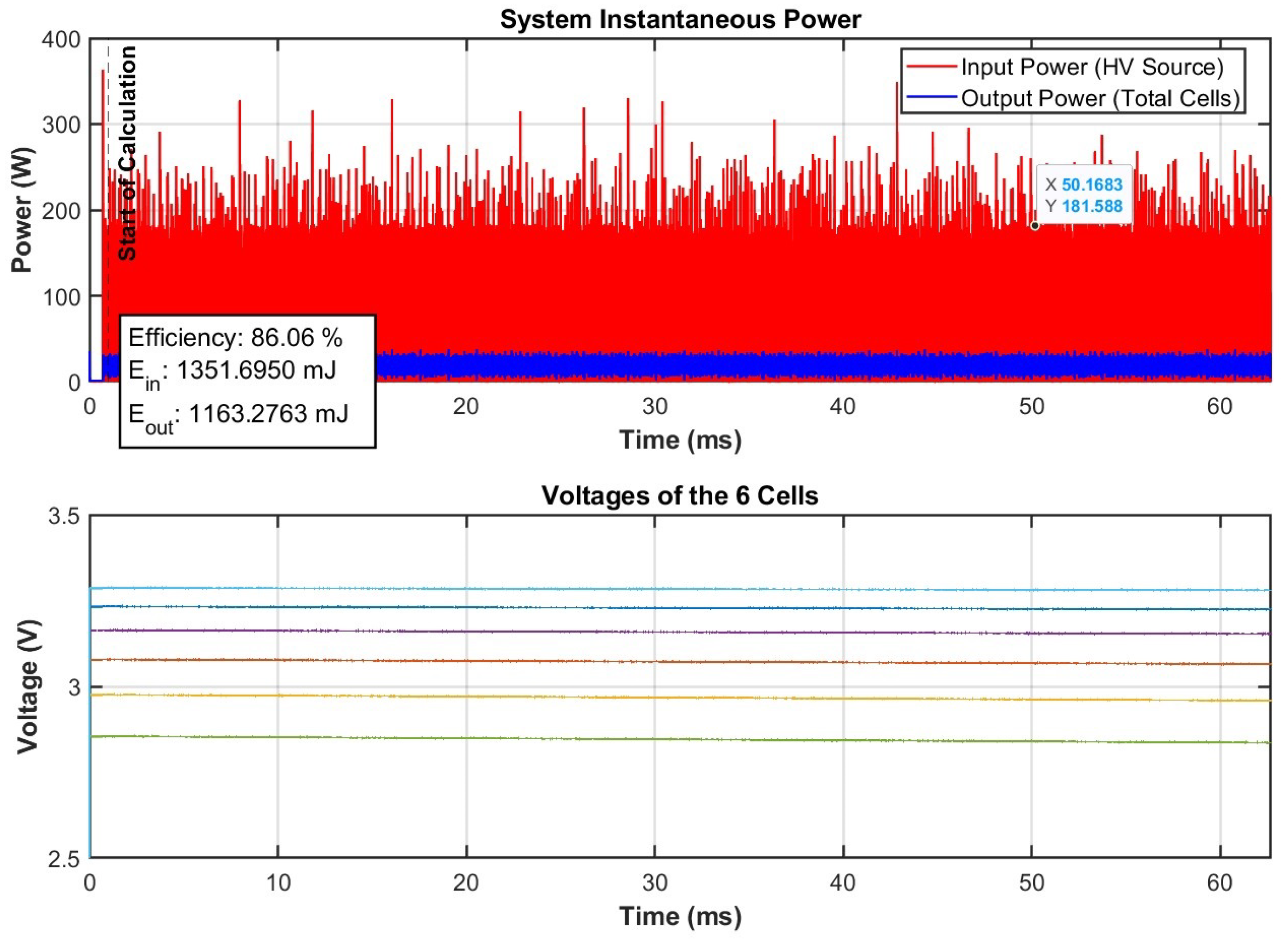
To simplify the computational load without sacrificing the validity of the test, 6 reference cells were attached to one of the LTC3300-1 controllers and configured with different States of Charge (SOCs) to force energy transfer. The objective was to measure (Figure 14) the overall efficiency of the system. The results indicate an efficiency of approximately 86%, a value considered sustainable and suitable for active balancing systems of this degree of complexity.

6. Conclusions

In conclusion, the development of this project demonstrated the technical feasibility of simulating the critical aspects of a modern BMS, successfully integrating the requirements for data acquisition, protection, and lithium cell balancing.
It was determined that the cutoff response capability with respect to external and internal stimuli is the determining factor in ensuring operational stability. Through the analysis performed, it was validated that the proposed topologies and sizing meet necessary safety standards, highlighting that an active balancing strategy not only improves immediate safety but is also fundamental for prolonging the long-term lifespan of the battery bank.
Furthermore, this work establishes a technical precedent for the use of LTspice as a robust tool in BMS modeling. It is concluded that simulation should not be viewed solely as an academic stage, but as a critical engineering phase that allows for the prediction of complex thermal and electrical behaviors. This significantly reduces the costs and risks associated with physical prototyping, enabling more agile design iterations prior to manufacturing.
Finally, while the simulated environment offers a high-fidelity approximation, experimental hardware validation is identified as the logical next step to corroborate the non-linear dynamics of the cells under real-world stress conditions. Nevertheless, the model presented here constitutes a solid and scalable foundation for the development of energy storage systems oriented towards electromobility and high-demand stationary applications.

Supplementary Materials

The following supporting information can be downloaded at: https://www.mdpi.com/article/10.3390/computation14030061/s1, Figures S1–S6: Supplementary Figures cited in the manuscript.

Author Contributions

Conceptualization, M.J.P.-F., M.P.G.-L. and D.E.G.-A.; Methodology, M.J.P.-F. and M.P.G.-L.; Software, M.J.P.-F.; Validation, M.J.P.-F.; Formal analysis, M.J.P.-F. and M.P.G.-L.; Investigation, M.J.P.-F.; Resources, M.P.G.-L.; Data curation, M.J.P.-F.; Writing—original draft preparation, M.J.P.-F.; Writing—review and editing, D.E.G.-A.; Supervision, M.P.G.-L. and D.E.G.-A. All authors have read and agreed to the published version of the manuscript.

Funding

This research received no external funding.

Data Availability Statement

The data supporting the findings of this study are available from the authors upon reasonable request.

Conflicts of Interest

The authors declare no conflict of interest.

References

  1. Mitali, J.; Dhinakaran, S.; Mohamad, A.A. Energy storage systems: A review. Energy Storage Sav. 2022, 1, 166–216. [Google Scholar] [CrossRef]
  2. Zhang, Z.J.; Ramadass, P. Lithium-Ion Battery Systems and Technology. In Batteries for Sustainability: Selected Entries from the Encyclopedia of Sustainability Science and Technology; Brodd, R.J., Ed.; Springer: New York, NY, USA, 2013; pp. 319–357. [Google Scholar] [CrossRef]
  3. Shen, M.; Gao, Q. A review on battery management system from the modeling efforts to its multiapplication and integration. Int. J. Energy Res. 2019, 43, 5042–5075. [Google Scholar] [CrossRef]
  4. Jeevarajan, J.A.; Joshi, T.; Parhizi, M.; Rauhala, T.; Juarez-Robles, D. Battery Hazards for Large Energy Storage Systems. Acs Energy Lett. 2022, 7, 2725–2733. [Google Scholar] [CrossRef]
  5. Chhabria, N.; Jaiprakash, A.; Motwani, K.R.; Srinivasan, R. RLC circuit simulation and Monte Carlo Analysis in MATLAB R2024a. In Proceedings of the 2016 International Conference on Communication and Electronics Systems (ICCES), Coimbatore, India, 21–22 October 2016; pp. 1–6. [Google Scholar] [CrossRef]
  6. Gabbar, H.A.; Othman, A.M.; Abdussami, M.R. Review of Battery Management Systems (BMS) Development and Industrial Standards. Technologies 2021, 9, 28. [Google Scholar] [CrossRef]
  7. Pepo, M.; Fuller, S.; Cseke, T.; Weltsch, Z. Advances in Standardised Battery Testing for Enhanced Safety and Innovation in Electric Vehicles: A Comprehensive Review. Batteries 2025, 11, 157. [Google Scholar] [CrossRef]
  8. Rahmoun, A.; Biechl, H. Modelling of Li-ion batteries using equivalent circuit diagrams. Prz. Elektrotechniczny 2012, 88, 152–156. [Google Scholar]
  9. Kamrueng, C.; Kittiratsatcha, S.; Polmai, S. A Number of RC Pairs Consideration of Electrical Equivalent Circuit Model of Li-ion Battery. In Proceedings of the 2020 6th International Conference on Engineering, Applied Sciences and Technology (ICEAST), Chiang Mai, Thailand, 1–4 July 2020; pp. 1–4. [Google Scholar] [CrossRef]
  10. Kulkarni, M.; Agrawal, V. A Tutorial on Battery Simulation-Matching Power Source to Electronic System. In Proceedings of the 14th IEEE VLSI Design and Test Symposium, Hsin Chu, Taiwan, 26–29 April 2010. [Google Scholar]
  11. Babu, P.S.; Ilango, K. Comparative Analysis of Passive and Active Cell Balancing of Li Ion Batteries. In Proceedings of the 2022 Third International Conference on Intelligent Computing Instrumentation and Control Technologies (ICICICT), Kannur, India, 11–12 August 2022; pp. 711–716. [Google Scholar] [CrossRef]
  12. Kulal, R.; Shambhoji, S.; Patgar, K.; Khatal, P.; Koraddi, S. Analysis of Cell Balancing Techniques for Li-ion Batteries. In Proceedings of the 2024 First International Conference on Software, Systems and Information Technology (SSITCON), Tumkur, India, 18–19 October 2024; pp. 1–7. [Google Scholar] [CrossRef]
  13. Li, H.; Ooi, C.A.; Jia, Z.; Ammar, K.; Ishak, M.K. A review of active cell balancing methods in electric vehicles. Energy Convers. Manag. X 2025, 28, 101244. [Google Scholar] [CrossRef]
  14. Otunubi, L.; Thompson, E.A.; Bender, J.; Jim Eitsert, P. Active LiFePO4 Battery Cell Balancing Based on a Flyback Converter for Battery Storage Application. In 2024 IEEE 12th International Conference on Smart Energy Grid Engineering (SEGE); IEEE: New York, NY, USA, 2024; pp. 241–244. ISSN 2575-2693. [Google Scholar] [CrossRef]
  15. Jin, X.; Li, Y.Y.; Xu, T.; Zhang, Y.H. Active equilibrium control system for li-ion battery base on LTC3300 and LTC6804. In 2015 12th International Computer Conference on Wavelet Active Media Technology and Information Processing (ICCWAMTIP); IEEE: Piscataway, NJ, USA, 2015; pp. 426–431. [Google Scholar] [CrossRef]
  16. LTC3300-1: High Efficiency Bidirectional Multicell Battery Balancer. 2026. Available online: https://www.analog.com/en/products/ltc3300-1.html (accessed on 12 January 2026).
  17. AD8479: Precision, High Common-Mode Voltage Difference Amplifier. 2026. Available online: https://www.analog.com/en/products/ad8479.html (accessed on 12 January 2026).
  18. ADG5208: High Voltage, Latch-Up Proof, 8-Channel Multiplexer. 2026. Available online: https://www.analog.com/en/products/adg5208.html (accessed on 12 January 2026).
  19. ADG5204: High Voltage, Latch-Up Proof, 4-Channel Multiplexer. 2026. Available online: https://www.analog.com/en/products/adg5204.html (accessed on 12 January 2026).
  20. ADA4807-1: Low Power, Low Noise, Rail-to-Rail Input/Output Amplifier. 2026. Available online: https://www.analog.com/en/products/ada4807-1.html (accessed on 12 January 2026).
  21. AD4056 (LTC4056): Linear Li-Ion Charger with Termination. 2026. Available online: https://www.analog.com/en/products/ad4056.html (accessed on 12 January 2026).
  22. LTC3260: Low Noise Dual Supply Inverting Charge Pump. 2026. Available online: https://www.analog.com/en/products/ltc3260.html (accessed on 12 January 2026).
  23. LT1997-1: Precision, High Voltage, Gain Selectable Difference/Current Sense Amplifier. 2026. Available online: https://www.analog.com/en/products/lt1997-1.html (accessed on 12 January 2026).
  24. ADG1607: 4.5 Ohm Ron, Dual 8-Channel Multiplexer. 2026. Available online: https://www.analog.com/en/products/adg1607.html (accessed on 12 January 2026).
  25. ADG1609: 4.5 Ohm Ron, Dual 4-Channel Multiplexer. 2026. Available online: https://www.analog.com/en/products/adg1609.html (accessed on 12 January 2026).
  26. AD8538/AD8539: Low Power, Precision, Auto-Zero Op Amps. 2026. Available online: https://www.analog.com/en/products/ad8538.html#:~:text=The%20AD8538%2FAD8539%20are%20very,%C2%B12.5%20V%20dual%20supply (accessed on 12 January 2026).
  27. AD8422: High Performance, Low Power, Rail-to-Rail Instrumentation Amplifier. 2026. Available online: https://www.analog.com/en/products/ad8422.html (accessed on 12 January 2026).
  28. LTC7001: Fast 150 V High Side NMOS Static Switch Driver. 2026. Available online: https://www.analog.com/en/products/ltc7001.html (accessed on 12 January 2026).
  29. LT1011: Voltage Comparator. 2026. Available online: https://www.analog.com/en/products/lt1011.html (accessed on 12 January 2026).
  30. Guran, I.C.; Florescu, A.; Perişoară, L.A. SPICE Model of a Passive Battery Management System. IEEE Access 2024, 12, 4000–4014. [Google Scholar] [CrossRef]
  31. Huang, P.Y.; Shimizu, T. High Power/Current Inductor Loss Measurement with Shunt Resistor Current-sensing Method. In Proceedings of the 2018 International Power Electronics Conference (IPEC-Niigata 2018–ECCE Asia), Niigata, Japan, 20–24 May 2018; pp. 2165–2169. [Google Scholar] [CrossRef]
Figure 1. General system architecture.
Computation 14 00061 g001
Figure 2. Model topology.
Computation 14 00061 g002
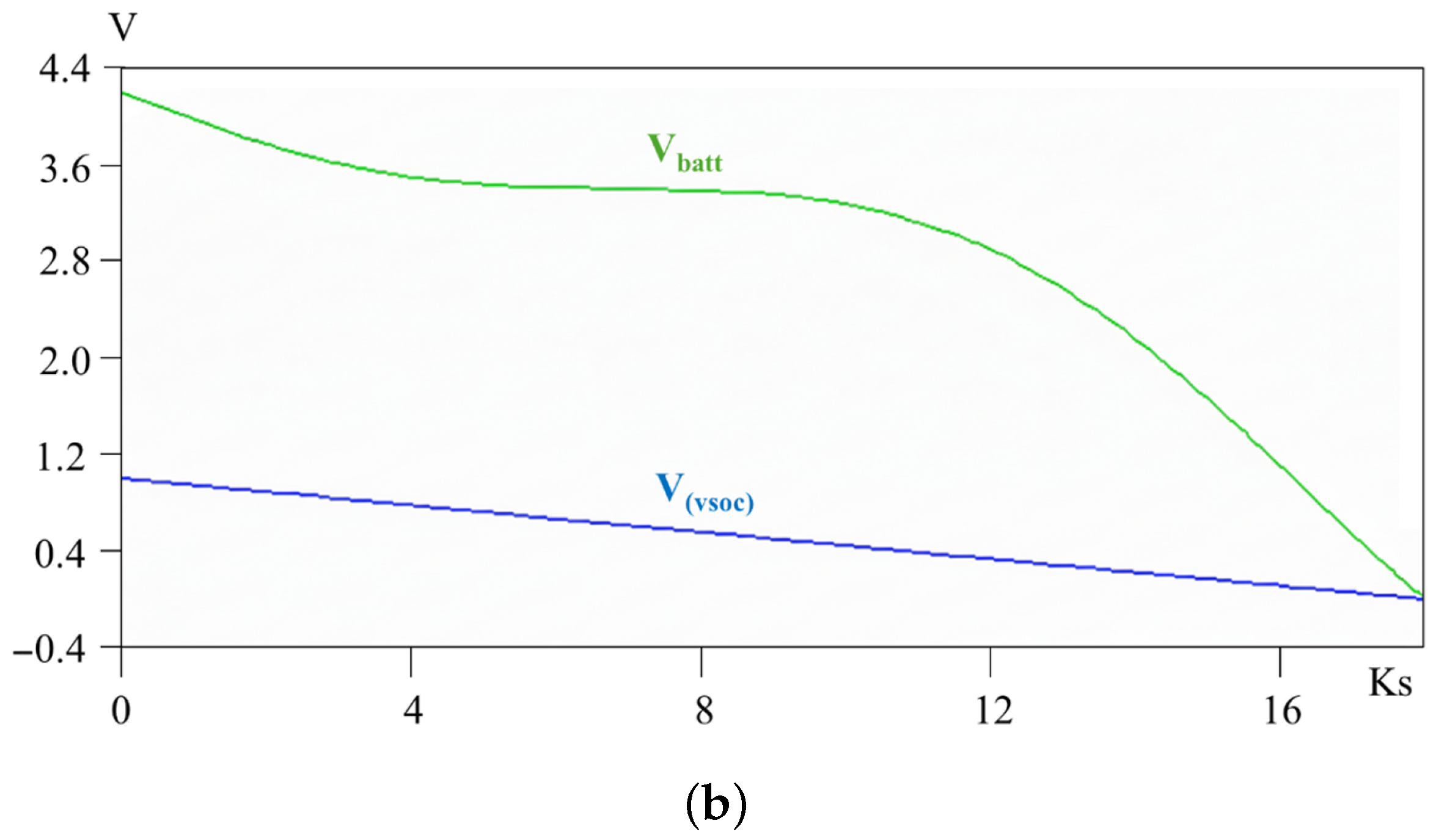
Figure 3. (a) Final circuit implemented in LTspice. (b) Characteristic curve obtained in LTspice.
Computation 14 00061 g003aComputation 14 00061 g003b
Figure 4. (a) CTPTC topology. (b) Active balancing unit.
Computation 14 00061 g004aComputation 14 00061 g004b
Figure 5. Acquisition system.
Computation 14 00061 g005
Figure 6. Conditioning and acquisition stages: (a) Front-end and first stage of multiplexers for voltage acquisition. (b) Second stage of multiplexers and signal conditioning prior to the ADC.
Computation 14 00061 g006
Figure 7. Symmetric source.
Computation 14 00061 g007
Figure 8. Front-end of the current shunt.
Computation 14 00061 g008
Figure 9. Temperature acquisition, bidirectional gate stage of MOSFETs, and gate control. (a) PT100 signal conditioning and acquisition by ADC. (b) Bidirectional MOSFET gate (The symbol ** represents exponentiation ^, and the symbol * represents single multiplication). (c) High-speed voltage comparator.
Computation 14 00061 g009
Figure 10. Response curves of the GNL equivalent circuit model: (a) VSOC vs. Time. (b) OCV vs. Time. (c) VSOC vs. OCV vs. Time.
Computation 14 00061 g010aComputation 14 00061 g010b
Figure 11. Response to sweeping over MUX stages, the area shaded in red is outside of the allowed tolerances. (a) Voltage MUXs. (b) Temperature MUXs.
Computation 14 00061 g011
Figure 12. Response per channel to voltage, current, and temperature signals. (a) Voltage and current channel. (b) Cell temperature channel.
Computation 14 00061 g012
Figure 13. Response speed of the cutoff comparator with a current transient.
Computation 14 00061 g013
Figure 14. System efficiency in balancing and unloading mode.
Computation 14 00061 g014
Table 1. Comprehensive BMS validation: requirements, standards, and test criteria.
Testing RequirementStandards/GuidelinesTest DescriptionEnd-of-Test Criteria
Overcharge Control (Voltage and Current)IEC 62619 UL 1973, UL 9540 NAVSEA S9310Inject current > nominal limit and force cell voltages above safety threshold (e.g., >4.2 V).The BMS detects excess V/I and disconnects the charger immediately.
Over-Discharge Control (Voltage and Current)UL 1973, UL 9540 NAVSEA S9310Apply load > peak current limit; discharge until weakest cell hits cutoff (e.g., 2.5 V).BMS disconnects load to prevent thermal stress or degradation.
Overheating ControlIEC 62619Apply high-stress cycling or external heat to simulate thermal runaway precursors.BMS detects temperature rise and disconnects before critical limit.
Cell BalancingIEEE 1679.1Verify active/passive algorithm execution under induced SoC imbalance.Voltage difference ( Δ V ) reduced below target (e.g., <10 mV).
DisconnectionIEEE 1679.1Test main contactor disconnection and HV bus isolation under fault conditions.Contactors open; terminal voltage drops to zero.
Cell Operating RangeIEC 62619 UL 1973, UL 9540 IEEE 1679.1Verify measurement accuracy across the full Safe Operating Area (SOA).Readings remain within accuracy tolerance across the range.
Temperature RangeIEEE 1679.1Thermal chamber testing across full operational range (e.g., −20 to 60 °C).Correct operation without false trips or communication loss.
Thermal ManagementIEEE 1679.1 UL 1973, UL 9540Validate activation of cooling/heating systems at set temperature thresholds.Systems activate and regulate pack temperature successfully.
Heating and CoolingIEEE 1679.1Assess regulation response speed during rapid thermal cycling.Actuators respond within required time delay.
Thermal FaultIEEE 1679.1Simulate sensor failure (open/short) or localized hot spots.BMS detects fault and enters safe/shutdown mode.
Short CircuitNAVSEA S9310Apply low-impedance shorts at terminals and internal busbars.Current interrupted instantly; drops to zero.
Functional SafetyIEC 62619 UL 1973, UL 9540Verify self-diagnosis, redundancy, and fail-safe logic (e.g., watchdog).System defaults to safe state upon failure detection.
Disclaimer/Publisher’s Note: The statements, opinions and data contained in all publications are solely those of the individual author(s) and contributor(s) and not of MDPI and/or the editor(s). MDPI and/or the editor(s) disclaim responsibility for any injury to people or property resulting from any ideas, methods, instructions or products referred to in the content.