Article

Co-Design of the Control and Power Stages of a Boost-Based Rectifier with Power Factor Correction Depending on Performance Criteria

by
Carlos Andres Ramos-Paja
1,*,†,
Andres Julian Saavedra-Montes
1,† and
Juan David Bastidas-Rodriguez
2,†
1
Facultad de Minas, Universidad Nacional de Colombia, Medellin 050013, Colombia
2
Facultad de Ingeniería y Arquitectura, Universidad Nacional de Colombia, Manizales 170003, Colombia
*
Author to whom correspondence should be addressed.
These authors contributed equally to this work.
Computation 2022, 10(4), 61; https://doi.org/10.3390/computation10040061
Submission received: 23 February 2022 / Revised: 30 March 2022 / Accepted: 1 April 2022 / Published: 11 April 2022
(This article belongs to the Section Computational Engineering)

Abstract

:
Rectifiers with power factor correction are key devices to supply DC loads from AC sources, guaranteeing a power factor close to one and low total harmonic distortion. Boost-based power factor correction rectifiers are the most widely used topology and they are formed by a power stage (diode bridge and Boost converter) and a control system. However, there is a relevant control problem, because controllers are designed with linearized models of the converters for a specific operating point; consequently, the required dynamic performance and stability of the whole system for different operating points are not guaranteed. Another weak and common practice is to design the power and control stages independently. This paper proposes a co-design procedure for both the power stage and the control system of a Boost-based PFC rectifier, which is focused on guaranteeing the system’s stability in any operating conditions. Moreover, the design procedure assures a maximum switching frequency and the fulfillment of different design requirements for the output voltage: maximum overshoot and settling time before load disturbances, maximum ripple, and the desired damping ratio. The proposed control has a cascade structure, where the inner loop is a sliding-mode controller (SMC) to track the inductor current reference, and the outer loop is an adaptive PI regulator of the output voltage, which manipulates the amplitude of the inductor current reference. The paper includes the stability analysis of the SMC, the design procedure of the inductor to guarantee the system stability, and the design of the adaptive PI controller parameters and the capacitor to achieve the desired dynamic performance of the output voltage. The proposed rectifier is simulated in PSIM and the results validate the co-design procedures and show that the proposed system is stable for any operating conditions and satisfies the design requirements.

1. Introduction

Rectifiers, or AC/DC converters, are essential electronic devices to feed DC loads from AC sources. In fact, most of the DC loads used in residential or industrial applications include rectifiers to generate the required DC voltage from the grid. Typical rectifiers are constructed with a diode or thyristor bridge and a capacitor to generate an approximately constant voltage to supply the power required by the load. Although those rectifiers are simple and low cost, they produce large distortions in the current provided by the AC source, since a typical rectifier, even with an ideal resistor as load, is a highly nonlinear load from the AC source point of view [1,2]. Those nonlinear loads are translated into a significant increment of the Total Harmonic Distortion (THD) of the AC sources, they negatively affect the load power factor (PF), produce imbalances in the three-phase systems, and, as consequence, it is not possible to utilize the full energy potential from the grid nor meet power quality standards such as IEC 61000-2-3 [3] and IEEE 519 [4].
One option to supply a DC load from an AC source with low-input current distortions (i.e., low THD) and PF close to one are the rectifiers with active power factor correction (PFC), which are usually formed by a diode bridge, a DC/DC power converter, and a control system [1,2]. Even if those devices introduce higher system complexity and higher costs, regarding traditional rectifiers, the joint operation of the DC/DC converter and the control system can cause the rectifier to behave as a resistive load from the AC source perspective. Hence, the PF is close to one, the THD is significantly improved, and there is a reduction in the three-phase system imbalances; all of this allows the increment of the power drawn from the grid. Additionally, these devices can be used for different power levels and allow the compliance of power quality standards [1,2].
PFC rectifiers can be implemented with different DC/DC converter topologies such as Boost, Buck [5], Buck-Boost [6], Cuk [7], Sepic [8], and Flyback [9], among others. However, Boost-based PFC rectifiers are the most widely adopted topology in the literature, since the Boost converter provides continuous input current, requires few elements (i.e., low cost), has a simple model, and has a simpler analysis and control design than Cuk- and SEPIC-based rectifiers [1,2]. Additionally, Boost converters are also extensively used in a high variety of applications, from motor drives [10] to microgrids [11]. Therefore, this paper considers a Boost-based PFC rectifier to propose a co-design procedure for both converter and control strategy.
In Boost-based PFC, the control problem is to regulate the DC output voltage ( v d c ) to a constant reference ( v r ) with zero steady-state error considering a time-varying input voltage ( v i n = v p k · | sin ( w · t ) | ) as well as perturbations in the DC load current ( i d c ) and the peak input voltage ( v p k ): where v i n is the input voltage, w is the angular frequency, and t is the time. Table 1 summarizes the main perturbations and their main causes and effects on v d c . Although the typical control structure for widely used power converters, such as Buck and Boost, is aimed at regulating their output voltage with a single loop [12,13], the most common structure to tackle this control problem is a cascade controller, where the outer loop regulates the DC output voltage ( v d c ) to a constant reference ( v r ) by modifying the amplitude of the inductor current reference ( i r ), while the inner loop tracks i r acting on the Boost switch [1]. Moreover, i r must be in phase with the converter input voltage ( v i n ), which corresponds to the output of the diode bridge, i.e., v i n = v p k · | sin ( w · t ) | ; hence, i r is defined as i r = i p k · | sin ( w · t ) | , where w is the angular frequency of the AC source.
The outer loop is typically implemented with a PI controller, either with analog [1,14,15,16,17] or digital circuitry [18,19,20], since it rejects load perturbations, it provides zero steady-state error, and its parameters can be tuned by frequency response [16,19]. Moreover, the PFC system regulated by a PI controller is relatively simple because the inner loop deals with the system nonlinearities and the time-varying reference. Nevertheless, in many cases the design procedure of the PI controller of the outer loop is not provided [14,15,18,20] or it is not clearly explained [16,17,19].
The inner loop can be implemented with linear or nonlinear controllers to track i r . Linear controllers such as P [19] and PI [17] are commonly used to track i r in PFC rectifiers. These controllers are simple, can be implemented with analog circuits or microcontrollers, and can be tuned with different methods, such as frequency response [17,19]. However, in many works, the authors do not provide a clear design method for the linear controllers [16,17,19], and those controllers are designed and tuned with linearized models of the DC/DC converter in a particular operating point; therefore, they cannot guarantee the desired dynamic performance for different loads, and the system stability may be compromised under particular operating conditions. Moreover, other works, such as the one reported in [21], use feedforward compensators to improve the dynamic response of the system. That work is based on two control loops (inner current loop and outer voltage loop), which have two adaptive gains calculated to compensate changes on the grid voltage and load current. However, that paper only considers resistive loads in its analysis and the adaptive gains have a calculation delay imposed by a peak detector, which needs half of the grid cycle to update their values. That is why sliding-mode controllers (SMC) are an interesting option for controlling Boost converters [13], since they take advantage of the converter variable structure imposed by the switch, and those controllers provide fast dynamic responses.
The authors of [18,20] propose a cascade controller for a Boost-based PFC where the outer loop is a digital PI to regulate v d c and the inner loop is an SMC to track i r . Although in both papers the switching function is defined as Ψ = i L i r (where i L is the inductor current), the authors of [18] propose a method to implement the hysteresis band on a microcontroller, while [20] uses the equivalent control analysis to calculate the converter duty cycle to generate a PWM that acts on the switch. Moreover, [20] proposes an additional loop to regulate the converter switching frequency to a desired value by modifying the hysteresis band. However, these papers do not provide a design procedure of the PI parameters and [18] do not include the stability analysis. Furthermore, the SMC proposed in [18] generates a duty cycle and not the converter switching signal, which reduces the speed of the system dynamic response.
In [15,22], the authors propose an SMC to track i r where the switching function has the following form: Ψ = k 1 · ( i L i r ) + k 2 · ( v d c v r ) . The authors of [15] do not perform the stability analysis nor provide a design procedure for k 1 and k 2 ; but they use a PI as outer loop to regulate v d c (by modifying i r ) and to guarantee zero steady-state error. While in [22] the authors perform the stability analysis of the controlled system, they propose an expression to determine the hysteresis band to assure a maximum switching frequency, and they determine the SMC parameters ( k 1 and k 2 ) by using a genetic algorithm. Unfortunately, the control structure proposed in [22] does not include an outer loop to regulate v d c , which results in steady-state error in v d c ; in addition, the optimization problem to determine k 1 and k 2 is not clearly explained.
Other works use SMC theory to propose complex controllers to track i r by generating the duty cycle of the Boost converter [14,23,24,25]. In [23], the authors propose an SMC observer for i L and v d c , and combine this observer with a triangular signal to generate a PWM with a fixed frequency. The proposed control system has four parameters: two for the SMC observer and two to define the triangular signal. Although the work [23] includes a Lyapunov-based stability analysis and defines conditions to guarantee the stability, it does not provide a methodology to design the four controller parameters and it does not regulate v d c , since no outer loop is implemented.
Moreover, the works presented in [14,24,25] use complex switching functions to implement the SMCs. In [14,24], the proposed switching functions include the inductor current error as well as its first [14] and the second integrals [24]; while in [25], the switching function considers the inductor current and output voltage errors along with their integrals. On the one hand, the advantages of the work introduced in [14] are: it combines two switching functions to provide robustness to uncertainties in the inductor resistance and inductance; it performs a Lyapunov-based stability analysis; and the controller includes a PI to regulate v d c and to provide zero steady-state error. However, one of the switching functions is not clearly defined and there is no design procedure for the PI parameters. On the other hand, the advantages of the work presented in [24] are: it provides a design procedure for the SMC parameters (based on frequency response); it performs the stability analysis using sliding-mode theory; and the SMC is implemented with a commercial PFC controller (integrated circuit). However, the controller does not include an outer loop to regulate v d c (i.e., v d c has a steady-state error), the SMC implementation with the commercial PFC integrated circuit is not clearly justified, and the experimental results show high ripples in i L .
Additionally, one of the advantages of the controller proposed in [25] is that inductor-current SMC includes the output voltage error in the switching function to improve the dynamic response and robustness of v d c , which is regulated by a PI. The other advantage is that the paper includes the stability analysis of the system and the inequalities to be considered for the design of the three switching function constants. Nevertheless, there is not a detailed design procedure for the SMC parameters to facilitate its implementation in other converters, it requires an additional sensor to measure the output capacitor current, and considers a resistive load. Further, similar to the SMC-based controllers introduced in [14,23,24,25], the SMC generates a PWM signal and not the converter-switching signal, which reduces the speed of the converter dynamic response.
Finally, the controller proposed in [26] combines the SMC and fuzzy logic control (FLC) to track the inductor current reference generated by a PI regulator of the output voltage. The SMC is used to generate one component of the duty cycle (or the equivalent control signal u e q ) considering a simple sliding surface ( Ψ = i L i r ), while the FLC uses the signal S = ( i L i r ) d ( i L i r ) / d t to generate a second component of the duty cycle ( u s ). Then, u e q and u s are combined to generate the converter duty cycle. Even though the authors validate the proposed approach with experimental results, they do not perform any stability analysis of the system nor a design procedure of the proposed controllers. Moreover, they do not provide information on the PI regulator of v d c and the SMC is not used to generate the converter switching signal.
From the papers discussed before, it is possible to identify two main points: the first one is the lack of a joint design procedure (or co-design) of the converter’s and controller’s parameters considering the system stability, and the second one is the lack of a solution for the open-loop condition when i L = 0 [ A ] . Regarding the first point, only [16] provides expressions to determine the converter’s inductor and capacitor, while [27] merely introduces an expression to define the capacitor; nevertheless, those expressions are independent of the control structure and they do not consider the system stability. Regarding the second point, in [23,24], the authors determine the region (in radians) where the system is “out-of-control” [23] or the time interval where the system is in open-loop [24]; however, these works do not propose any solution to guarantee the system stability when i L is close to zero.
Therefore, this paper proposes a co-design procedure of the control system (inner and outer loops) and the converter for a Boost-based PFC to guarantee global stability of the system even close to i L = 0 [ A ] . The proposed controller assures a PF close to one as well as v d c regulation with the desired ripple and settling time before nonlinear load perturbations. The inner loop tracks i r and it is implemented with an SMC using a simple switching function Ψ = i L i r , while the outer loop regulates v d c with an adaptive PI controller. Hence, this paper has three main contributions: (1) a cascade controller that guarantees the global stability of the system for any operating condition and considering nonlinear loads, (2) a detailed co-design procedure of the converter (L and C) and controller parameters ( k p and k i ) to ensure the system stability and the desired dynamic response (settling time, maximum overshoot, and v d c ripple), (3) a solution for the open-loop condition when i L = 0 [ A ] as well as a detailed analysis of the ripples in v d c produced by the time-varying input voltage.
The rest of the paper begins with Section 2, which includes all the details of the proposed approach including the mathematical model of the system, the design of the proposed cascade controller, the design of the inductor, and the design of the capacitor. Then, Section 3 shows the validation of the proposed approach with detailed simulation results, and Section 4 closes the paper with the discussion.

2. Materials and Methods

This section describes the proposed co-design procedure of the converter and the control system for a Boost-based rectifier with PFC. This section is divided into six subsections, where the first one (Section 2.1) introduces a control-oriented model of the system including the Boost converter and a generic load. Then, Section 2.2 presents the SMC controller of the i L along with the validation of the stability conditions (transversality, reachability, and equivalent control) and its practical implementation. Later, Section 2.3 shows the inductor design procedure to guarantee global stability in the SMC. Next, Section 2.4 introduces the design of the v d c controller and the capacitor to meet the desired dynamic response and guarantee the system stability; while Section 2.5 presents an analysis of the ripples in v d c introduced by v i n . Finally, Section 2.6 summarizes the complete co-design procedure to facilitate its implementation.

2.1. Circuital and Mathematical Models

The simplified scheme of the Boost-based rectifier with power factor correction is reported in Figure 1, where the inductor current i L of the boost converter must be regulated to be in-phase with the input voltage v i n of the converter, i.e., the output voltage of the diode–bridge rectifier. Moreover, the electrical scheme also shows the nonlinear load modeled using a current source i o ; such a model provides higher generality to the system design in comparison with resistive models usually adopted in literature to represents loads, since the current source is a suitable model to represent the power converters commonly present at the input of commercial DC loads [28,29].
The scheme of Figure 1 reports the current controller in red color, which is based on a sliding-mode controller (SMC) and a multiplier. Such a control system measures the v i n waveform, which is applied to the current reference i r of the SMC, using i w , to ensure the inductor current i L is in-phase with the input voltage v i n , thus ensuring a high power factor (PF) [1]. The peak value i p k of the current reference is defined by the voltage controller, which is depicted in blue. Such a voltage controller must be designed using an adaptive strategy to provide the same performance for any operating condition imposed by the load, i.e., for different power and current requested by the load.
The switched differential equations describing the boost converter operation are given in (1) and (2), where u represents the activation signal of the MOSFET.
d i L d t = v i n v d c · 1 u L
d v d c d t = i L · 1 u i o C
The averaged value of u within the switching period T s w corresponds to the duty cycle of the converter, i.e., d = 1 / T s w · 0 T s w u d t , hence, the averaged model of the converter is the following one:
d i L d t = v i n v d c · 1 d L
d v d c d t = i L · 1 d i o C
Finally, the steady-state relations of the converter are obtained from (3) and (4) by considering the differential equations equal to 0, which lead to:
1 d = v i n v d c = i o i L

2.2. Current Controller

The current controller is designed using the sliding-mode theory, hence it corresponds to an SMC. The sliding-mode theory is adopted since it provides robustness to parametric changes [30,31], which is useful to overcome aging or tolerance effects. Moreover, the SMC provides a binary output, which matches the binary nature of the control signal u needed to activate or deactivate the MOSFETs of the DC/DC converter.
The proposed SMC is based on the sliding-surface Φ reported in (6), where Ψ (7) is the switching function defining the surface. The operation of the system into that surface Φ forces the inductor current i L to follow the reference i r . In that way, it is possible to impose a sinusoidal waveform into i L to ensure the desired power factor for the rectifier.
Φ = Ψ = 0
Ψ = i L i r
The analysis of the SMC stability is based on three tests: the transversality condition, the reachability conditions, and the equivalent control [32,33].

2.2.1. Transversality Condition

The transversality condition evaluates the ability of the controller to modify the system trajectory. Therefore, the control signal u must be present into the trajectory derivative. This is formalized as follows:
d d u d Ψ d t 0
The previous condition is fulfilled when the control signal u is present into the derivative of the switching function Ψ . Therefore, the first step of this analysis is to obtain the switching function derivative as follows:
d Ψ d t = d i L d t d i r d t
Replacing the switching expression of d i L d t given in (1) into (9) leads to:
d Ψ d t = v i n v d c · 1 u L d i r d t
Finally, replacing expression (10) into (8) provides the final transversality proof given in (11), which is always different from zero since v d c and L are positive values. Therefore, it is confirmed that the SMC based on (7) and (6) is feasible.
d d u d Ψ d t = v d c L > 0

2.2.2. Reachability Conditions

The reachability conditions test the ability of the SMC to drive the system to the surface and keep operating inside that desired surface. The reachability conditions are the following ones [32,33]:
  • When the system ( Ψ ) is operating under the surface ( Ψ < 0 ), the derivative of the switching function must be positive to reach the surface:
    lim Ψ 0 d Ψ d t > 0
  • When the system ( Ψ ) is operating above the surface ( Ψ > 0 ), the derivative of the switching function must be negative to reach the surface:
    lim Ψ 0 + d Ψ d t < 0
However, the transversality sign also impacts the test of the reachability conditions: a positive transversality sign implies that positive changes on the control signal u produce positive switching function derivatives ( d Ψ d t > 0 ); on the contrary, a negative transversality sign implies that positive changes on the control signal u produce negative switching function derivatives ( d Ψ d t < 0 ). Taking into account that the transversality sign is always positive (11), the reachability conditions that must be tested for this case are:
lim Ψ 0 d Ψ d t u = 1 > 0
lim Ψ 0 + d Ψ d t u = 0 < 0
Replacing the explicit equation for the switching function derivative (10) into both reachability conditions gives:
v i n v d c L < d i r d t < v i n L
The previous expressions provide the conditions on d i r d t and L that must be fulfilled to ensure the reachability conditions, which also guarantee the controller stability. In Section 2.3, the expression for d i r d t will be analyzed to calculate a design equation for L, which guarantees that the reachability conditions are always fulfilled.

2.2.3. Equivalent Control Condition

In DC/DC converter applications, the equivalent control condition evaluates the saturation of the duty cycle d [32]. In general, the equivalent control condition is the following one: the averaged value of the control signal u must be always constrained by the possible values of that signal. In DC/DC converters, the possible values of u are 1 (MOSFET closed) and 0 (MOSFET open); moreover, the averaged value of u corresponds to the converter’ duty cycle d. Therefore, when the equivalent control condition is fulfilled, the DC/DC converter operates with a duty cycle inside the physical limits ( 0 < d < 1 ) to avoid instability caused by duty cycle saturation.
Since the reachability conditions ensures that the SMC drives the system to the sliding-surface, the equivalent control condition is evaluated inside the surface:
Ψ = 0 d Ψ d t = 0
The first step of this test is to obtain the expression for the control signal u when the system is operating inside the sliding surface:
u = 1 v i n L · d i i r d t v d c
Then, such an expression is averaged as d = 1 / T s w · 0 T s w u d t , and the result is constrained into 0 < d < 1 , which results in the same expression previously reported in (16). Therefore, this test confirms that fulfilling the condition given in (16) also ensures the equivalent control condition, i.e., the duty cycle is not saturated.
Finally, the three tests confirm that the proposed SMC is stable when condition (16) is fulfilled; hence, the inductor current i L follows the reference value i r .

2.2.4. Practical Implementation

The proposed SMC requires a control law to be implemented. Such a control law is extracted from the reachability conditions: from (14) it is observed that the control signal must be set to u = 1 when Ψ < 0 , while (15) indicates that u = 0 when Ψ > 0 . However, theoretical sliding-mode controllers require infinite switching frequency F s w , which is impossible to implement [32]. Therefore, SMCs are traditionally implemented using an hysteresis band ± Δ Ψ around the sliding surface to limit the switching frequency:
Ψ = 0 Ψ Δ Ψ
The previous hysteresis band requires the following practical control law, which is an extension of the theoretical control law extracted from the reachability conditions:
u = 1 if Ψ < Δ Ψ 0 if Ψ > + Δ Ψ
The current reference i r changes at the grid frequency, which is much smaller than the switching frequency (60 Hz vs. 250–300 kHz). Therefore, with a switching period T s w (less than 5 μ s) the changes on i r are almost negligible; hence, the hysteresis limit Δ Ψ is equal to the inductor current ripple Δ i L . Such a relation is obtained from (7) as follows:
Δ Ψ = Δ i L because Δ i r 0 within T s w
From Equation (1), the inductor current ripple is calculated as given in (22), which leads to the switching frequency expression given in (23).
Δ i L = v i n · d · T s w 2 · L = Δ Ψ
F s w = v i n · d 2 · L · Δ Ψ
Figure 2 illustrates the effect of the hysteresis band on the switching frequency, where the Ψ waveform is constrained within Δ Ψ , + Δ Ψ . The figure at the top shows that reducing Δ Ψ increases F s w , this because the Ψ waveform requires a shorter time to complete a period (higher F s w ), which is in agreement with Equation (23).
Similarly, the bottom traces of Figure 2 shows the effect of the inductance L in the switching frequency: reducing L increases the derivative of the inductor current, as given in (1); hence, the Ψ waveform takes a shorter time to reach the hysteresis band (higher F s w ), which is also in agreement with Equation (23).
Finally, the switching function Ψ must be always inside the hysteresis band Δ Ψ , + Δ Ψ to ensure that the inductor current i L follows the reference value i r . Otherwise, when Ψ is outside Δ Ψ , + Δ Ψ the inductor current is not regulated; consequently, the power factor correction is not ensured. Therefore, both L and Δ Ψ values must be carefully designed.

2.2.5. SMC Circuit

The circuital implementation of the SMC is performed using the control law previously defined in (20). Such an implementation uses two traditional comparators to test the inequalities of the control law, and a flip-flop S-R is used to set the control signal u according to (20): SET (S) = 1 imposes the output Q (u) = 1; while RESET (R) = 1 imposes Q (u) = 0. Finally, the switching function Ψ is calculated using a subtractor as given in (7). Figure 3 summarizes the circuital implementation of the SMC, which is commonly constructed using operational amplifiers and a TS555-integrated circuit [34,35].

2.3. Design of the Inductor to Guarantee Global Stability

The inductor L must be designed to ensure that the reachability conditions (16) are fulfilled, otherwise the global stability of the SMC will not be guaranteed. From Figure 1, it is observed that i r must have the same waveform (frequency and phase) that the input voltage v i n to ensure a unitary power factor, but the peak value i p k of the current reference is defined by the voltage controller to regulate the DC voltage as v d c = v r .
The input voltage of the converter, i.e., the output voltage of the diode rectifier, has a waveform defined in (24), where v p k is the peak value of the voltage and f g is the grid frequency ( T g = 1 / f g ) is the period of the grid). Therefore, in general, the current reference has the form given in (25), where i p k is the peak current.
v i n = v p k · sin 2 · π · f g · t for 0 t T g / 2
i r = i p k · sin 2 · π · f g · t for 0 t T g / 2
To evaluate the conditions in (16) it is necessary to calculate the expression for the derivative of i r :
d i r d t = 2 · i p k · π · f g · cos 2 · π · f g · t
The previous expressions will be analyzed in the interval 0 t T g / 2 , since those signals have the same values in the interval T g / 2 t T g due to the action of the diode bridge rectifier. Replacing expressions (24) and (26) into (16) leads to:
v p k · sin 2 · π · f g · t v d c L < 2 · i p k · π · f g · cos 2 · π · f g · t
2 · i p k · π · f g · cos 2 · π · f g · t < v p k · sin 2 · π · f g · t L
Taking into account that the boost converter requires an input voltage smaller than the output voltage, i.e., v i n < v d c , condition (27) is fulfilled since the left term is always negative and the right term is positive in the analysis interval. In contrast, condition (28) could not be fulfilled when the right side of the expression becomes very small, which occurs when the input voltage v i n and grid voltage v g are near to zero. Therefore, such a condition must be analyzed in detail: it is observed that expression (28) corresponds to the reachability condition given in (14), where the switching function derivative has the following form:
d Ψ d t u = 1 = v p k · sin 2 · π · f g · t L 2 · i p k · π · f g · cos 2 · π · f g · t
Then, the explicit expression for the changes of Ψ is obtained by integrating Equation (29), as follows:
Ψ = v p k 2 · π · f g · L cos 2 · π · f g · t + i p k · sin 2 · π · f g · t
The maximum amplitude of Ψ when expression (28) is not fulfilled ( v i n near to zero) occurs at d Ψ d t u = 1 = 0 ; then, the time t = T x when such a condition occurs is evaluated from expression (29):
T x = T g 2 · π · arctan 2 · π · f g · L · i p k v p k
Such a maximum amplitude of Ψ is calculated by evaluating Equation (30) for t = T x :
max Ψ = v p k 2 · π · f g · L 1 + 1 + 2 · π · f g · L · i p k v p k 2 for u = 1
The previous section described that global stability is ensured when the maximum deviation of the switching function is always trapped inside the hysteresis band; therefore, the inductance L must be designed to ensure the following stability condition:
max Ψ Δ Ψ
Figure 4 illustrates the waveform of Ψ when the system approaches v i n 0 , i.e., not fulfilling (28), for two values of L: with L 1 the stability condition (33) is not fulfilled, hence i L does not follow closely the reference i r during a section of the grid period, thus degrading the power factor; instead, with L 2 the stability condition (33) is always fulfilled, hence i L follows closely i r for all the grid period, thus providing a high power factor.
Figure 4 indicates that L 1 > L 2 , which is confirmed by calculating the partial derivative of max Ψ with respect to L, as given in (34), which is always positive. Therefore, increasing L also increases max Ψ .
max Ψ L = v p k 2 · π · f g · L 2 1 1 1 + 2 · π · f g · L · i p k v p k 2 > 0 for u = 1
Finally, operating (32) and (33), the inductance values that fulfill the reachability conditions are calculated using (16), ensuring global stability of the SMC even when v i n is near zero.
L v p k · Δ Ψ π · f g i p k 2 Δ Ψ 2
Figure 1 shows that i p k is provided by the voltage controller; hence, the worst-case condition for i p k is calculated in the following sections.

2.4. Voltage Controller and Capacitor Design

The voltage controller and bus capacitor must be designed to impose the average DC voltage v d c required by the load. This process requires the converter behavior to be modeled under the action of the current controller. Therefore, the following section presents the equivalent dynamics of the current loop and the proposed voltage loop.

2.4.1. Equivalent Model of the Current and Voltage Loops

Taking into account that the current SMC is globally stable, the sliding surface (6) ensures that i L = i r . Therefore, the voltage differential Equation (4) of the averaged model is modified as given in (36), where v d c is the averaged DC voltage at the converter output, and i r represents the averaged value of the current reference. Finally, Equation (37) reports the Laplace representation of the averaged DC voltage v d c ( s ) for changes on the average value of reference i r ( s ) and the load current i o ( s ) .
d v d c d t = i r · 1 d i o C
v d c ( s ) = i r ( s ) · 1 d i o ( s ) s · C
Figure 5 presents the voltage loop proposed to regulate the DC voltage. In such a figure the block G V represents the voltage controller, which will be designed in the Laplace domain.
The previous diagram enables to calculate the following closed-loop expression for the average DC voltage:
v d c ( s ) = G V · 1 d s · C + G V · 1 d · v r 1 s · C + G V · 1 d · i o ( s )

2.4.2. Adaptive Controller Design

The proposed voltage controller is given in (39), which corresponds to a proportional-integral (PI) structure.
G V = k p + k i s
In these kinds of applications, the reference value is usually constant; hence, the changes on v d c ( s ) are caused by perturbation on the load current i o ( s ) . Therefore, the transfer function G d c / o ( s ) between i o ( s ) and v d c ( s ) is calculated from (38) and (39) as given in (40).
G d c / o ( s ) = v d c ( s ) i o ( s ) = 1 s · C + G V · 1 d = s C s 2 + 1 d k p C s + 1 d k i C
The main problem of such a model concerns the dependency on the duty cycle d, which changes depending on the operating point as reported in (5); hence, the values of k p and k i will produce a different performance for different i o . Therefore, this paper proposes to adapt the k p and k i values depending on the operating point defined by d; this is performed by using the following normalized parameters x p and x i :
x p = 1 d k p x i = 1 d k i
Then, expression (40) is rewritten using x p and x i as follows:
G d c / o ( s ) = s C s 2 + x p C s + x i C
The objective is to calculate those x p and x i values to impose the desired performance in any operating conditions. The performance is defined by the following criteria:
  • The reference v r for the averaged DC voltage is constant.
  • The load current i o is the main perturbation for the average DC voltage. This design is performed for the worst-case scenario, which corresponds to a step change in the load current as given in (43), where I o is the step size.
    i o ( s ) = I o s
  • The maximum deviation allowed for the average DC voltage is M O d c .
  • The maximum settling time (2% criterion) for recovering the average DC voltage is t s .
  • The waveform of the average DC voltage must have a damping ratio ρ .
Considering the step function of the load current given in (43), the average DC voltage has the following Laplace representation, in which I o is a scalar.
v d c ( s ) = I o C s 2 + x p C s + x i C
Taking into account that the canonical form of a second order system ω n 2 s 2 + 2 · ρ · ω n · s + ω n 2 has a settling time t s , c = ln ϵ ρ · ω n ; then, the values of x p and x i to ensure a damping ratio ρ and a 2% settling time t s to the average DC voltage are:
x p = 2 · ln ϵ · C t s , ϵ = 0.02
x i = ln ϵ ρ · t s 2 · C
From Figure 1, it is observed that the adaptive voltage controller must define only the peak current i p k of the SMC reference i r , since the current waveform i w is a normalization of the input voltage (over the peak voltage v p k ) to ensure a high power factor. Therefore, such a peak current i p k must ensure the average reference current i r corresponds to the value defined by the G V adaptive controller. This process requires the calculation of the average value of i r from (25) as i r = 2 · i p k π , which leads to the following peak value:
i p k = π 2 · i r
Hence, the output of the G V adaptive controller must be multiplied by π 2 to ensure the desired average current extracted from the diode bridge rectifier. Moreover, the x p and x i values must be denormalized in real-time, dividing them by 1 d , which provides k p and k i parameters adapted to the operation condition. The structure of the adaptive voltage controller is summarized in Figure 6: the controller measures v d c and v i to calculate 1 d , which is used to calculate the k p and k i parameters; moreover, the averaged value of the DC voltage ( v d c ) is calculated using a low-pass filter. Finally, the structure also shows the construction of the SMC reference i r from the normalized waveform i w and the peak current i p k .

2.4.3. Capacitor Design to Ensure the Average Voltage Deviation M O d c

Another important parameter to ensure the maximum deviation M O d c of the averaged DC voltage is the capacitance C. The design of such a parameter is performed using the time-domain waveform v d c ( t ) of the averaged DC voltage, given in (48), which is obtained from the inverse Laplace transformation of (44).
v d c ( t ) = I o C x p 2 · C 1 ρ 2 1 · exp x p 2 · C · t · sin x p 2 · C 1 ρ 2 1 · t
The maximum deviation M O d c occurs when the derivative of (48) is equal to zero, which is named time t m and it is calculated in (49). Then, evaluating v d c ( t ) in (48) for t = t m leads to the M O d c expression reported in (50).
d v d c ( t ) d t = 0 t m = arctan 1 ρ 2 1 x p 2 · C 1 ρ 2 1
M O d c = 2 · I o · ρ x p · exp arctan 1 ρ 2 1 1 ρ 2 1
Finally, replacing the x p value given in (45) into (50) enables to calculate the capacitance values that ensures the limit value M O d c is not violated:
C I o · ρ · t s ln ϵ · M O d c · exp arctan 1 ρ 2 1 1 ρ 2 1
In conclusion, values of C higher than the limit defined in (51) will produce maximum deviations of the average DC voltage lower than the limit M O d c .

2.5. Low-Frequency Ripple in the DC Voltage

The operation of any single-phase rectifier produces a low-frequency ripple at the DC output. This is caused by the capacitor current generated by the interaction between the ac current extracted from the grid and the DC current requested by the load. Figure 7 shows a simplified model of the converter output port, where the diode is modeled using a current source imposing an average rectified current.
From the previous circuital scheme it is observed that the capacitor current is i C = 1 d · i p k · sin 2 · π · f g · t i o , and replacing the values of d and v i n given in (5) and (24) leads to the following expression:
i C = v p k · i p k v d c · sin 2 2 · π · f g · t i o
Stable DC voltage implies the capacitor fulfills the charge balance principle, i.e., the average capacitor current is zero in the complete grid period 0 , T g ; therefore, the steady-state relation between the load current i o and the peak values is obtained as follows:
1 T g · 0 T g v p k · i p k v d c · sin 2 2 · π · f g · t i o d t = 0 i o = v p k · i p k 2 · v d c
Then, replacing that i o expression into (53) leads to the explicit expression of i C given in (54). Figure 8 shows the waveform of i C described by Equation (54). In addition, the capacitor voltage waveform v d c , imposed by i C , is given by v d c = 1 C · i C d t ; moreover, the instants in which i C = d v d c d t = 0 correspond to the maximum and minimum values of v d c . Those instants are calculated by solving i C = 0 as t = T g 8 and t = 3 · T g 8 , and those instants are depicted in Figure 8. Since i C is a sinusoidal waveform centered in 0, i C is only positive (or only negative) between the i C = 0 points; in the example of Figure 8 i C is positive; hence, v d c is monotonically increased from the minimum value to the maximum value of the ripple.
i C = v p k · i p k v d c · sin 2 2 · π · f g · t 1 2
Taking into account that the average value v d c of v d c is at the center of the waveform, the voltage ripple is defined as ± Δ v d c around v d c . Therefore, 2 · Δ v d c = 1 C · T g / 8 3 · T g / 8 i C d t , which leads to the following ripple magnitude at the DC voltage:
Δ v d c = v p k · i p k 8 · π · f g · C · v d c
Finally, expression (56) can be used to calculate the capacitor C to ensure a maximum ripple magnitude Δ v d c , where i p k is replaced by the expression obtained in (53), where I o , m a x is the maximum steady-state value at the load current i o .
C I o , m a x 4 · π · f g · Δ v d c

2.6. Design Procedure and Application Example

This section is focused on providing a synthesis of the design procedure, which is illustrated using an application example. Figure 9 shows a scheme of the application example, which considers an isolation transformer between the ac grid and the power system for protection purposes [36]. In this example the turn-ratio of the transformer is 2:1, but such a relation can be modified depending on the application requirements. The orange block (controlled boost converter) in Figure 9 corresponds to the device to be designed, which encloses the power stage and control loops detailed in Figure 1.
The grid voltage in this application is 120 VAC, hence, the peak voltage at the transformer secondary side is v p k = 84.85 V and the grid frequency is f g = 60 Hz. The required DC voltage for the load is v d c = 220 V; such a load request has a maximum current I o , m a x = 2 A, including dynamic step-like changes with amplitudes I o = 1 A. The maximum acceptable voltage ripple at the DC side, to ensure a correct load operation, is Δ v d c = 4 V. Similarly, the correct operation of the load requires a maximum deviation of the average voltage lower than M O d c = 10 V with a 2% settling time shorter than t s , 2 % = 100 ms. This application considers a damping ratio ρ = 0.707 to provide a trade-off between response time and oscillations, and the maximum switching frequency ( F s w , m a x ) is set to F s w = 300 kHz due to the limitations of average semiconductors. Table 2 summarizes the application parameters.

2.6.1. Design of the Inductor and Hysteresis Band

The first step is to design the indictor L and hysteresis band Δ Ψ to ensure both global stability and maximum switching frequency. Those parameters are governed by Equations (23) and (35). The maximum F s w value is obtained at the maximum value of v i n , which corresponds to v p k and d = v p k / v d c 1 . Similarly, the i p k value on the stability Equation (35) is calculated as given in (53) using I o , m a x . Then, the system of equations formed by the parameterized versions of (23) and (35) is solved to establish the values fulfilling both maximum switching frequency and global stability, which can be done using any numerical method. Figure 10 shows the solution of such an equation system, where four zones are observed:
  • Left zone: a zone where Equation (35) is fulfilled, thus the system is stable, but the switching frequency is higher than 300 kHz.
  • Right zone: a zone where Equation (23) ensures F s w 300 kHz, but the system is unstable.
  • Bottom zone: a zone where the system is unstable and F s w > 300 kHz.
  • Top zone: a zone where both global stability and and F s w 300 kHz are ensured.
Therefore, any point inside the Top zone is acceptable (global stability and F s w 300 kHz). For this application example, Figure 10 was constructed by defining two vectors ( L v and Δ Ψ v ) of possible values of inductance (from 550 μ H to 950 μ H with steps of 1 μ H) and Δ Ψ (from 0.09 A to 0.15 A with steps of 100 μ A). The next step is to generate the matrix F s w , m by evaluating (23) for the possible combinations of L v and Δ Ψ v , which is used to identify the region where the switching frequency is lower or equal than F s w , m a x (300 kHz). Moreover, the stability condition (35) is evaluated for each possible combination of L v and Δ Ψ v elements, which serves to determine the regions where the system is stable or unstable. Finally, Figure 10 is the result of plotting F s w , m in the region where the system is stable and the switching frequency is lower than or equal to 300 kHz. For this example, a point at the frontier of that zone is selected to define a maximum switching frequency equal to 300 kHz, but any other one can be used; the particular point is L = 770 μ H , Δ Ψ = 113 mA .

2.6.2. Design of the Capacitor and Controller Parameters

The next step is to design the capacitor of the power stage. This process is performed using Equation (51) to ensure an average voltage deviation smaller than M O d c , and using Equation (56) to ensure a voltage ripple lower than Δ v d c at the DC side. Both expressions provide the minimum C value needed to fulfill M O d c and Δ v d c conditions; thus, a capacitor higher than the result of both equations must be selected.
Figure 11 shows the equations for calculating both M O d c and Δ v d c (solid lines), and the zones in which the average voltage deviation and voltage ripple are below the design parameters defined in Table 2. In this application example, C 663.15 μ F is needed to fulfill the desired maximum Δ v d c , according to (56); while C 823.62 μ F is required to meet the M O d c restriction given by (51); therefore, in this particular case, the limit imposed by (51) is the most restrictive condition. For this example, the value C = 827 μ F is selected inside both zones, which provides M O d c = 9.96 V and Δ v d c = 3.2 V, thus fulfilling the restrictions given in Table 2.
With the previous capacitance value, and the parameters of Table 2, expressions (45) and (46) are used to calculate the normalized parameters of the adaptive voltage controller x p = 0.0645 and x i = 2.5165 .

2.6.3. Summary of the Design Process

The design process is summarized in the flowchart depicted in Figure 12, where the processes to design the power and control stages are clearly described. The flowchart also shows that both processes can be performed in parallel due to the separability of the equations involved in those calculations.
The previous flowchart put into evidence the simplicity of the design process needed to parameterize the proposed rectifier with power factor correction; hence, providing a simple-to-use solution for real-world applications.
At this point, it is important to remark on the main contributions of the proposed control system and the co-design procedure described in this section. The first one is that the control-oriented mathematical model considers a generic model for the load, which allows the representation of nonlinear loads in the rectifier. The second contribution is the design procedure of the SMC hysteresis band ( Δ Ψ ) and the converter inductance (L) to guarantee the global stability of the SMC. The third contribution is the design procedure of the converter capacitance (C) that meets the desired maximum overshoot and maximum ripple of v d c . The last contribution is the adaptive PI to regulate v d c , where the time-varying gains k p and k i ensure the desired damping ratio and settling time.

3. Results

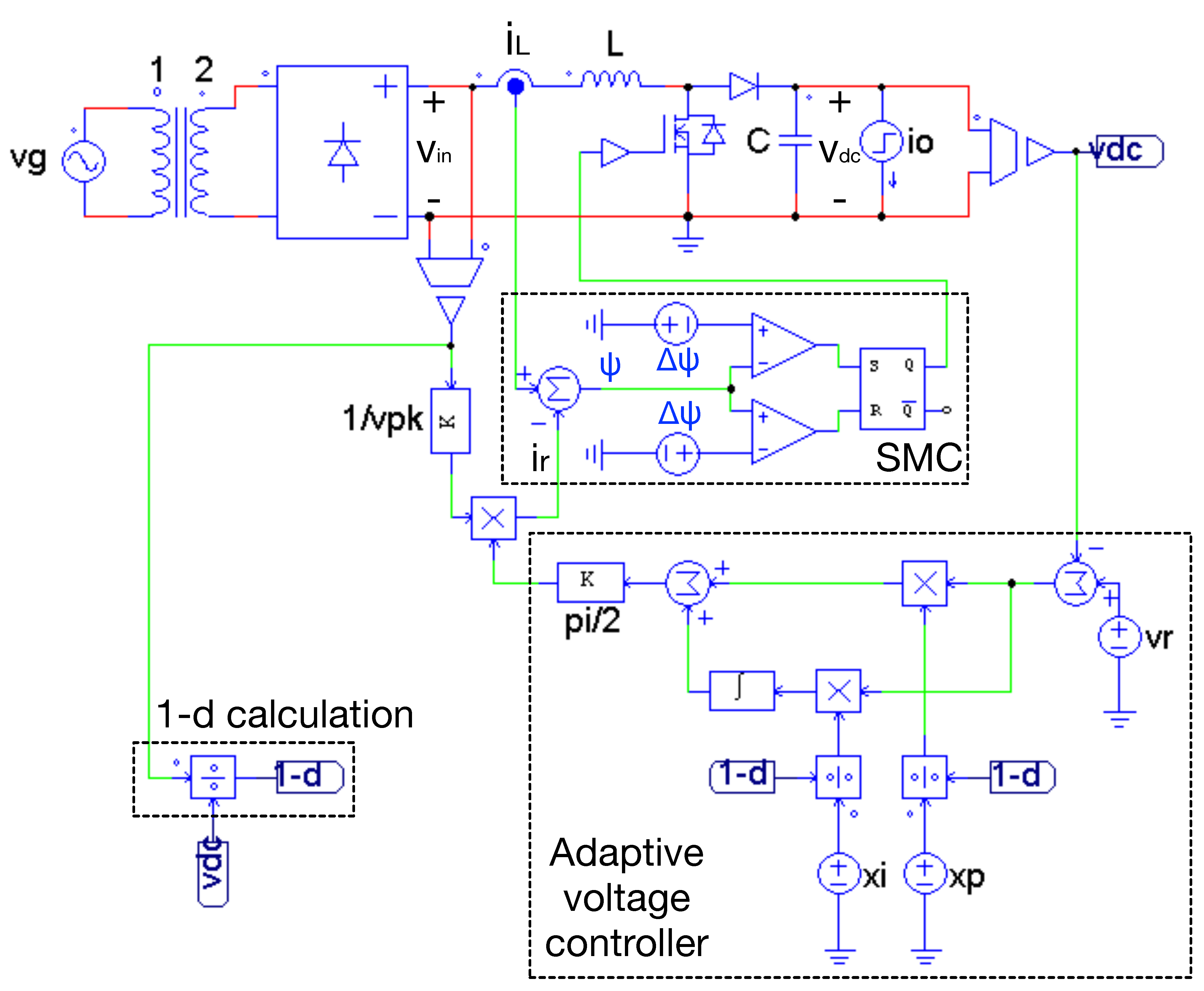
The proposed solution was implemented in the power electronics simulator PSIM, which is an industry standard. Figure 13 depicts the electrical implementation of both the power and control stages, where the control stage is divided into the current SMC and the adaptive voltage controller. Such an scheme is based on power elements (inductor, capacitor, MOSFET, diode, bridge rectifier, transformer), current and voltage sensors, gains, analog comparators, a flip-flop, adders, and analog multipliers and dividers, which are available as integrated circuits. In this way, the SMC can be implemented using a TS555-integrated circuit, where the hysteresis band is defined with a constant gain, as reported in [37]. The adders, subtractors, constant gains, and integrator can be implemented using operational amplifiers, and the constant values can be defined with zener diodes and variable resistors. The multiplications and divisions are commonly implemented using analog circuits such as the HA-2557 [38], RC4200 [39], and AD533 [40]; while the current sensor is usually a small shunt resistor. It is also important to avoid the chattering phenomenon [41], which is caused by a high-frequency switching of the sliding mode controller exiting nonmodeled dynamics of the system. In [41], it was demonstrated that the first step for avoiding this phenomenon is to limit the switching frequency, which was already discussed in Section 2.2.4. Therefore, the final step is to select analog circuitry fast enough to avoid sensible chattering effects on the SMC. For the example designed in the previous section, the switching frequency is limited up to 300 kHz; thus, the analog circuitry for the implementation must have a bandwidth larger than 1.0 MHz, which are not difficult to find.
The simulation of the previous PSIM circuit are presented in Figure 14, where the current requested to the bridge rectifier ( i L ) is equal to the reference ( i r ), which confirms the accuracy of the current SMC. Moreover, the simulation validates the accuracy of the reference generation, since the voltage ( v i n ) and current ( i L ) at the bridge rectifier output are in phase. This is further confirmed by the current ( i g ) and voltage ( v g ) waveforms of the grid, which are in phase. In fact, the simulation data reports a grid-side power factor P F = 0.9997 and a T H D = 1.84 × 10 2 %, which is close to an ideal condition ( P F = 1 , T H D = 0%). Finally, Figure 14 also reports the switching frequency of the MOSFET and diode, which is limited to 300 kHz as expected.
Section 2.3 discussed the possible instability of the rectifier when v i n is near to zero, which is confirmed in the zoom presented in Figure 15. Such a figure confirms that the designed value for L ensures that the switching function Ψ is always inside the hysteresis band, thus the inductor current closely follows the reference. The figure also shows the same waveform around v i n = v p k , where the switching function is always triangular and inside the hysteresis band. Therefore, this simulation confirms the correct operation of the SMC, and the correct design of L and Δ Ψ .
The previous fact is emphasized by changing the inductor value as given in Figure 16: the first simulation at the left is performed with an inductor with half the designed size, which ensures global stability; however, the switching frequency is much higher than the design limit, so it is not suitable for the application example. The simulation at the middle is performed with an inductor of twice the designed size, which ensures a switching frequency lower than the design limit, but near v i n = 0 the switching function operates outside the hysteresis band, which causes a current distortion, thus degrading the power factor and THD. The simulation at the left was performed with a much higher inductor (five times the designed size) to illustrate the problem of over-dimensioning the inductor: the switching function operates much further from the hysteresis band, which causes a larger distortion into the inductor current, which is translated into a distorted grid current; in fact, the simulation shows that in this last case, 11% of the negative semi-cycle of the grid current is distorted, which significantly impact the power factor and THD. Therefore, it is confirmed that not following the proposed design process could produce excessively high switching frequencies or unstable behaviors.
The previous simulations have confirmed the correct operation of the proposed solution at the AC side. Similarly, the simulation reported in Figure 17 shows the waveforms at the DC side. This simulation considers a step change on the load current from 1 A to 2 A, which corresponds to I o = 1 A and I o , m a x = 2 A. The upper waveforms show the load voltage v d c and the corresponding average value v d c , which confirm the expected settling time t s = 100 ms and maximum deviation M O d c = 9.96 V, those in agreement with the maximum limits defined in Table 2. The figure also shows the average value of the peak current i p k , which corresponds to the output of the adaptive voltage controller; moreover, the adaptive parameters of the voltage controller ( k p and k i ) are also depicted in this figure. In conclusion, this simulation confirms the designed dynamic behavior is achieved.
In addition, Figure 18 provides a zoom of the low-frequency ripple at both steady-state conditions ( I o = 1 A and I o = 2 A). Since the design of Δ v d c is performed for I o , m a x = 2 A, the voltage ripple at that condition perfectly march the expected value Δ v d c = 3.2 V, while for I o = 1 A the voltage ripple is much smaller. Therefore, the simulations reported in Figure 17 and Figure 18 confirm the correct operation of the adaptive voltage controller, and the correct design of C.
An additional simulation was performed to evaluate the robustness of the proposed controller to changes on the grid voltage. Moreover, such a simulation also compares the performance of the proposed solution with the control system reported in [21] (named feedforward), which provides a fair comparison since both controllers have adaptive gains calculated to compensate for changes on the operating conditions, and both controllers require the same measurements (inductor current i L , input voltage v i n and dc voltage v d c ). Figure 19 shows the simulation results, where the same Boost-based rectifier is controlled by both solutions. The simulation considers two perturbations: a 50% reduction in the load current i o and a 50% reduction in the magnitude of the grid voltage v g . As expected, the proposed solution is robust to perturbations on both the load current and grid voltage, providing the same performance on the DC voltage v d c for all operating conditions, i.e., without additional overshoots/undershoots. Instead, the feedforward solution introduces an additional undershoot on the DC voltage v d c , f f when the load current is decreased; similarly, it introduces an additional overshoot on v d c , f f when the magnitude of the grid voltage is decreased. Moreover, the voltage deviations on the load provided by the proposed solution are smaller, and the settling-time of the DC voltage is shorter. The fast response of the SMC improves the performance of the proposed solution, where the adaptive voltage loop ensures the same performance for any operating condition. Instead, the calculation of the adaptive gains of the feedforward solution require the data generated by a peak detector, which introduces a delay equal to half of the grid period, thus delaying the compensation of the DC voltage in comparison with the proposed SMC.
The robustness of the proposed controller to variations on the inductor and capacitor values is evaluated in the simulation presented in Figure 20, which considers a load current perturbation of 50 %. In addition, the simulation considers variations on the inductor and capacitor from 95 % to 105 % of the nominal values. The simulation results show that the control system provides the same dynamic response on the DC voltage even with variations on those parameters. Therefore, those results verify the robustness of the proposed controller to variations on the electrical components, which could be caused by aging or manufacturer tolerances.
Finally, the results presented in this section confirm the main contributions of the proposed approach for an application example, illustrating that it can be applied to other Boost-based PFC rectifiers with different power levels, design criteria, load characteristics, and grid voltage parameters. These results show that the proposed design procedure of the Δ Ψ and L guarantees the SMC stability under different disturbances and operating conditions. Moreover, the results also show that the procedure to design C provides the desired maximum overshoot and maximum ripple of v d c . Further, the proposed procedure to dynamically adapt k p and k i of the v d c PI regulator, ensures the desired damping ratio and settling time for any operating condition and disturbances on i d c and v p k .

4. Discussion

A co-design procedure of the control system and power stage of Boost-based PFC rectifiers has been introduced. This procedure assures the system stability in any operating condition, even when the input voltage is close to 0 V. In addition, the design procedure guarantees a maximum converter switching frequency as well as the meet of the desired dynamics of the DC voltage: maximum ripple, desired damping ratio, and settling time and maximum overshoot before load disturbances. In the proposed cascade controller, the outer loop is an adaptive PI regulator of the DC voltage and the inner loop is an SMC to set the inductor current. The paper includes the stability analysis of the SMC as well as a detailed procedure to design the converter inductor, capacitor, and the parameters of the PI regulator to meet the desired performance.
Simulation results of an application example in the specialized software PSIM validate the proposed procedure and show that the system is stable, i.e., Ψ is inside the hysteresis band, in any operating condition. Moreover, the results also show that the DC voltage meets the design requirements, since, on the one hand, it is regulated to the desired reference (220 V) with the desired maximum ripple ( Δ v d c = 4 V), which is obtained for the maximum current load ( I o , m a x = 2 A). On the other hand, the results also show that the controller provides zero steady-state errors before a step in the load with a settling time and maximum overshoot within the desired limits (100 ms and −10 V).
The future work is oriented to the experimental validation of the proposed rectifier and its integration into applications such as electric vehicle chargers or microgrids. In the first case, it requires the design and implementation of a higher-order controller to fulfill the necessities of the batteries’ charging strategy. In the second case, it would require the integration of the proposed rectifier with the microgrid controller through a communication link.

Author Contributions

Conceptualization, C.A.R.-P., A.J.S.-M. and J.D.B.-R.; methodology, C.A.R.-P., A.J.S.-M. and J.D.B.-R.; software, C.A.R.-P., A.J.S.-M. and J.D.B.-R.; validation, C.A.R.-P., A.J.S.-M. and J.D.B.-R.; writing—original draft preparation, C.A.R.-P., A.J.S.-M. and J.D.B.-R.; writing—review and editing, C.A.R.-P., A.J.S.-M. and J.D.B.-R. All authors have read and agreed to the published version of the manuscript.

Funding

This work was supported by the Universidad Nacional de Colombia and the Instituto Tecnológico Metropolitano under the research project “Microinversor de alta eficiencia para maximizar la extracción y transferencia de energía desde paneles fotovoltaicos ubicados en zonas con sombreado parcial a cargas de corriente alterna y voltaje estándar (110 V)” (Hermes code 49938, ITM code PE21103).

Institutional Review Board Statement

Not applicable.

Informed Consent Statement

Not applicable.

Data Availability Statement

The data used in this study are reported in the paper’s figures and tables.

Acknowledgments

The authors thank the Facultad de Minas (Sede Medellin) and Facultad de Ingeniería y Arquitectura (Sede Manizales) of the Universidad Nacional de Colombia.

Conflicts of Interest

The authors declare no conflict of interest.

References

  1. De Castro Pereira, D.; Da Silva, M.R.; Silva, E.M.; Tofoli, F.L. Comprehensive review of high power factor AC-DC boost converters for PFC applications. Int. J. Electron. 2015, 102, 1361–1381. [Google Scholar] [CrossRef]
  2. Ortiz-Castrillón, J.R.; Mejía-Ruíz, G.E.; Muñoz-Galeano, N.; López-Lezama, J.M.; Saldarriaga-Zuluaga, S.D. PFC Single-Phase AC/DC Boost Converters: Bridge, Semi-Bridgeless, and Bridgeless Topologies. Appl. Sci. 2021, 11, 7651. [Google Scholar] [CrossRef]
  3. IEC 61000-3-2:2018; Electromagnetic Compatibility (EMC)—Part 3-2: Limits—Limits for Harmonic Current Emissions (Equipment Input CURRENT ≤16 A Per Phase). IEC: Geneva, Switzerland, 2018.
  4. IEEE. IEEE 519-2014—IEEE Recommended Practice and Requirements for Harmonic Control in Electric Power Systems; IEEE: Piscataway, NJ, USA, 2014. [Google Scholar]
  5. Memon, A.H.; Ali, R.; Memon, Z.A. Discontinuous conduction mode Buck converter with high efficiency. 3C Tecnol. 2021, 10, 35–51. [Google Scholar] [CrossRef]
  6. González-Castaño, C.; Restrepo, C.; Sanz, F.; Chub, A.; Giral, R. DC Voltage Sensorless Predictive Control of a High-Efficiency PFC Single-Phase Rectifier Based on the Versatile Buck-Boost Converter. Sensors 2021, 21, 5107. [Google Scholar] [CrossRef]
  7. Kamalapathi, K.; Priyadarshi, N.; Padmanaban, S.; Holm-Nielsen, J.B.; Azam, F.; Umayal, C.; Ramachandaramurthy, V.K. A Hybrid Moth-Flame Fuzzy Logic Controller Based Integrated Cuk Converter Fed Brushless DC Motor for Power Factor Correction. Electronics 2018, 7, 288. [Google Scholar] [CrossRef] [Green Version]
  8. Umamaheswari, M.G.; Uma, G.; Vijayalakshmi, K.M. Design and implementation of reduced-order sliding mode controller for higher-order power factor correction converters. IET Power Electron. 2011, 4, 984–992. [Google Scholar] [CrossRef]
  9. Yang, J.W.; Do, H.L. Efficient Single-Switch Boost-Dual-Input Flyback PFC Converter With Reduced Switching Loss. IEEE Trans. Ind. Electron. 2015, 62, 7460–7468. [Google Scholar] [CrossRef]
  10. Garcia-Sanchez, J.R.; Hernandez-Marquez, E.; Ramirez-Morales, J.; Marciano-Melchor, M.; Marcelino-Aranda, M.; Taud, H.; Silva-Ortigoza, R. A Robust Differential Flatness-Based Tracking Control for the ‘MIMO DC/DC Boost Converter-Inverter-DC Motor’ System: Experimental Results. IEEE Access 2019, 7, 84497–84505. [Google Scholar] [CrossRef]
  11. Montoya, O.D.; Serra, F.M.; Gil-González, W.; Asensio, E.M.; Bosso, J.E. An IDA-PBC Design with Integral Action for Output Voltage Regulation in an Interleaved Boost Converter for DC Microgrid Applications. Actuators 2022, 11, 5. [Google Scholar] [CrossRef]
  12. Hoyos Velasco, C.I.; Hoyos Velasco, F.E.; Candelo-Becerra, J.E. Nonlinear dynamics and performance analysis of a buck converter with hysteresis control. Computation 2021, 9, 112. [Google Scholar] [CrossRef]
  13. Trujillo, S.C.; Candelo-Becerra, J.E.; Hoyos, F.E. Performance of the boost converter controlled with ZAD to regulate dc signals. Computation 2021, 9, 96. [Google Scholar] [CrossRef]
  14. Wang, Y.; Yang, Y.; Chen, Y.; Pan, T.C.; Guo, C.; Xia, A. Adaptive total sliding mode control for the current of power factor correction circuit. IEICE Electron. Express 2018, 15, 1–12. [Google Scholar] [CrossRef] [Green Version]
  15. Pandey, A.; Kothari, D.P.; Singh, B. Sliding mode control of PFC converter. IETE J. Res. 2005, 51, 371–377. [Google Scholar] [CrossRef]
  16. Kessal, A.; Lazhar, R.; Gaubert, J.P.; Mohammed, M. Analysis and design of an isolated single-phase power factor corrector with a fast regulation. Electr. Power Syst. Res. 2011, 81, 1825–1831. [Google Scholar] [CrossRef]
  17. Genc, N.; Iskender, I. DSP-based current sharing of average current controlled two-cell interleaved boost power factor correction converter. IET Power Electron. 2011, 4, 1015–1022. [Google Scholar] [CrossRef]
  18. Bosque-Moncusi, J.M.; Valderrama-Blavi, H.; Flores-Bahamonde, F.; Vidal-Idiarte, E.; Martínez-Salamero, L. Using low-cost microcontrollers to implement variable hysteresis-width comparators for switching power converters. IET Power Electron. 2018, 11, 787–795. [Google Scholar] [CrossRef]
  19. Chiang, H.C.; Lin, F.J.; Chang, J.K.; Chen, K.F.; Chen, Y.L.; Liu, K.C. Control method for improving the response of single-phase continuous conduction mode boost power factor correction converter. IET Power Electron. 2016, 9, 1792–1800. [Google Scholar] [CrossRef]
  20. Marcos-Pastor, A.; Vidal-Idiarte, E.; Cid-Pastor, A.; Martinez-Salamero, L. Interleaved Digital Power Factor Correction Based on the Sliding-Mode Approach. IEEE Trans. Power Electron. 2016, 31, 4641–4653. [Google Scholar] [CrossRef]
  21. Wu, S.T.; Chen, F.Y.; Chien, M.C.; Wang, J.M.; Su, Y.Y. A Hybrid Control Scheme with Fast Transient and Low Harmonic for Boost PFC Converter. Electronics 2021, 10, 1848. [Google Scholar] [CrossRef]
  22. Kessal, A.; Rahmani, L. Ga-optimized parameters of sliding-mode controller based on both output voltage and input current with an application in the PFC of AC/DC converters. IEEE Trans. Power Electron. 2014, 29, 3159–3165. [Google Scholar] [CrossRef]
  23. Zhou, Y.; Wang, B.L. PWM-quasi-sliding mode control for APFC converters. Electr. Eng. 2010, 92, 43–48. [Google Scholar] [CrossRef]
  24. Karabacak, M.; Poyraz, G. Robust adaptive control of pulse-width modulated rectifiers based on adaptive super-twisting sliding-mode and state feedback controllers. Electr. Power Compon. Syst. 2015, 43, 1289–1296. [Google Scholar] [CrossRef]
  25. Mohanty, P.R.; Panda, A.K. Fixed-Frequency Sliding-Mode Control Scheme Based on Current Control Manifold for Improved Dynamic Performance of Boost PFC Converter. IEEE J. Emerg. Sel. Top. Power Electron. 2017, 5, 576–586. [Google Scholar] [CrossRef]
  26. Kayisli, K.; Tuncer, S.; Poyraz, M. A Novel Power Factor Correction System Based on Sliding Mode Fuzzy Control. Electr. Power Compon. Syst. 2017, 45, 430–441. [Google Scholar] [CrossRef]
  27. Seleme, S.I.; Rosa, A.H.; Morais, L.M.; Donoso-Garcia, P.F.; Cortizo, P.C. Evaluation of adaptive passivity-based controller for power factor correction using a boost converter. IET Control. Theory Appl. 2012, 6, 2168–2178. [Google Scholar] [CrossRef]
  28. Karami, Z.; Shafiee, Q.; Khayat, Y.; Yaribeygi, M.; Dragicevic, T.; Bevrani, H. Decentralized Model Predictive Control of DC Microgrids with Constant Power Load. IEEE J. Emerg. Sel. Top. Power Electron. 2021, 9, 451–460. [Google Scholar] [CrossRef]
  29. Rasoolzadeh, A.; Salmasi, F.R. Reduced-order dynamic model for droop-controlled inverter/converter-based low-voltage hybrid AC/DC microgrids - part 2: DC sub-microgrid and power exchange. IET Smart Grid 2018, 1, 134–142. [Google Scholar] [CrossRef]
  30. Chatrenour, N.; Razmi, H.; Doagou-Mojarrad, H. Improved double integral sliding mode MPPT controller based parameter estimation for a stand-alone photovoltaic system. Energy Convers. Manag. 2017, 139, 97–109. [Google Scholar] [CrossRef]
  31. Taheri, B.; Sedaghat, M.; Bagherpour, M.A.; Farhadi, P. A New Controller for DC-DC Converters Based on Sliding Mode Control Techniques. J. Control. Autom. Electr. Syst. 2019, 30, 63–74. [Google Scholar] [CrossRef]
  32. Sira-Ramirez, H. Sliding Motions in Bilinear Switched Networks. IEEE Trans. Circuits Syst. 1987, 34, 919–933. [Google Scholar] [CrossRef]
  33. Sira-Ramirez, H. Nonlinear variable structure systems in sliding mode: The general case. IEEE Trans. Autom. Control. 1989, 34, 1186–1188. [Google Scholar] [CrossRef]
  34. Villegas Ceballos, J.P.; Serna-Garcés, S.I.; González Montoya, D.; Ramos-Paja, C.A.; Bastidas-Rodríguez, J.D. Charger/discharger DC/DC converter with interleaved configuration for DC-bus regulation and battery protection. Energy Sci. Eng. 2019, 8, 530–543. [Google Scholar] [CrossRef] [Green Version]
  35. Henao-Bravo, E.E.; Saavedra-Montes, A.J.; Ramos-Paja, C.A.; Bastidas-Rodriguez, J.D.; Gonzalez Montoya, D. Charging/discharging system based on zeta/sepic converter and a sliding mode controller for dc bus voltage regulation. IET Power Electron. 2020, 13, 1515–1527. [Google Scholar] [CrossRef]
  36. Umamaheswari, M.G.; Uma, G.; Vijayalakshmi, K.M. Analysis and design of reduced-order sliding-mode controller for three-phase power factor correction using Cuk rectifiers. IET Power Electron. 2013, 6, 935–945. [Google Scholar] [CrossRef]
  37. Gonzalez Montoya, D.; Ramos-Paja, C.; Giral, R. Improved design of sliding mode controllers based on the requirements of MPPT techniques. IEEE Trans. Power Electron. 2016, 31, 235–247. [Google Scholar] [CrossRef] [Green Version]
  38. Intersil. HA-2557 130 MHz, Four Quadrant, Current Output Analog Multiplier. 2002. Available online: https://www.alldatasheet.com/datasheet-pdf/pdf/122864/INTERSIL/HA-2557.html (accessed on 30 March 2022).
  39. Fairchild Semiconductor. RC4200 Analog Multiplier. 2001. Available online: https://www.alldatasheet.com/datasheet-pdf/pdf/54398/FAIRCHILD/RC4200.html (accessed on 30 March 2022).
  40. Analog Devices. AD533 Low Cost IC Multiplier, Divider, Squarer, Square Rooter. 2022. Available online: https://www.analog.com/en/products/ad533.html (accessed on 30 March 2022).
  41. Alsmadi, Y.M.; Utkin, V.; Haj-ahmed, M.A.; Xu, L. Sliding mode control of power converters: DC/DC converters. Int. J. Control. 2018, 91, 2472–2493. [Google Scholar] [CrossRef]
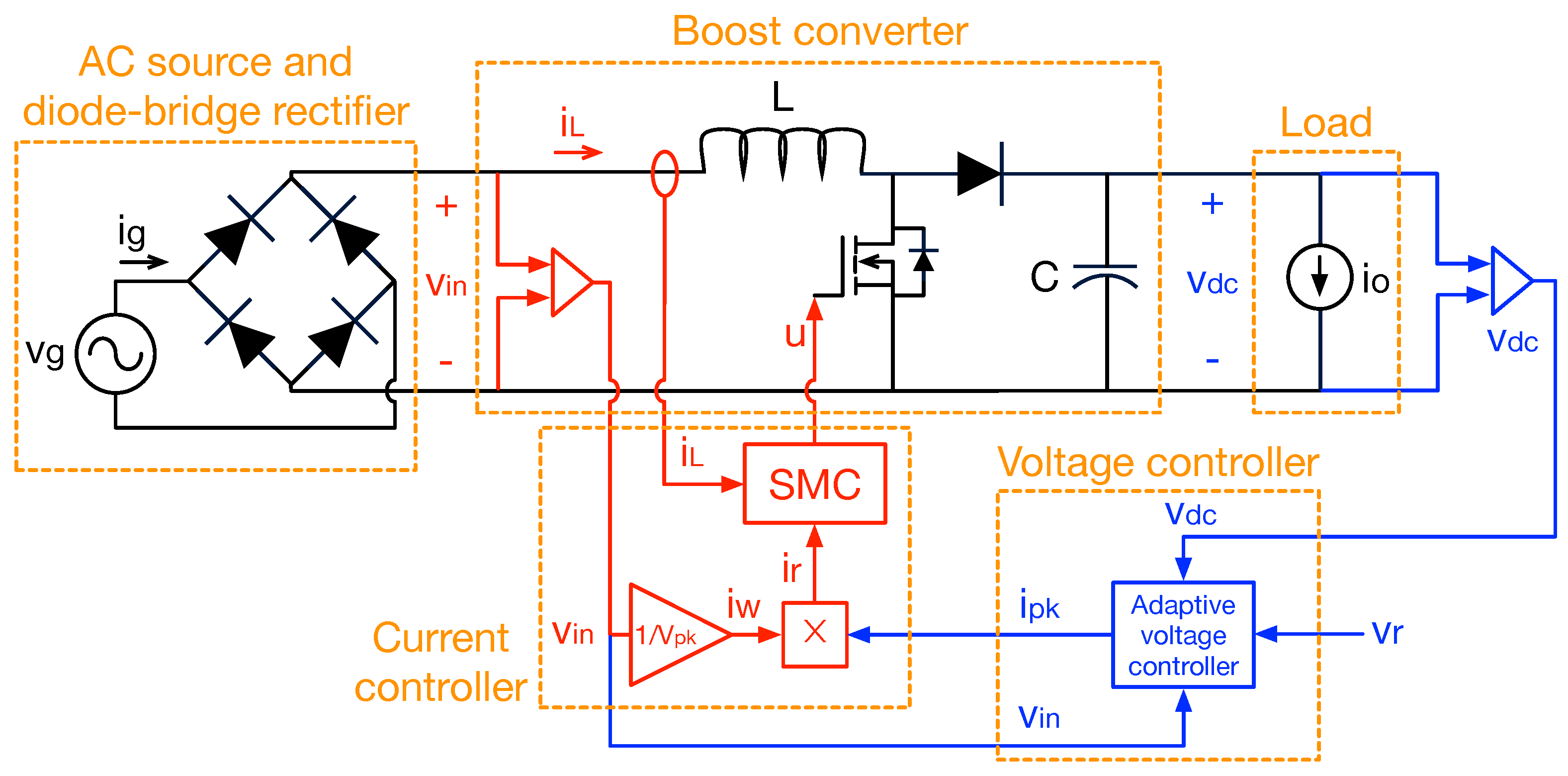
Figure 1. Electrical scheme of the Boost-based rectifier with power factor correction.
Computation 10 00061 g001
Figure 2. Ψ waveform for different values of Δ Ψ and L.
Computation 10 00061 g002
Figure 3. Circuital implementation of the SMC.
Computation 10 00061 g003
Figure 4. Detailed waveform of Ψ when v i n 0 for different L values.
Computation 10 00061 g004
Figure 5. Voltage control loop.
Computation 10 00061 g005
Figure 6. Structure of the adaptive voltage controller.
Computation 10 00061 g006
Figure 7. Output port model for analyzing the low-frequency voltage ripple at the DC side.
Computation 10 00061 g007
Figure 8. Low-frequency ripple waveforms at the DC side.
Computation 10 00061 g008
Figure 9. Scheme of the application example.
Computation 10 00061 g009
Figure 10. Design of the inductor L and hysteresis band Δ Ψ .
Computation 10 00061 g010
Figure 11. Design of the capacitor C.
Computation 10 00061 g011
Figure 12. Flowchart of the design process.
Computation 10 00061 g012
Figure 13. Application example implemented in the power electronics simulator PSIM.
Computation 10 00061 g013
Figure 14. Validation of the SMC, inductor current and hysteresis band.
Computation 10 00061 g014
Figure 15. Zoom at v i n around 0 V (left) and v i n around v p k (right).
Computation 10 00061 g015
Figure 16. Effects of violating the L and Δ Ψ design.
Computation 10 00061 g016
Figure 17. Validation of the capacitor and adaptive controller.
Computation 10 00061 g017
Figure 18. Validation of the low-frequency ripple.
Computation 10 00061 g018
Figure 19. Performance comparison of the proposed solution with a feedforward/feedback controller.
Computation 10 00061 g019
Figure 20. Evaluation of the controller robustness to variations on the inductor and capacitor.
Computation 10 00061 g020
Table 1. PFC main perturbations, causes and effects.
PerturbationMain CauseMain Effect
Change in i d c Connection/disconnection of loadsReduction/increment in v d c
Change in v p k Sag/swell in grid voltageReduction/increment in v d c
Table 2. Parameters for the application example.
ParameterValueParameterValue
v p k 84.85 V v d c 220 V
f g 60 Hz F s w , m a x 300 kHz
I o 1 A I o , m a x 2 A
M O d c −10 V Δ v d c 4 V
ρ 0.707 t s , 2 % 100 ms
Publisher’s Note: MDPI stays neutral with regard to jurisdictional claims in published maps and institutional affiliations.