Article

Four-Switch Three-Phase PMSM Converter with Output Voltage Balance and DC-Link Voltage Offset Suppression

1
National School of Applied Sciences, Mohammed First University, Oujda BP 669, 60000, Morocco
2
National School of Applied Sciences, Cadi Ayyad University, Marrakech BP 575, 40000, Morocco
*
Author to whom correspondence should be addressed.
Information 2017, 8(1), 11; https://doi.org/10.3390/info8010011
Submission received: 15 October 2016 / Revised: 9 January 2017 / Accepted: 12 January 2017 / Published: 17 January 2017

Abstract

:
High power quality, efficiency, complexity, size, cost effectiveness and switching losses of the direct current to alternating current (DC–AC) conversion system are crucial aspects in industrial applications. Therefore, the four-switch three-phase inverter (4S3P) has been proposed as an innovative inverter design. However, this topology has been known to have many performance limitations in the low-frequency region, because of the generation of an unbalanced voltage leading to an unbalanced current due to the fluctuation and offset of the centre tap voltage of the DC-link capacitors. Those drawbacks are investigated and solved in this paper in order to provide pure sinusoidal output voltages. The generated output voltages are controlled using proportional-integral (PI) controllers to follow the desired voltages. Furthermore, the DC-link capacitor voltage offset is mitigated by subtracting the direct component from the control reference voltage using low pass filters, where this direct voltage component provides the direct current component which leads to DC-link capacitor voltage divergence. A simulation model and experimental setup are used to validate the proposed concept. Many simulation and experimental results are carried out to show the effectiveness of the proposed control scheme.

1. Introduction

The 4S3P inverter is a low-cost attractive power topology that has attracted the interest of many researches in the last decades. It was first proposed by [1] for the purpose of minimizing the components’ cost; one motor terminal is connected to the centre tap of the DC-link capacitors so that it utilizes two less Insulated Gate Bipolar Transistors (IGBT) [2]. This converter was applied to many fields such as Brushless direct-current (BLDC) motor drives [3,4] and unified power quality conditioners [5]. In addition, the 4S3P power topology could be achieved from standard three-phase topology, which made it very attractive in fault-tolerant control to solve the open/short circuit fault of standard inverter IGBTs [6,7]. The 4S3P inverter conception applied to the fault-tolerant control is very valuable in some critical applications such as wind energy conversion systems [8] and alternating current (AC) motor drives [9].
However, the cost reduction ensured by 4S3P inverters is at the expense of output performance, and they are known to have numerous limitations and drawbacks compared to the 6S3P inverter; the voltage utilization factor is halved compared to the six-switch inverter. On the other hand, the capacitor centre tap voltage is fluctuating and presents an offset which destroys the balance among the motor phase currents [10]. That voltage fluctuation and offset are caused by the third load current alternative and direct component which flow through capacitors that are exploited to create a fixed power supply mid-point. As a result, voltage fluctuations as well as current unbalance are increased as the load torque becomes higher or the frequency becomes lower. This current and voltage unbalance could lead to inverter failure, torque pulsation, and system break down [11].
In order to overcome those shortcomings, much research has been done, as shown in the literature. In [11], a motor current unbalance is investigated and a current distortion compensation scheme is proposed. Authors in [12] proposed a compensation method by adjusting switching times, considering the capacitor centre tap voltage fluctuation. In [13] the cause and effect of the capacitor centre tap voltage fluctuation in an analytical point of view was investigated, and the capacitor voltage offset was suppressed by employing certain switching states. However, the capacitor voltage offset suppression was achieved at the cost of the inverter output performance.
In this paper, the main reasons invoking motor current unbalance and torque pulsation as well as DC-link capacitors voltage offset are investigated. A voltage control method that utilizes 4S3P inverter output voltage feedback is proposed and associated to low pass filters to eliminate capacitors’ voltage offset. This paper is organized as follows: in Section 2, a general model of the four-switch inverter is illustrated and non-ideal behaviours of the four-switch inverter are discussed; then, its impact on the PMSM behaviour is revealed. The voltage balance and the offset suppression are shown in Section 3. Section 4 shows the simulation results of both the traditional and proposed balancing schemes, and corroborates the expected features of the proposed method through experimental results. Finally, some conclusions are presented.

2. Four-Switch Three-Phase Inverter for PMSM Drives

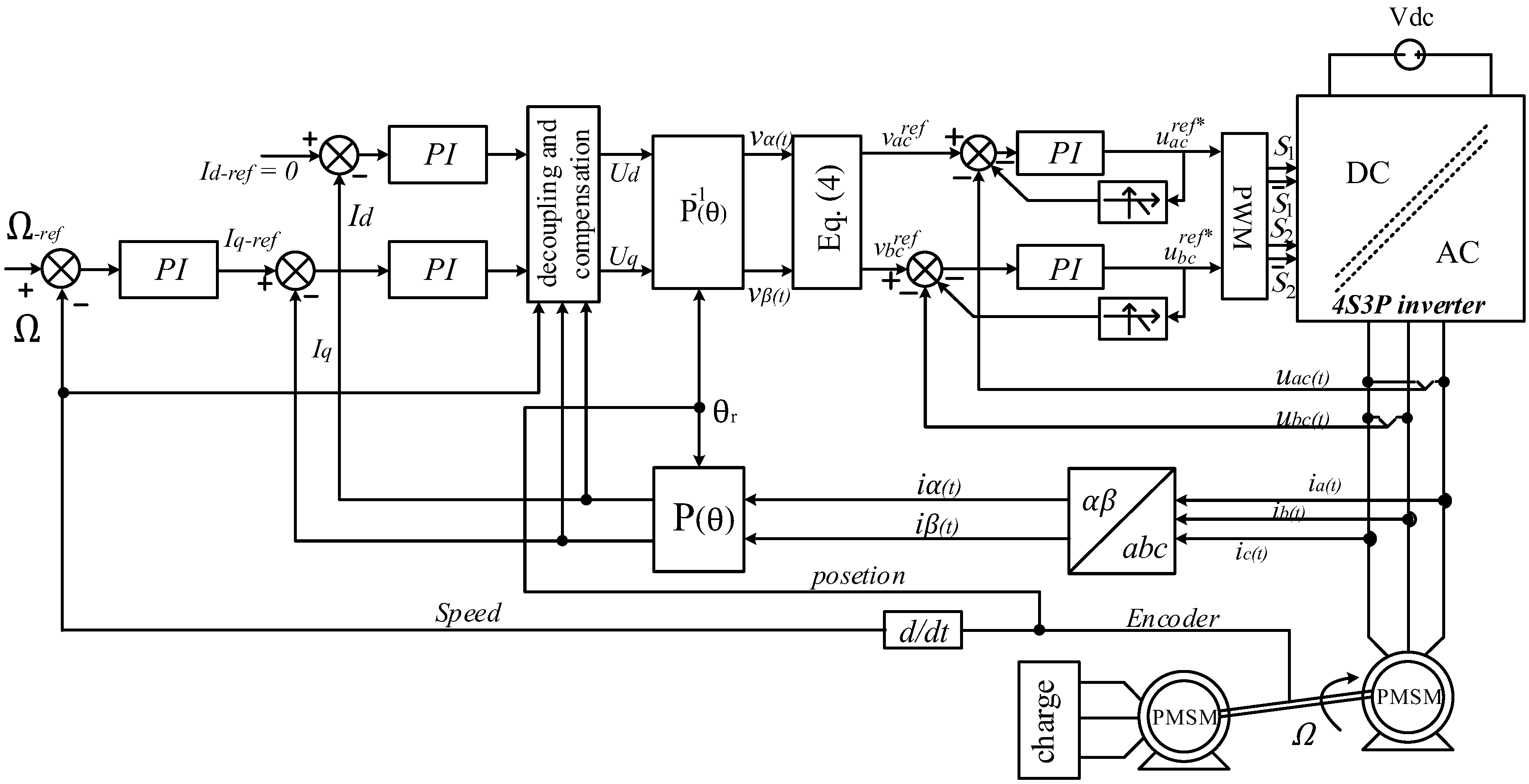
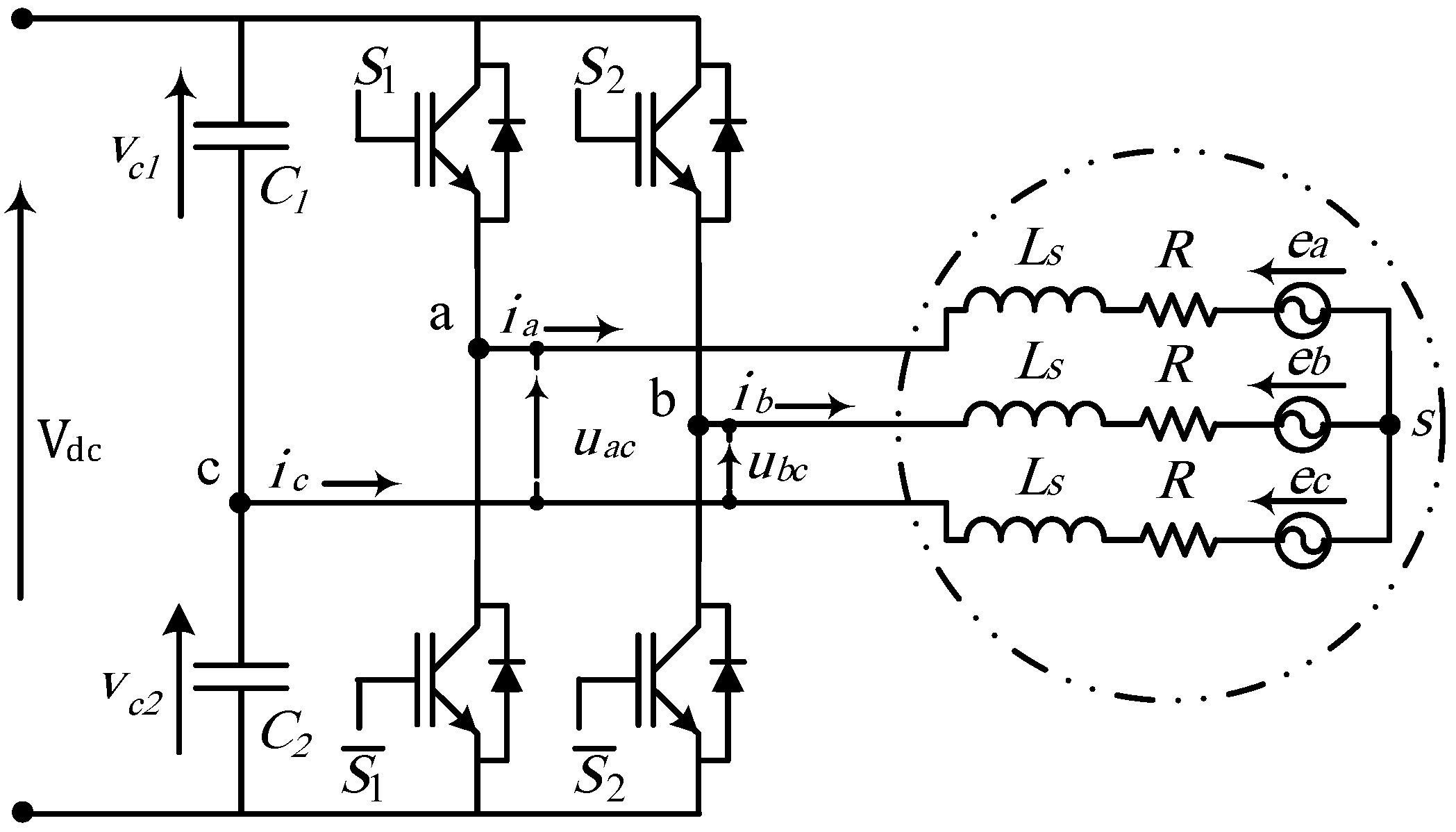
2.1. 4S3P Inverter Configuration and Operation

The 4S3P inverter is one of the solutions used for the inverter one-leg fault-tolerant control while transistor open/short circuit; the faulty leg is separated and the associated phase is connected to the capacitor midpoint. This strategy is of interest to the authors of [3,4,5,6,7,8,9,10,11]. The final power inverter structure is shown in Figure 1. The 4S3P inverter includes four groups of IGBT and anti-paralleled diodes, as well as two capacitors. The switches’ and capacitors’ mid-points are connected in parallel to the PMSM. In addition, the power topology presented in Figure 1 can be considered as a cost-reduction solution with only four switches. The low component cost is required in many applications; however, that will alter the output performance.
In Figure 1, the 4S3P inverter line-to-line output voltages are denoted by uac and ubc. The vas, vbs and vcs are the line-to-neutral output voltage. The capacities of C1 and C2 are equal to C, and their voltages are denoted by Vc1 and Vc2 respectively. The direct current (DC) bus voltage is denoted by Vdc. Moreover, the switches’ states can be denoted by Boolean variables s 1 , s ¯ 1 , s 2 , s ¯ 2 . Therefore, the binary value “1” of each switch will indicate the closed state, and the binary value “0” will indicate the opened state. As a result, the generated voltage can be depicted as follows.
u a c = V d c 2 ( 2 s 1 ) v c 2 u b c = V d c 2 ( 2 s 2 ) v c 2 u a b = V d c 2 ( 2 s 1 1 ) V d c 2 ( 2 s 2 1 )
The DC-link capacitor voltages can be decomposed as a fluctuating voltage and a direct voltage ( v c 1 = V d c / 2 v c , v c 2 = V d c / 2 + v c ). In addition, and from [11], the voltage fluctuation is depicted as follows.
v c = 1 / 2 C i c ( t ) dt
The fluctuating voltage amplitude depends on the DC-link capacitor value, the ic currant amplitude, and the PMSM speed. Using the average method, the average output voltage can be written as.
u a c = v a r e f + v c u b c = v b r e f + v c u a b = v a r e f v b r e f
where v a r e f and v b r e f are respectively the a and b leg reference voltage modulated using PWM, and the obtained pulsations are given to the related leg transistors; pulsations are obtained from the v a r e f modulation control s 1 and s ¯ 1 , while pulsations are obtained from the v b r e f modulation control s 2 and s ¯ 2 .
To generate a balanced voltage by the 4S3P inverter, according to the standard control strategy [11], the reference voltages presented in Equation (4) must be applied.
v a r e f = 3 V m cos ( θ r π / 6 φ ) v b r e f = 3 V m cos ( θ r π / 2 φ )
where θ r is the PMSM electrical rotor position, V m and φ are respectively the reference voltage amplitude and phase; they are used to control direct and quadratic PMSM currents as is described in [14]. As a result, from Equation (3), the relation between the line-to-neutral voltages vas, vbs and vcs, and the reference voltages ( v a r e f , v b r e f ), can be computed as is shown in Equation (5)
v a s = ( 2 v a r e f v b r e f v c ) / 3 v b s = ( 2 v b r e f v a r e f v c ) / 3 v c s = ( v a r e f v b r e f + 2 v c ) / 3
Equation (5) can be schematized in the rotating reference frame as is shown in Figure 2. The ideal inverter behavior where capacitors’ fluctuating voltage is neglected is presented in the left one, and the real case where the presence of capacitors’ fluctuating voltage leads to the generation of unbalanced voltages is presented in the right one.
As is exposed in Equation (2), the Vc depends on the PMSM rotor position, as a result, the line-to-neutral generated voltages include an instantaneous voltage ripple, which leads to PMSM current and torque pulsation as well as motor vibration.

2.2. PMSM Modelling and Current Ripple Determination

Generally, PMSM speed control, rotor position estimation and control at fault detection require a machine model with an average complexity level. Indeed, controllers exploited to achieve the motor speed and current monitoring, tolerate several modelling simplifications and uncertainty, such as the perfect sinusoidal distribution of stator winding. In addition, the produced magneto-motive-forces and the magnitude flux linkage through the stator winding can be assumed sinusoidal. The electrical dynamics of a permanent magnet synchronous motor in the synchronously rotating reference frame (abc axis) can be expressed by [13,14,15].
v a s ( t ) = R i a ( t ) + d ψ a ( t ) / dt v b s ( t ) = R i b ( t ) + d ψ b ( t ) / dt v c s ( t ) = R i c ( t ) + d ψ c ( t ) / dt
where R is the rotor resistance, i a , b , c ( t ) are the stator currents and ψ a , b , c ( t ) are the stator flux.
However, the flux ψ a , b , c ( t ) is a result of stator windings and rotor permanent magnet flux. They can be presented in the rotating reference frame linked to the stator as:
[ ψ a , b , c ( t ) ] = [ L M M M L M M M L ] [ i a , b , c ( t ) ] + Ψ m [ cos ( θ r ) cos ( θ r 2 π / 3 ) cos ( θ r + 2 π / 3 ) ]
where L and M are respectively, the self-inductance of the stator winding and the mutual-inductance between the windings. Ψm is the maximal amplitude of the permanent magnet flux, and θr is the electrical rotor position.
As the synchronous motor investigated in this paper is a surface mounted permanent magnet motor, the quantities L and M are constants. Consequently, the notation Ls = LM can be made to simplify modelling Equation (8).
As one can observe from Equation (5), the generated voltages are a combination of the involved voltage v a s , b s , c s r e f , and the other voltage component caused by DC-link capacitor voltage fluctuation which can be depicted by v c in Equation (8) [16,17]. So, the PMSM final model, in stationary reference frame considering voltage fluctuation, can appear as:
v a s r e f v c = R i a + L s d i a / d t + e a R i c L s d i c / dt v b s r e f v c = R i b + L s d i b / dt + e b R i c L s d i c / dt v c s r e f + 2 v c = R i c + L s d i c / dt + e c wanted   behavior + 2 R i c + 2 L s d i c / dt current   ripple  where  v a s r e f = 2 v a r e f v b r e f 3 v b s r e f = 2 v b r e f v a r e f 3 v c s r e f = v a r e f v b r e f 3  and  v c = v c 3
where i c is the current ripple caused by the capacitor fluctuating voltages. This current has the same PMSM rotor electric pulsation, which leads to rotor vibration and torque pulsation.
T e m = i i e e wanted   Torque + 3 i c e c Torque   ripple
The torque ripple shown in Equation (9) is a product of i c and e c which have the same pulsation. As a result, this torque ripple 3 i c e c manifests as an alternative component with a frequency of 2 d θ r d t = 2 ω in the actual torque.

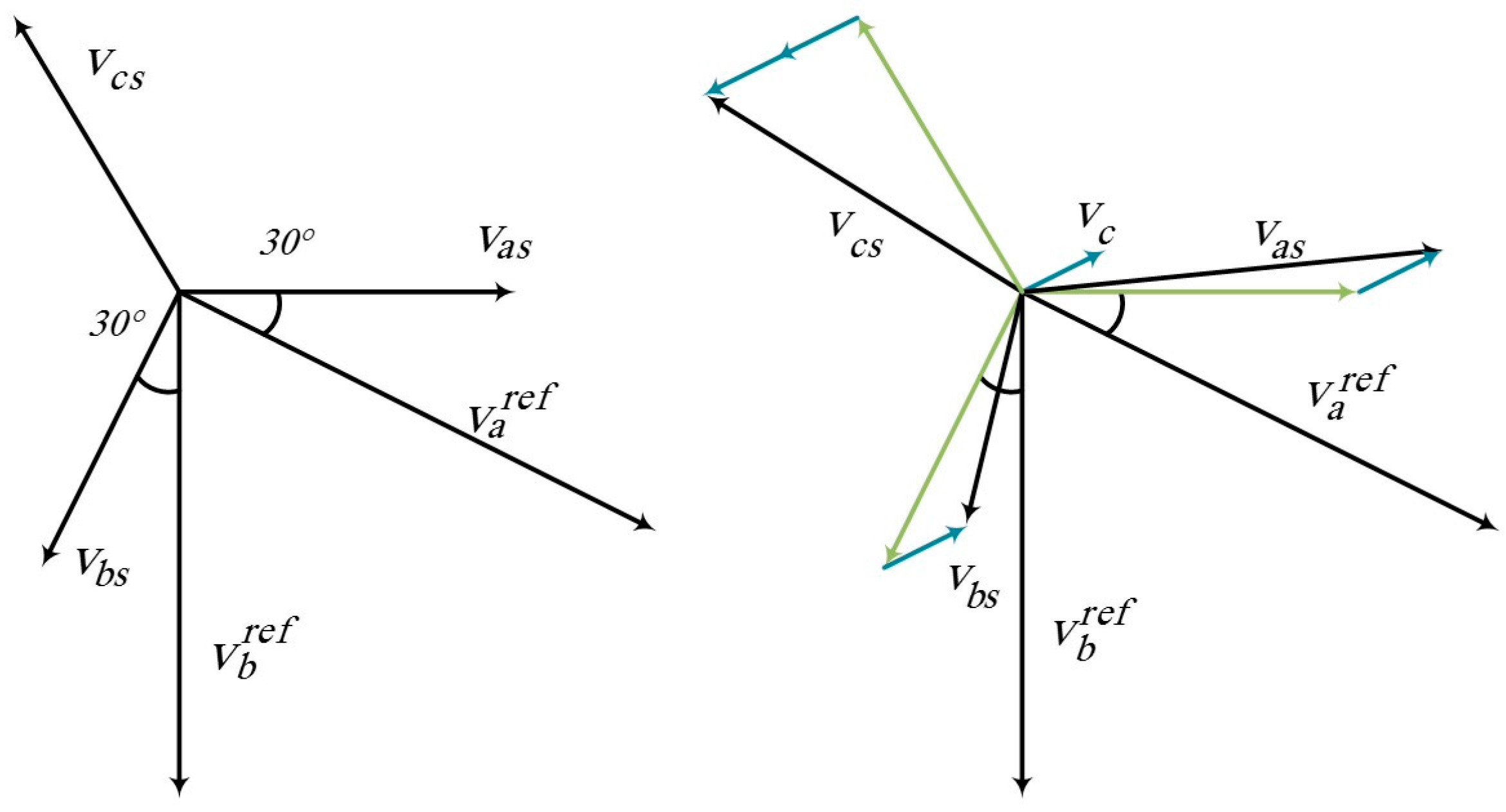
3. Four-Switch Three-Phase Inverter Voltage Balance

By assuming that the used switches are ideal [18,19], and the power and voltage losses are neglected, consequently, the PMSM behavior can be modelled as in Equation (8), due to the DC-link fluctuating voltage which affects the generated voltage as is clearly seen in Equation (3). To mitigate this voltage fluctuation v c as well as the current ripple component i c , two PI controllers are added to control the generated voltages u a c , u b c to be equal to the reference voltages v a c r e f , v b c r e f . In the ideal case, the output of controllers is as follows.
u a c r e f = P I ( v a c r e f u a c ) u b c r e f = P I ( v b c r e f u b c )
where (PI) denoted in the time-domain by K P ( . ) + K I ( . ) is a PI controller, where Kp and KI are the proportional and integral gains, respectively. However, the newest generated voltage references can be affected by sensors’ offset at speed transient states. As a result, a supplementary DC component can appear at the inverter output, and it can be intensified by the integral gains at references.
Therefore, the DC-link capacitor voltage becomes imbalanced. To overcome that effect, low pass filters are added, and their outputs are subtracted from the reference voltages. As a result, only AC reference components are sent to the PWM module, and generated by the 4S3P inverter. The response time is chosen in order to ensure good performance, and the open loop transfer function is depicted in Equation (11).
H O = s K P + K I s ( 1 + τ s )
where s is the derivative operator, and τ is the low pass filter response time, it equates to τ = 0.25 s , taken as an optimal value. If a small value was used, the sinusoidal component at a low range of speed would not be filtered. However, if a large one is utilized, the offset suppression would become slow. The presented method’s effectiveness is validated by simulation and experimentally in the following section.

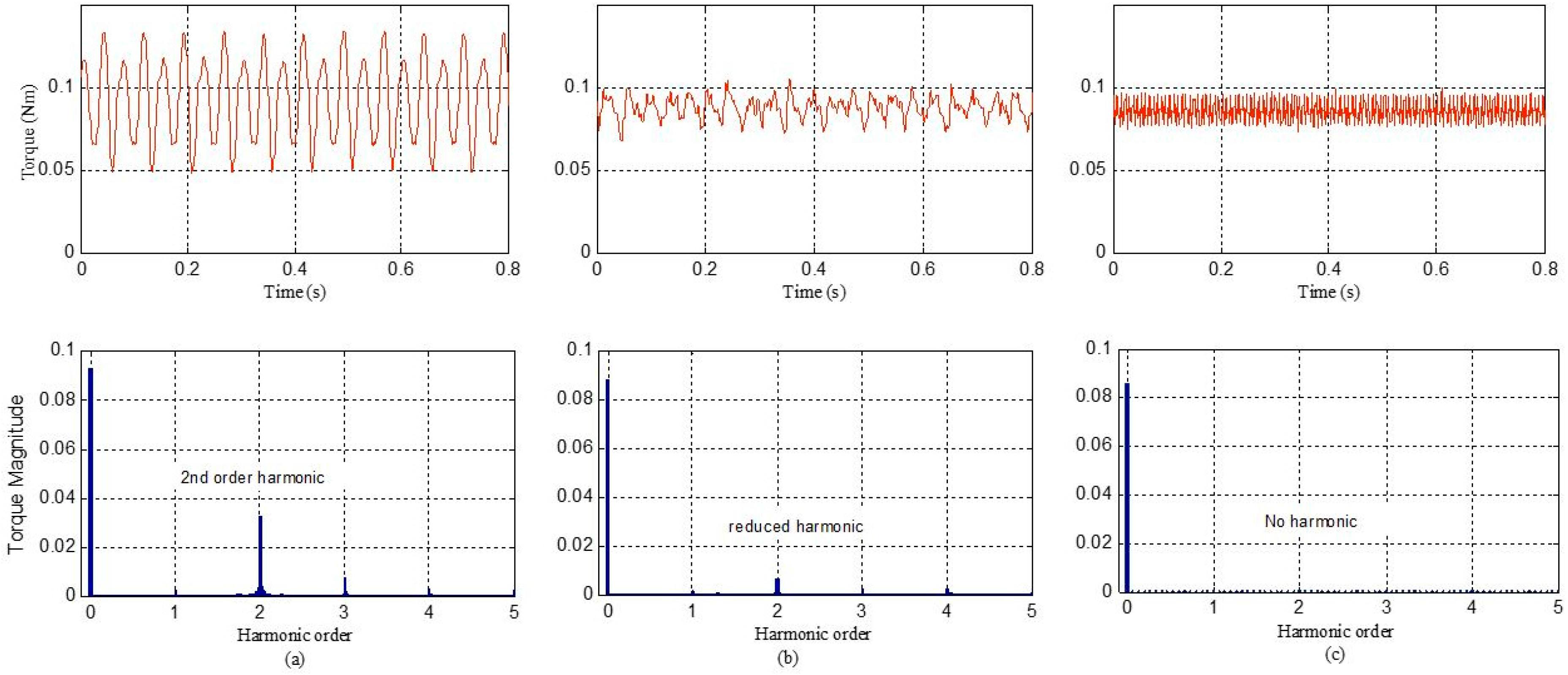
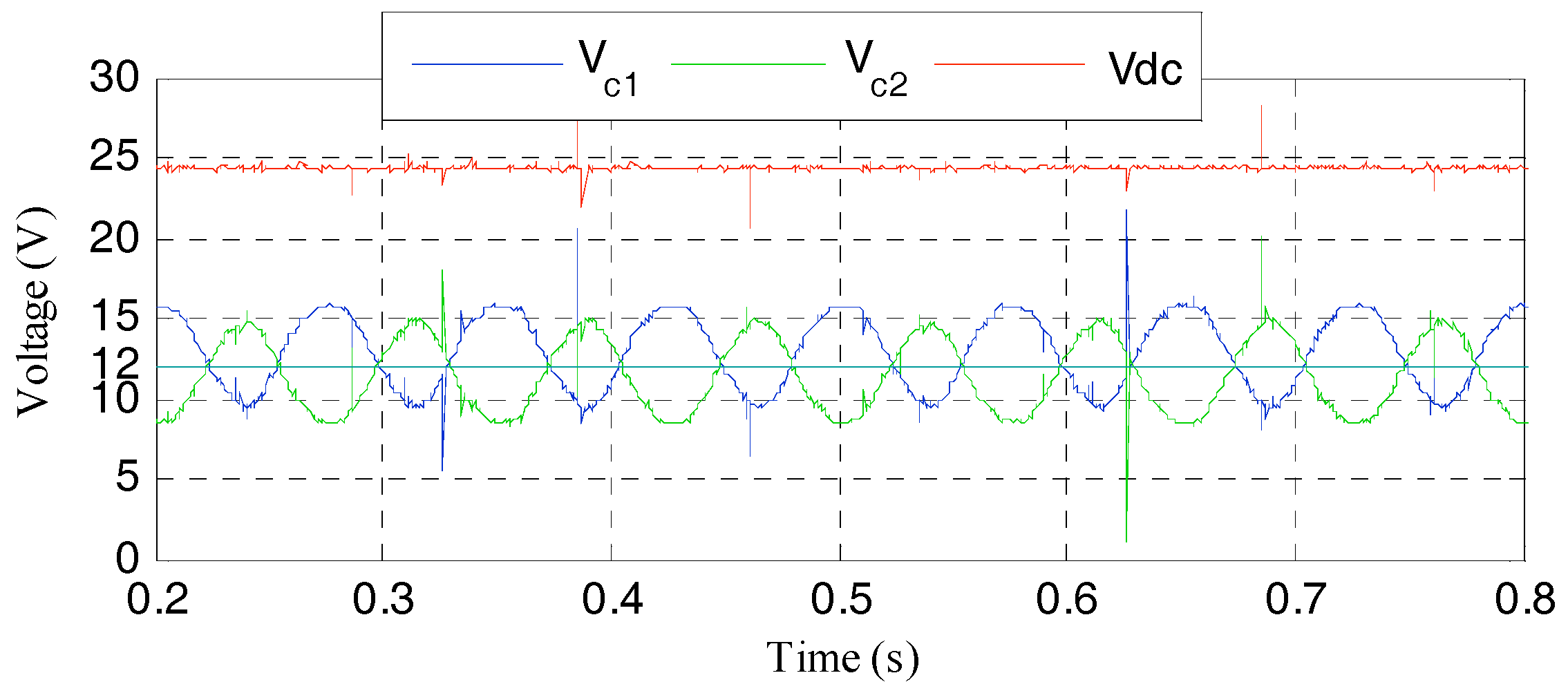
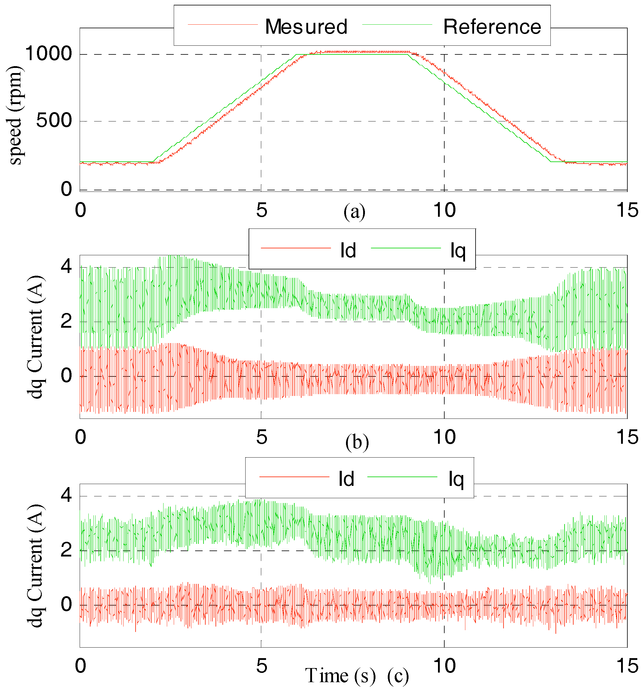
4. Simulation and Experimental Results

The proposed scheme [13], presented in Figure 3, and the power configuration were tested in simulation; the power structure was assembled in PSIM which had been interconnected to Matlab/Simulink. In addition, the control scheme and the proposed voltage balance were built in Simulink. The validated algorithm was then implemented by means of the test bench shown in Figure 4.
The drive system is controlled by a 32-bit fixed-point TMS320-F28335 DSP board, based on a 150 MHz clock; it has been programed using rapid prototyping tools of Matlab/Simulink®. A Matlab/GUI real-time interface locally built was used to make results easy to record [14]. The power structure includes a four-switch three-phase inverter associated to split capacitors. The 4S3P inverter is feeding a PMSM with Surface Magnet Mounted. Parameters and other configuration requirements are presented in Table 1 and Table 2. To operate around the nominal point, the PMSM was loaded by a DC generator supplied by a current source to establish a fixed load torque. An incremental encoder was used to measure the rotor position (2000 pulses per revolution). This equipment is illustrated in Figure 4.

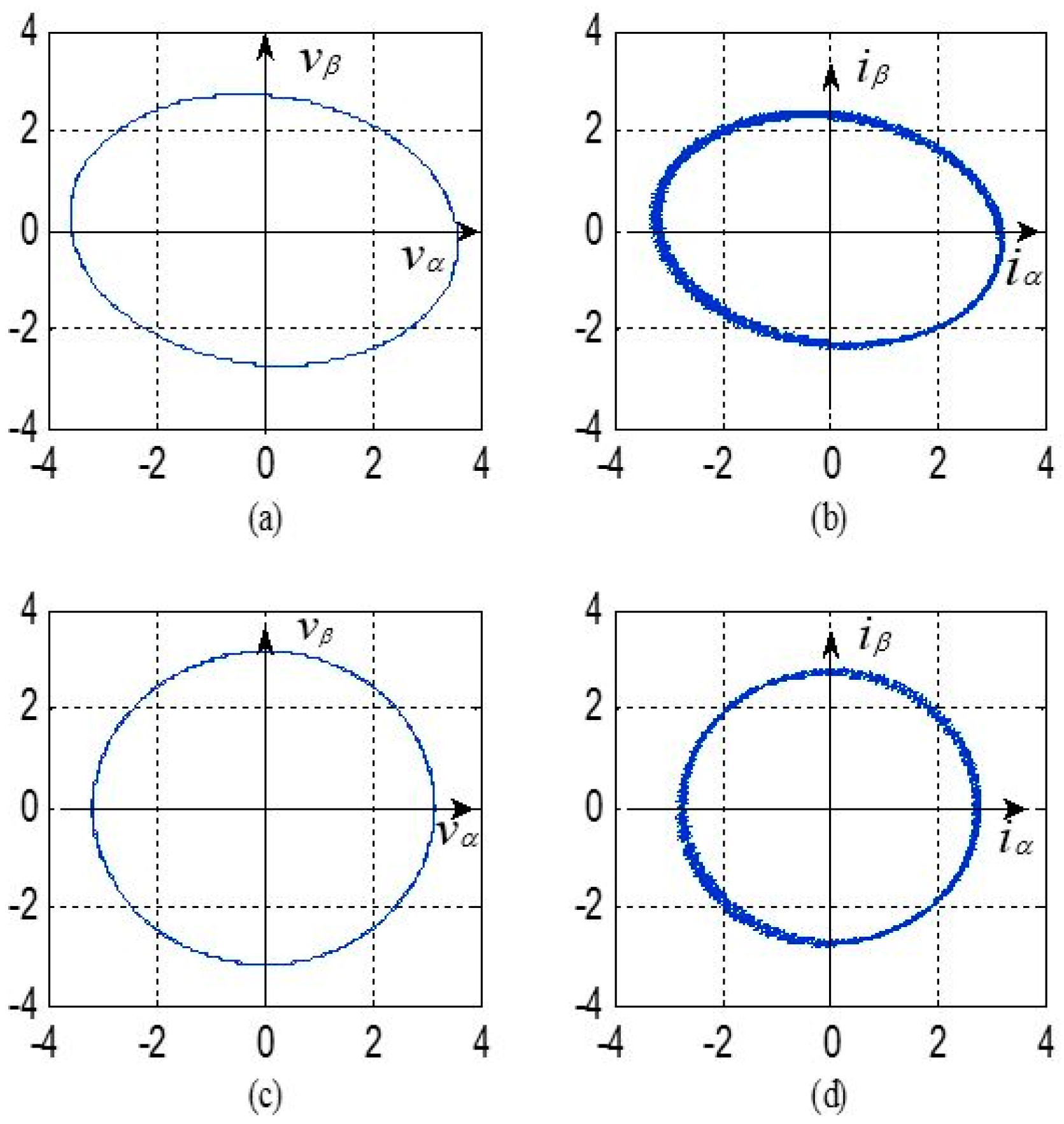
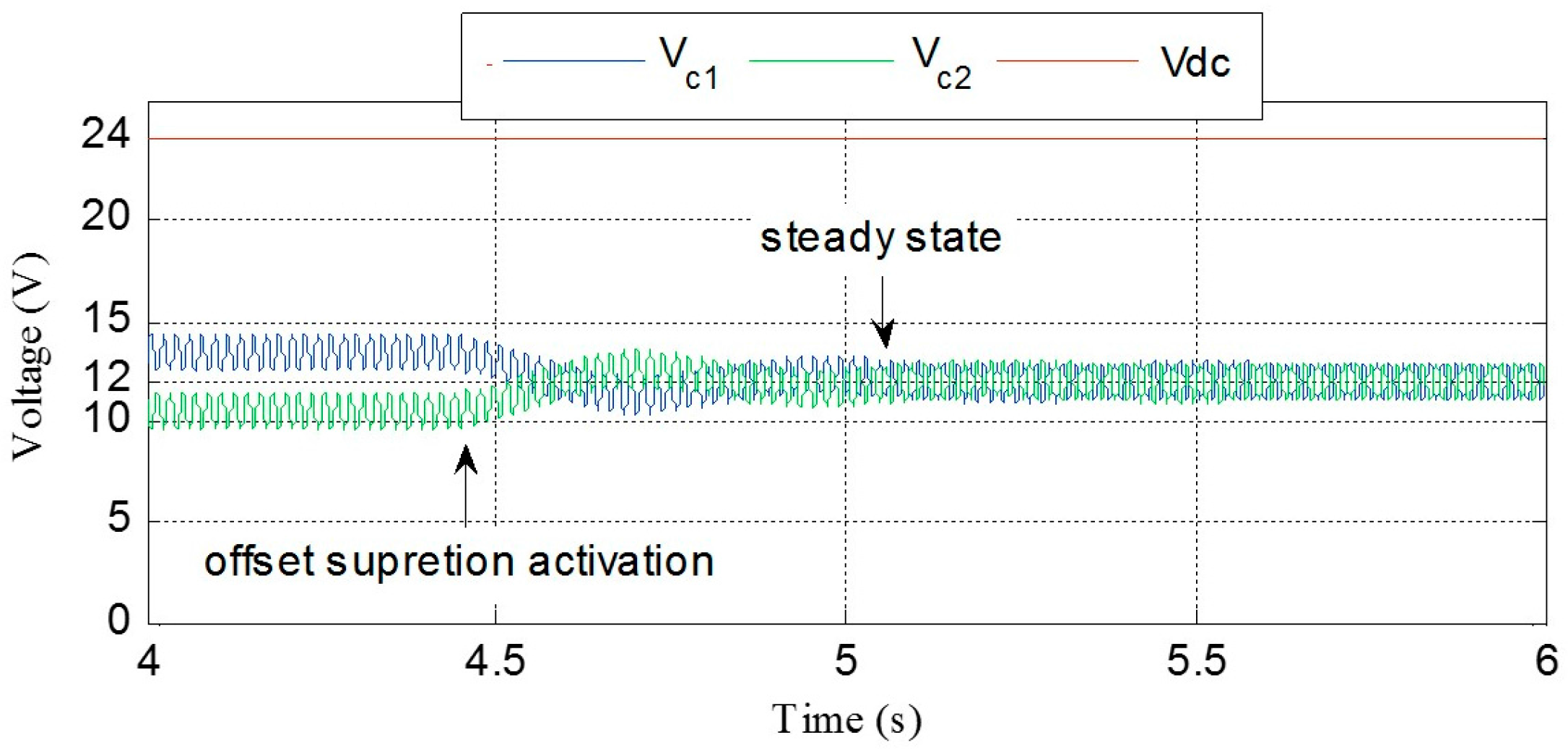
4.1. Simulation Studies

The proposed control scheme has two important roles: the first is to control and balance the generated two-phase voltage, and the second is to eliminate the DC-link capacitors’ offset voltage caused by PI controllers which add DC to the produced voltage low. To evaluate and to choose the PI voltage controllers’ gains, a simulation test was done at the speed of 200 rpm using kp = 2.2 and kI = 600 obtained from many simulation testes. Figure 5 shows the phase voltage and current trajectories in the α-β reference frame at 200 rpm operation. It shows that the delivered voltage as well as the obtained current are perfectly balanced, which is achieved by the 4S3P inverter output voltage control.
The output of the PI voltage controllers is a combination of a sinusoidal term used to ensure reference voltage tracing, and a direct component which comes from the voltage sensors’ offset, from the unbalance of the DC-link capacitor voltage and from PI controllers that usually control direct quantities. The dc PI output component leads to a disturbance in the DC-link voltage by adding an offset voltage. This phenomenon can lead to the system breaking down if one of the capacitors reaches a low voltage value. In the proposed voltage control scheme, a low pass filter is added in order to extract the direct component, additionally, this component is subtracted from the reference voltage. This voltage offset suppression strategy is confirmed by simulation when the PMSM is under a load at the speed of 800 rpm. The results are shown in Figure 6. The voltage offset had been obvious before applying the suppression method. After the voltage offset suppression algorithm is triggered at t = 4.45 s, the two-capacitor voltages converge to 12 V at t = 5 s, flowing through a transient state.
Conclusively, it can be confirmed by simulation that the proposed scheme ensures a balanced inverter output voltage and current as well as dc link voltage offset suppression.

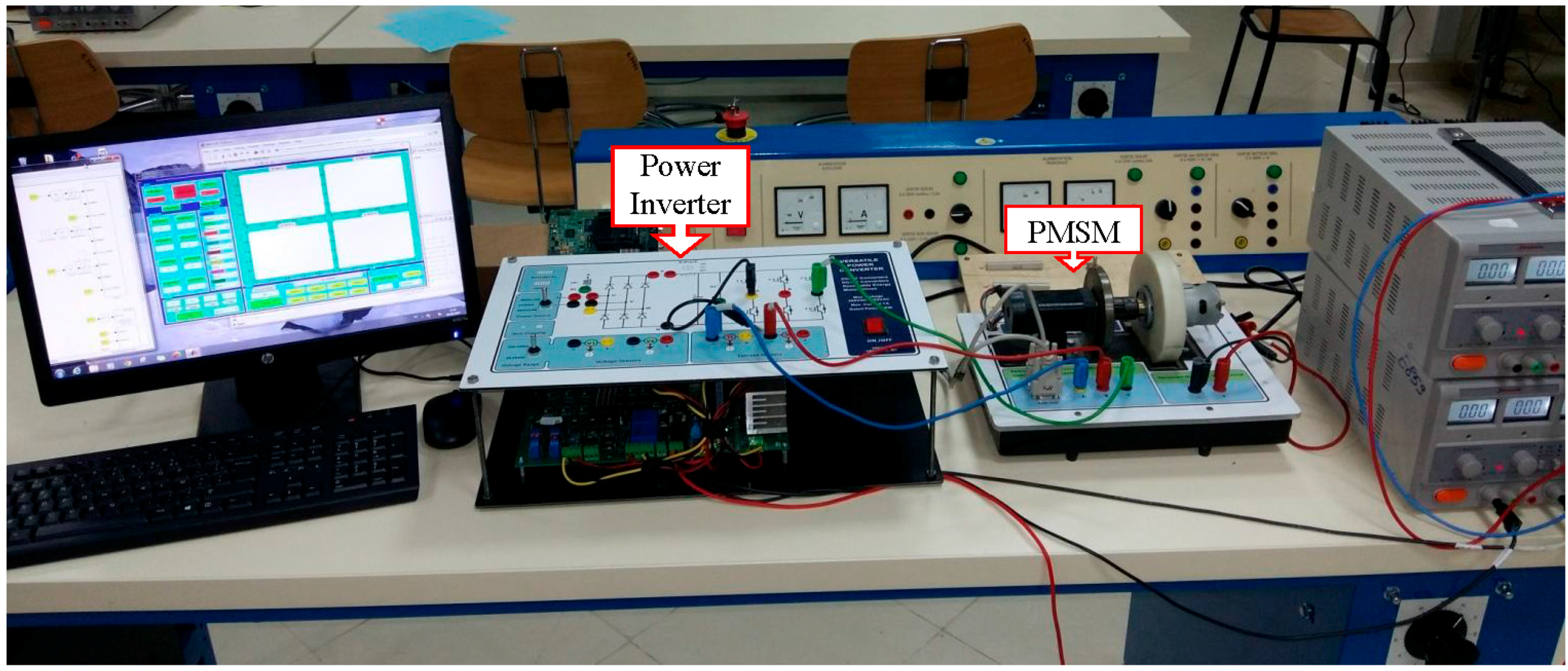
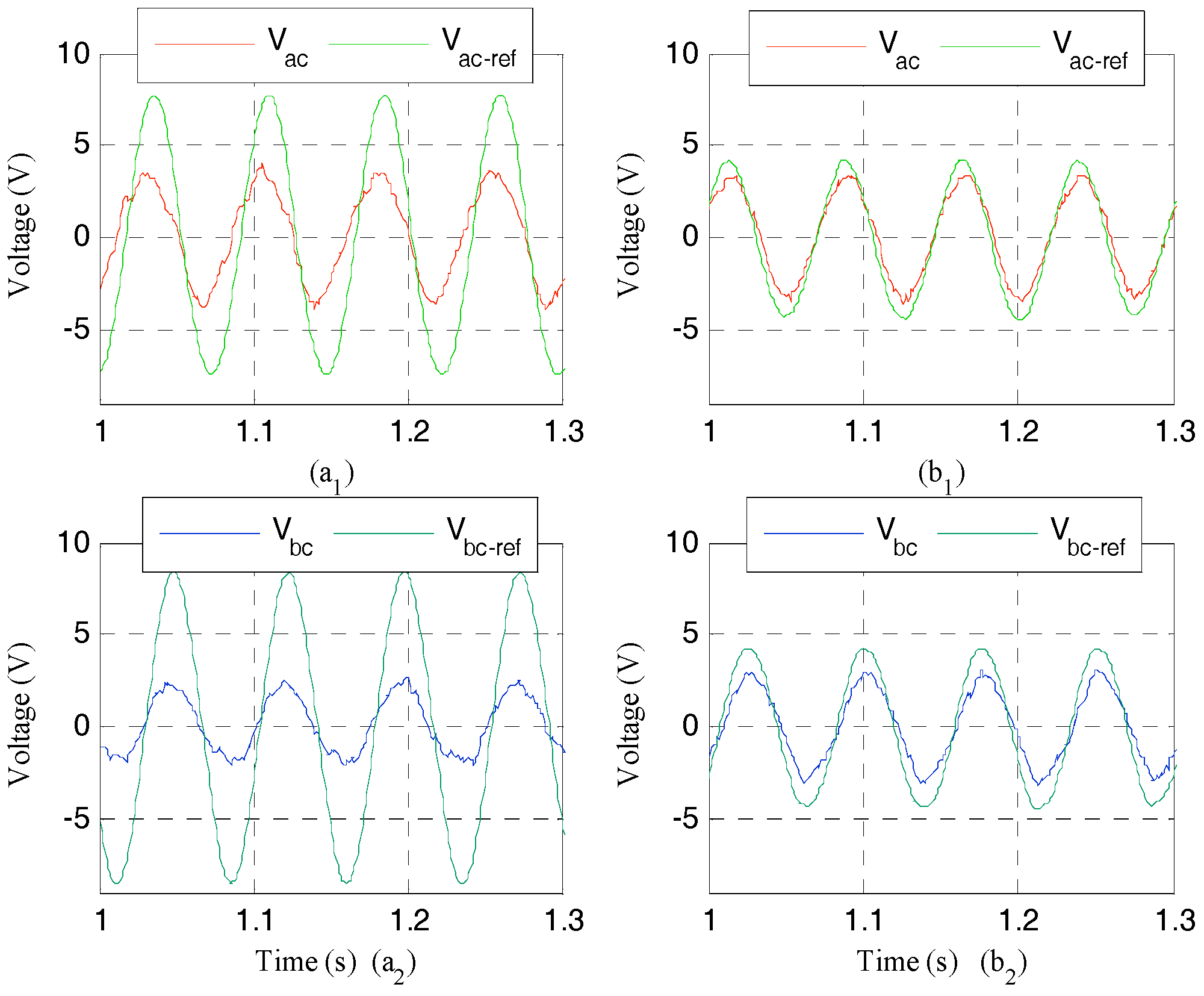
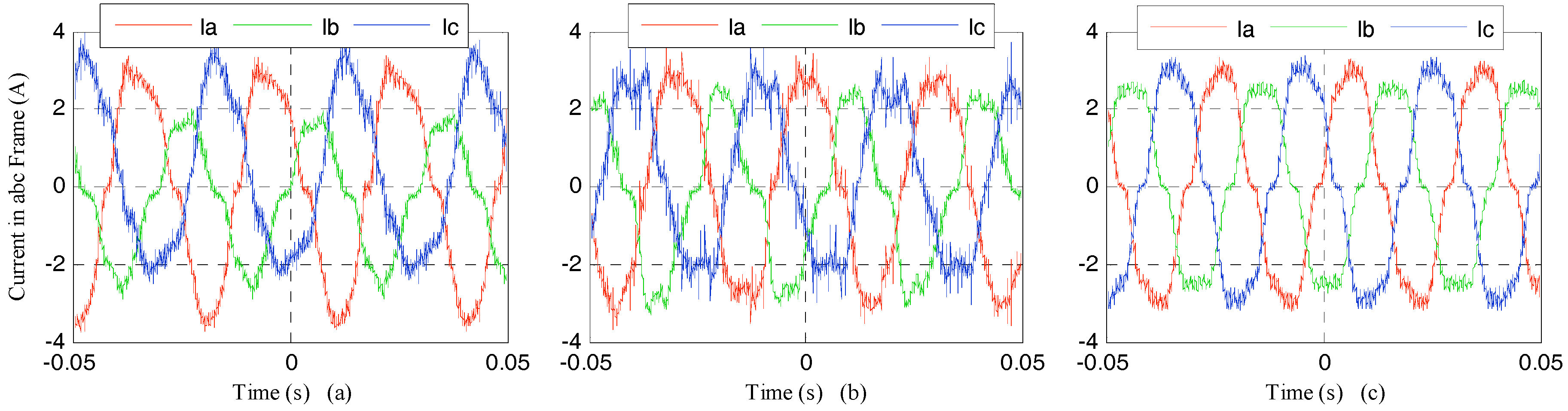
4.2. Experimental Evaluation

After simulation of the proposed DC-link capacitor voltage offset suppression and the 4S3P inverter output voltage control scheme algorithms, the experimental evaluations have been carried out in the experimental setup presented previously on an 80 W industrial PMSM. During experimental tests, we started by adjusting PI controllers gains for loaded PMSM at 200 rpm. The simulated PI controller gains have been taken as a first trial value; those gains are experimentally adjusted using trial and error until discovering the best performance. The PI controllers’ performance is showed in Figure 7. It is obvious, from Figure 7(a1,a2), that when the standard control algorithm of the 4S3P inverter topology is used, the output voltages’ waveforms are non-ideal since the generated voltages are not following the reference voltages; as a result, it can lead to the over modulation at low speed. However, once PI controllers are triggered, the 4S3P output voltages are monitored to follow the references’ voltages as is depicted in Figure 7(b1,b2). The three-phase current form, at 500 rpm and when the PMSM is under a load, with and without the proposed control method and with a standard 6S3P inverter, is shown in Figure 8. It can be noticed from Figure 8a that the current is unbalanced when a 4S3P inverter is used; it is caused by the DC-link capacitor voltage fluctuation, and one can note that ib is significantly smaller than the others, and there is almost no phase difference between ia and ic. Therefore, the torque pulsation is very significant at the normal operation. Conversely, that torque is smooth with the compensation method in Figure 8b, as well as when a traditional 6S inverter is utilized Figure 8c.
Figure 9 shows the experimental results of the torque at 200 rpm when the machine is under load. The top row figures show the results of the torque behaviours in three condition; in the first, the PMSM is supplied by a 4S3P inverter controlled by an ordinary control algorithm Figure 9a; in the second, Figure 9b, the torque shown is generated using the proposed control scheme; and in the last one, Figure 9c presents the generated torque when the PMSM is fed by the 6S3P inverter. However, to quantify the distortion of the generated torque at 200 rpm, a FFT analysis using the Simulink tool with the fundamental harmonic of 13.33 Hz is done, and the results are shown in the bottom row figures. One can observe from those results that a second harmonic with 26.66 Hz is added to the produced torque with total harmonic distortion (THD) equals 36.8%. Nevertheless, when the proposed algorithm is applied, torque ripples are reduced to THD = 8.5%.
Figure 10 shows that a half-voltage variation is about 12 V. Also, note that vc1 and vc1 fluctuate in opposite directions since their sum (DC-link voltage) is kept constant Vdc = 24 V and opposite currents are flowed through capacitors.
With the proposed control scheme, the DC-link fluctuation is neither eliminated nor attenuated, but the fluctuations are kept at around half of the supply voltage which is the purpose of much research [20,21].
Figure 11 presents the speed tracking capability and reliability of the proposed algorithm. Indeed, starting from a steady state at 200 rpm, 1000 rpm acceleration and deceleration profiles were applied respectively at t = 2 s and t = 8 s. The results show that the proposed controllers guarantee efficient speed profile tracking and current harmonic elimination through the range speed, Figure 11c. In contrast, the current performance of the conventional scheme without compensation deteriorates significantly at low speed, due to the fixed PI gains and large sampling time compared to the voltage loop response time.

5. Conclusions

The important features required in an industrial inverter are low cost and high efficiency. In the 4S3P inverter, the cost-effectiveness has been ensured by using two split capacitors, since the middle point is reachable. However, this power converter topology suffers from a number of limitations such as a fluctuating capacitor centre tap voltage, which destroys the current balance particularly. In this work, PI controller based schemes were designed and utilized to ensure the output voltage balance. Moreover, low pass filters were used to eliminate the DC-link capacitors’ voltage offset. The effectiveness of the proposed algorithm is validated through a series of simulation and experimental tests. The results demonstrate that the generated voltages are balanced without disturbing either the normal operation or the DC-link voltage balance in the entire speed range. Furthermore, the direct and quadratic currents as well as the torque, are enhanced in terms of ripple and the second harmonic is highly mitigated.

Author Contributions

Fadil Hicham initiated the idea of the work. Ait Driss Youness conducted the literature review. Driss Yousfi prepared the experimental test bench. Mohamed Larbi Elhafyani supervised the work. All authors have read and approved the final manuscript.

Conflicts of Interest

The authors declare no conflict of interest.

References

  1. Van der Broeck, H.W.; Van Wyk, J.D. A Comparative Investigation of a Three-Phase Induction Machine Drive with a Component Minimized Voltage-Fed Inverter under Different Control Options. IEEE Trans. Ind. Appl. 1984, 20, 309–320. [Google Scholar] [CrossRef]
  2. Lee, D.-M.; Park, J.-B.; Toliyat, H.A. A Simple Current Ripple Reduction Method for B4 Inverters. J. Electr. Eng. Technol. 2013, 8, 1062–1069. [Google Scholar] [CrossRef]
  3. Pan, L.; Wang, B.; Su, G.; Cheng, B.; Peng, G. A Novel Space Vector modulation Scheme and Direct Torque Control for Four-switch BLDCM Using Flux Observer. J. Electr. Eng. Technol. 2015, 10, 251–260. [Google Scholar] [CrossRef]
  4. Lin, C.-T.; Hung, C.-W.; Liu, C.-W. Position sensorless control for four-switch three-phase brushless DC motor drives. IEEE Trans. Power Electron. 2008, 23, 438–444. [Google Scholar] [CrossRef]
  5. Trinh, Q.-N.; Lee, H.-H. Low Cost and High Performance UPQC with Four-Switch Three-Phase Inverters. J. Electr. Eng. Technol. 2015, 10, 1015–1024. [Google Scholar] [CrossRef]
  6. Welchko, B.A.; Lipo, T.A.; Jahns, T.M.; Schulz, S.E. Fault tolerant three-phase AC motor drive topologies: A comparison of features, cost, and limitations. IEEE Trans. Power Electron. 2004, 19, 1108–1116. [Google Scholar] [CrossRef]
  7. Errabelli, R.R.; Mutschler, P. Fault-Tolerant Voltage Source Inverter for Permanent Magnet Drives. IEEE Trans. Power Electron. 2012, 27, 500–508. [Google Scholar] [CrossRef]
  8. Freire, N.M.A.; Marques Cardoso, A.J. A Fault-Tolerant Direct Controlled PMSG Drive for Wind Energy Conversion Systems. IEEE Trans. Power Electron. 2014, 61, 821–834. [Google Scholar] [CrossRef]
  9. Lin, C.K.; Yu, J.T.; Lai, Y.S.; Yu, H.C.; Peng, C.I. Two-vector-based modeless predictive current control for four-switch inverter-fed synchronous reluctance motors emulating the six-switch inverter operation. Electron. Lett. 2016, 52, 1244–1246. [Google Scholar] [CrossRef]
  10. Nguyen, T.D.; Lee, H.-H.; Nguyen, H.M. Adaptive Carrier-based PWM for a Four-Switch Three-Phase Inverter under DC-link Voltage Ripple Conditions. J. Electr. Eng. Technol. 2010, 5, 290–298. [Google Scholar] [CrossRef]
  11. Kim, J.; Hong, J.; Nam, K. A Current Distortion Compensation Scheme for Four-Switch Inverters. IEEE Trans. Power Electron. 2009, 24, 1032–1040. [Google Scholar]
  12. Blaabjerg, F.; Neacsu, D.O.; Pedersen, J.K. Adaptive SVM to compensate DC-Link voltage ripple for four-switch three-phase voltage-source inverters. IEEE Trans. Power Electron. 1999, 14, 743–752. [Google Scholar] [CrossRef]
  13. Fadil, H.; Driss, Y.; Aite Driss, Y.; Elafyani, M.L.; Abd Rahim, N. Sliding-Mode Speed Control of PMSM with Fuzzy-Logic Chattering Minimization—Design and Implementation. Information 2015, 6, 432–442. [Google Scholar]
  14. Fadil, H.; Yousfi, D.; Driss, Y.A.; Nasrudin, A.R. Synchronization Techniques benchmarking of grid fault modes in single-phase Systems. In Proceedings of the Renewable and Sustainable Energy Conference, Ouarzazat, Morocco, 17–19 October 2014.
  15. Pillay, P.; Krishnan, R. Modeling of Permanent Magnet Motor Drives. IEEE Trans. Ind. Electron. 1988, 35, 537–541. [Google Scholar] [CrossRef]
  16. Dasgupta, S.; Mohan, S.N.; Sahoo, S.K.; Panda, S.K. Application of four-switch-based three-phase grid-connected inverter to connect renewable energy source to a generalized unbalanced microgrid system. IEEE Trans. Ind. Electron. 2013, 60, 1204–1215. [Google Scholar] [CrossRef]
  17. Zeng, Z.; Zheng, W.; Zhao, R. Performance Analysis of the Zero-Voltage Vector Distribution in Three-Phase Four-Switch Converter Using a Space Vector Approach. IEEE Trans. Power Electron. 2017, 9, 1732–1740. [Google Scholar] [CrossRef]
  18. Hu, Y.; Gan, C.; Cao, W.; Li, W. Central-Tapped Node Linked Modular Fault Tolerance Topology for SRM Based EV/HEV Applications. IEEE Trans. Power Electron. 2016, 31, 1541–1554. [Google Scholar] [CrossRef]
  19. Zeng, Z.Y.; Zheng, W.Y.; Zhao, R.X.; Zhu, C.; Yuan, Q.W. Modelling modulation and control of the three-phase four-switch PWM rectifier under balanced voltage. IEEE Trans. Power Electron. 2016, 31, 4892–4905. [Google Scholar]
  20. Wang, W.; Luo, A.; Xu, X.Y.; Fang, L.; Thuyen, C.M.; Li, Z. Space vector pulse-width modulation algorithm and DC-side voltage control strategy of three-phase four-switch active power filters. IET Power Electron. 2013, 6, 125–135. [Google Scholar] [CrossRef]
  21. Wang, R.; Zhao, J.; Liu, Y. A comprehensive investigation of four-switch three-phase voltage source inverter based on double Fourier integral analysis. IEEE Trans. Power Electron. 2011, 26, 2774–2787. [Google Scholar] [CrossRef]
Figure 1. Power circuit of the four-switch three-phase inverter.
Information 08 00011 g001
Figure 2. Vector diagrams.
Information 08 00011 g002
Figure 3. Vector diagrams.
Information 08 00011 g003
Figure 4. Experimental setup including 80 W PMSM and a power inverter.
Information 08 00011 g004
Figure 5. Simulation of voltage and current trajectories in the α-β reference frame at 200 rpm; (a,b) are the voltage and current wave form without voltage regulation; (c,d) are the voltage and current wave form with the proposed voltage control scheme.
Information 08 00011 g005
Figure 6. Simulation result of the capacitors’ voltage Vc1, Vc1 and Vdc behaviors at the activation of the voltage offset suppression, at 800 rpm.
Information 08 00011 g006
Figure 7. Experimental results at 200 rpm of controlled 4S3P output voltages compared to their references: (a1,a2) are without compensation; (b1,b2) are with the proposed scheme.
Information 08 00011 g007
Figure 8. Experimental waveforms of the three-phase motor current Ia, Ib and Ic, when the load is applied at 500 rpm. (a) Motor phase current with the standard control scheme; (b) Motor phase current with the proposed control scheme; (c) Motor phase current when the six-switch three-phase inverter is used.
Information 08 00011 g008
Figure 9. Experimental waveforms of the motor torque and their frequency analyses under a load at 200 rpm. (a) With the standard control scheme; (b) With the proposed control scheme; (c) When the six-switch three-phase inverter is used.
Information 08 00011 g009
Figure 10. Capacitor voltages’ fluctuation at 200 rpm when the proposed control scheme is applied.
Information 08 00011 g010
Figure 11. Experimental result of speed profile following. (a) Reference and measured speed; (b) motor currents in the d-q frame without compensation scheme; (c) motor currents in the d-q frame with the proposed scheme.
Information 08 00011 g011
Table 1. Inverter and controller parameters.
ComponentsValuesComponentsValues
DC-voltage24 VDC-link upper capacitor C14400 µF
PWM frequencyFPWM = 12 kHzDC-link lower capacitor C24400 µF
SamplingFs = 10 kHzInverter rated power1 kW
Table 2. PMSM parameters.
ComponentsValuesComponentsValues
Rated powerp = 80 WPole pairs4
Rated speed4000 rpmViscous frictionfr = 0.04·10−3 Kg·m2
Resistance and inductanceR = 0.43 Ω, L = 1.35 mHRotation inertiaJ = 0.5·10−3 Nm/rad

