1. Introduction
Using FPGA-based development platforms proved to be a wise choice for practice sessions in subjects that are typically included in a standard academic digital design curriculum, covering basic to advanced levels [
1,
2,
3,
4]. These platforms facilitate coordination between subjects and allow the implementation of projects that share common backgrounds, but are described and/or specified at varying levels of abstraction and complexity [
5].
In recent years, the teaching of electronics has seen a significant increase in the availability and variety of remote laboratories [
6,
7,
8]. The need for these resources is evident in off-campus learning [
9,
10,
11], while in on-campus teaching, they become a viable option to meet the growing demand for laboratory resources beyond regular class hours, which are often very limited. A great variety of remote laboratories were proposed [
12,
13,
14,
15,
16,
17,
18,
19,
20,
21]. In this context, the authors developed their own remote laboratory (RLAB). Its main feature is that it does not need a webcam for its operation. This allows the users to verify their designs remotely on the real hardware, even if they do not have a broadband connection capable of supporting real-time video transmission. The initial version, based on Arduino, was introduced in [
22], and subsequent improvements were made since then, including a migration to a system based on a Raspberry Pi 4. This web-based application enables users to remotely configure an FPGA-based development platform that has a wide range of peripherals, and allows interaction with these components in order to facilitate design debugging and testing, mirroring the experience of working directly on campus.
The RLAB was used for the last three academic years in two different courses (Digital Electronics and Electronic Systems), as part of the Robotic and Mechatronic Electronics Degree (GIERM) at the University of Málaga, to complement (rather than replace) on-campus teaching, in response to the growing need for access to laboratory resources beyond regular teaching sessions. An initial version of the RLAB tool was offered to students in 2020/21, showcasing its usefulness in both courses. The usefulness of the tool became especially apparent in the hybrid teaching situation imposed by restrictions during the pandemic. Students experienced an improved version of the tool in 2021/22 and 2022/23. Each academic year saw the list of projects increase with new design proposals or improved versions of the initial projects.
In this paper, we share our first-hand experience in the Digital Electronics course. Historically, practical sessions in this course involved using the Digilent Nexys3 platform [
23].
Practical work in this subject primarily revolves around projects focused on basic logic design primitives and functional blocks (both combinational and sequential), as commonly taught in introductory Digital Electronics courses. Designs are mainly described at a schematic level, and are simulated and verified using the Xilinx ISE Design Suite environment. The design is verified on the platform once the FPGA configuration file is generated and uploaded. Typically, the platform’s switches, buttons, and expansion ports for peripherals (such as PmodTM modules including a hexadecimal keyboard, encoder, etc.) serve as the input interface. The output interface consists of display elements such as LEDs and seven-segment displays. It should be noted that this verification step can also be carried out using the remote laboratory tool.
Firstly, this article provides a brief overview of the RLAB tool and introduces the strategy used to incorporate it in projects for the Nexys3 platform. Secondly, it outlines specific proposals for practice sessions that align with the program’s level of complexity and timeline, and with the philosophy of the Electronics Design course. Finally, the article discusses the impact, reception, and evaluation of the remote laboratory tool, including information taken from a satisfaction survey presented to students at the end of the semester. Suggestions for improvement based on the survey findings are also presented.
2. Using a Remote Lab: Strategy for the Implementation of Design Projects
As mentioned before, our remote lab for FPGA aims to optimize bandwidth requirements by eliminating the need for webcams to verify system behavior. This is achieved by having the system use a set of modules that allow the development board peripherals to be excited and monitored from a Raspberry Pi 4, which also functions as an application server in the current version. These modules are carefully designed for seamless integration in the development environment, providing students with a smooth, uninterrupted experience.
The Nexys3 development board’s basic input/output peripherals are accessed through the server by efficiently reading and writing status registers, ensuring effective communication between server and client. Additionally, the Raspberry Pi 4 can simulate the behavior of several external peripherals through its digital input/output pins connected to the expansion ports of the Nexys3 board. This is a significant advantage of this remote laboratory as it saves costs on hardware modules.
Users access the remote laboratory via a web-based application that manages access control and allocates usage time. The FPGA configuration file is transferred to the system when logging in, allowing verification of the digital design. To facilitate the design verification process, graphical components, such as virtual switches, push buttons, LEDs, and seven-segment displays, serve as virtual input and output peripherals.
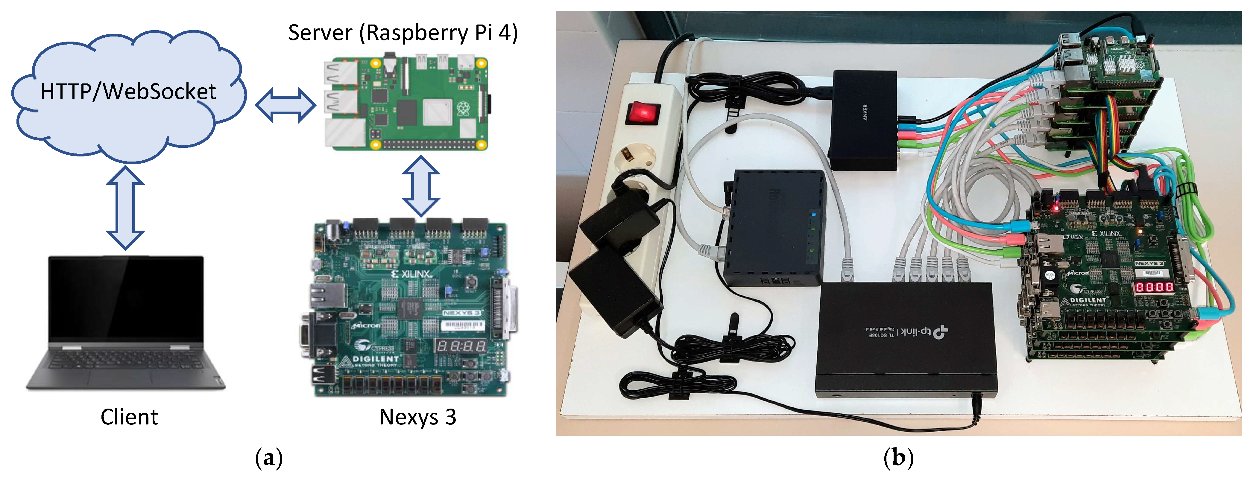
Figure 1 provides an overview of the architecture of the remote laboratory and shows an image of the system. The server consists of a cluster of Raspberry Pi 4s connected to Nexys3 boards, which can be easily scaled if necessary.
This is the setup that the user physically interacts with when accessing the web portal.
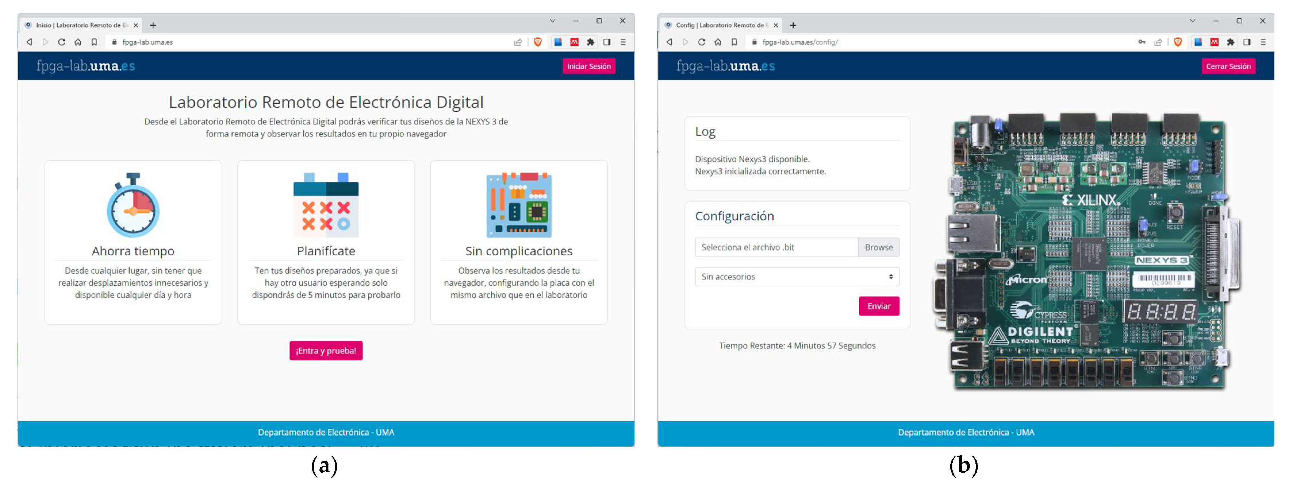
Figure 2 shows two screens of the web-based application and its interface.
Carrying out practice projects using the Nexys3 platform in the remote laboratory requires a functional block, known as “Remote_Lab”. This module, developed in VHDL, allows serial communication between the application server implemented on the Raspberry Pi4 and the Nexys3 board itself. On the one hand, it receives the status of the input peripherals that the user establishes from the web application (switches, push buttons, etc.). On the other hand, it analyzes the signals that stimulate the output peripherals, informing the server when a change occurs so that it can be updated on the user’s screen.
Using a pre-existing project template called RLAB_Plant is recommended when carrying out the practice projects in order to simplify the task for students. This template consists of the Remote_Lab module, which is connected to another module called MyDesign.
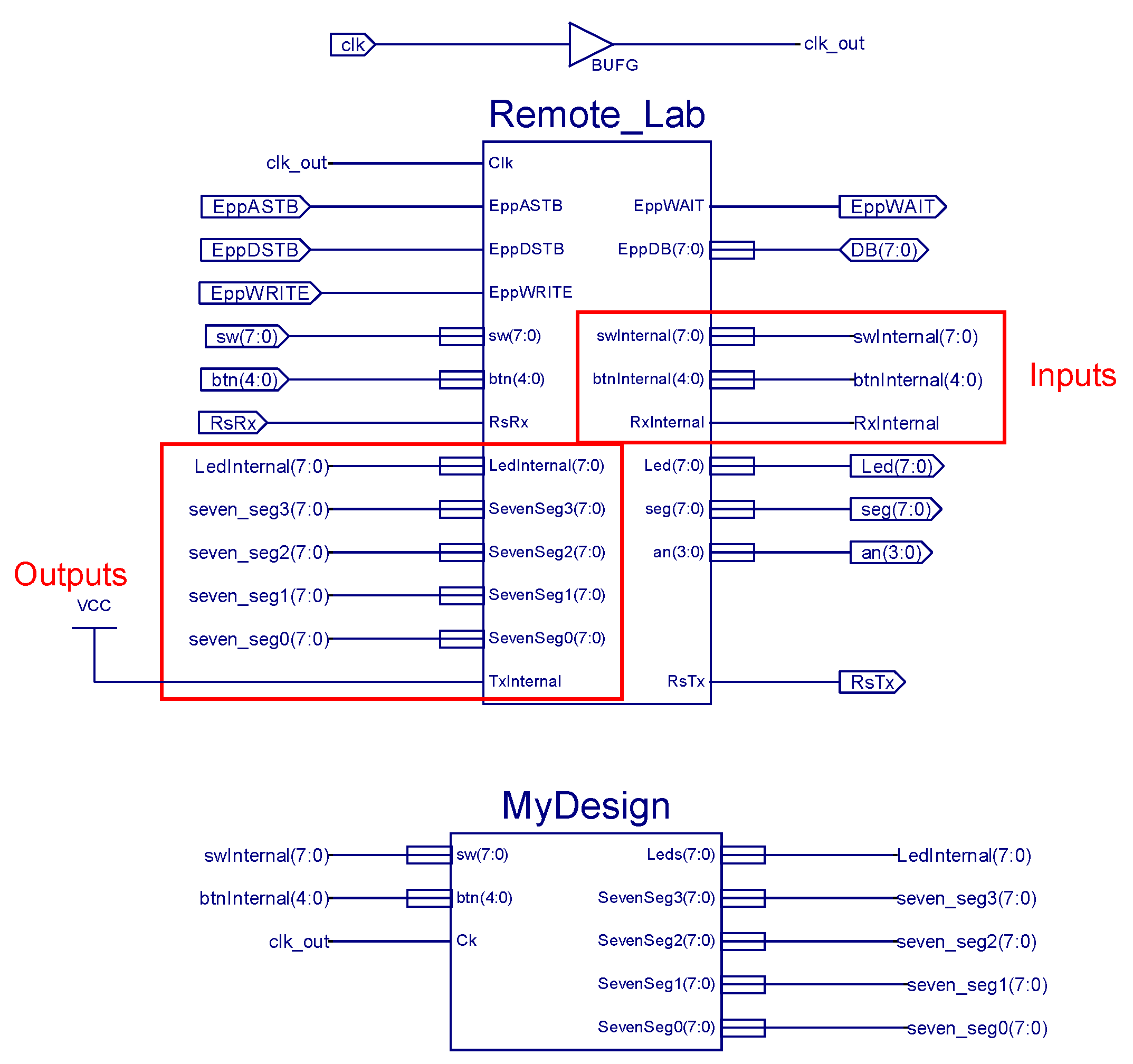
Figure 3 shows the highest-level schematic of this project (top.sch), which does not require any modifications. The design of each practice project should be integrated into the MyDesign module.
Figure 3 also shows the Remote_Lab module’s input/output interface. This module serves as a bridge, with inputs and outputs for communication between the web server and the external interface. It also establishes connections with the switches, buttons, seven-segment displays, and LEDs of the Nexys3 platform. By replicating the board’s connections, the Remote_Lab module allows interaction with the implemented design from both the physical platform and the remote laboratory environment. The MyDesign module is a blank design sheet with only the signal connector symbols representing the input/output ports. Note that the inputs and outputs marked in red in
Figure 3 are the inputs and outputs of the MyDesign module, respectively. Students can standardize their use of the remote laboratory by focusing on designing the proposed system and selecting the appropriate interface signals. This approach streamlines the process and facilitates a consistent workflow for students.
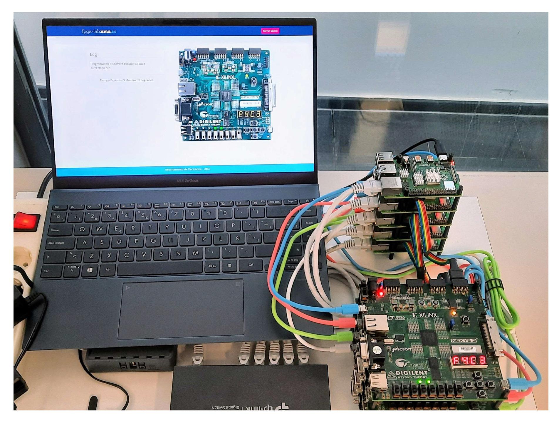
Figure 4 provides an example of how the Web Client Interface shows what is happening in the physical setup. Note that the state of LEDs and seven-segment displays are the same in the web application and the physical board, which happens in real time.
3. Practice Proposal
The Digital Electronics course, as part of the degree program, focuses on the fundamental principles of logic design, starting from logic gates and combinational functional blocks, and progressing to sequential design involving counters and register blocks and state machine analysis and synthesis. The practical training approach aims to promote the development of engaging designs that are of suitable complexity for students. The philosophy underlying the proposed projects is to provide a starting project design of medium complexity that encompasses modules for students to be designed and verified based on given specifications, ready to be incorporated in the full project. Once incorporated and implemented in the FPGA platform, students can verify the correct operation of the system by interacting with the peripherals and the platform’s inputs and outputs. This process of debugging and validating the design can be carried out in the on-campus laboratory or via the remote laboratory, before being presented to the instructor in a face-to-face session. These practical session tasks are intended to complement the theory-based and practical aspects covered in the course curriculum, providing a comprehensive learning experience.
The projects presented in this section include: (1) an electronic voting and tallying system; (2) a reconfigurable signaling beacon with four warning light signals, including a Morse code SOS signal represented by short and long flashes; (3) a system for controlling the automatic opening and closing of a door from on sensor status; and (4) an extension of the last project in which the opening and closing of the door are controlled by an access code validation assigned to users. The paragraphs below set out specific proposals to develop these projects in the practice sessions, and detail the design tasks entrusted to students, highlighting the option of using the remote laboratory for design debugging outside of regular class hours. Projects (1) and (3) were proposed as examples in Digital Electronics in the academic year 2020/21. Two new projects were added during academic years 2021/22 and 2022/23, one as a new project (2) and the other as an extension of the previous proposal (4). The projects, which were integrated into the laboratory sessions scheduled throughout the semester, consisted of a total of 12 sessions, with each session lasting 1.5 h. For each project, students are provided with a guide describing expected system behavior and specifications, design activities, and specific tasks they should perform during the practice sessions.
It is important to note that the first three laboratory sessions are devoted to working with a tutorial (practical session 0). This tutorial allows students to familiarize themselves with the fundamental principles and philosophy of the working environment, such as schematic capture, test vector generation, and simulation. Students also receive a Webpack license for the Xilinx tool, allowing them to work on these assignments from home. This includes the final phase of implementation on the Nexys3 platform, where the remote lab is a very useful resource (mainly for debugging and verification of system functionality), before presenting their work to the instructor for final review in the laboratory.
3.1. Project 1: Electronic Voting and Tallying System
The project, Vot_RL, focuses on implementing a voting system capable of logging votes from eight voters, tallying them using a qualified majority decision and presenting the results. In this project, eight switches from the Nexys3 board are assigned for voter selection, and two buttons (left and right buttons in Nexys3) are designated for casting votes (for or against). The results are displayed using the seven-segment displays and LEDs in Nexys3. Another button (middle button in Nexys3) is used as the main system on–off (reset).
As an example,
Figure 5 shows two images of the voting process conducted in the remote laboratory.
Figure 5a shows the system when voter 4 is selected by turning on switch 4 in Nexys3, waiting for the vote to be cast by pressing one of the two buttons: for (left) or against (right). The selected voter is indicated by the active switch’s LED, which goes off once the vote is counted.
Figure 5b shows the conclusion of the voting process when all votes are cast. In this specific case, a ‘for’ result is indicated by the three leftmost LEDs lighting up, showing the results (seven votes for, one against). The system also ensures that only one voter can be selected at a time, and prevents a voter who already voted from voting again.
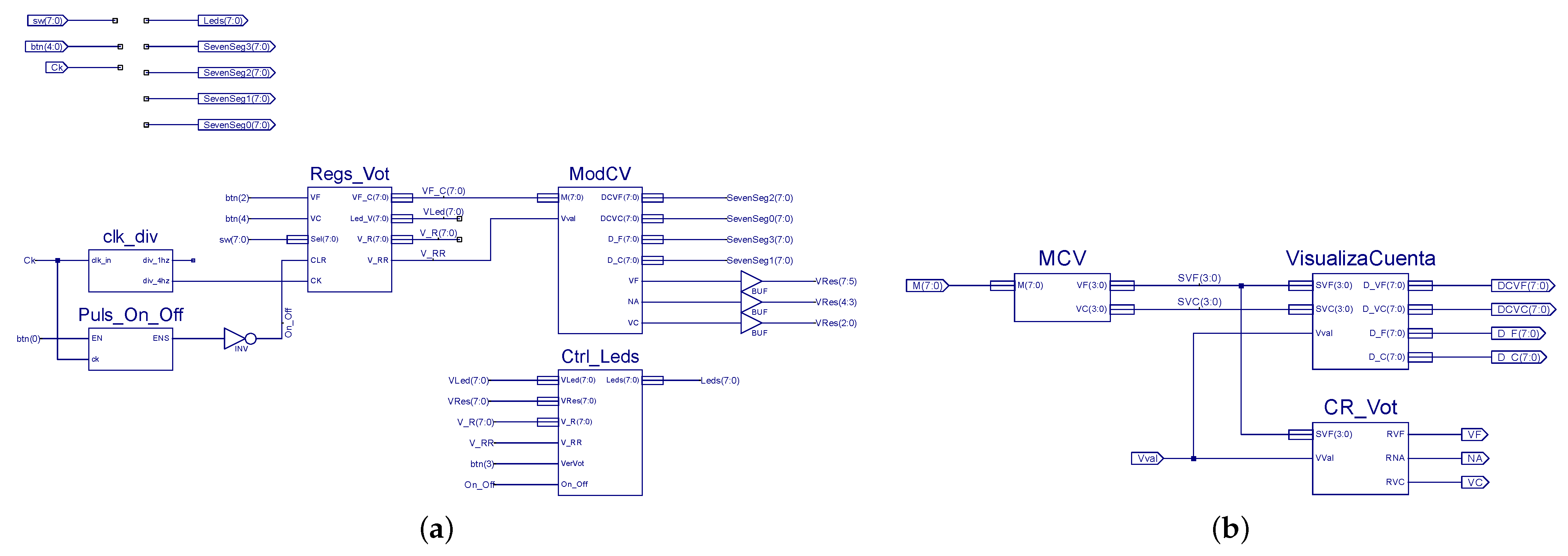
Figure 6a shows the block diagram schematic for the MyDesign module of the Vot_RL project provided to students. This design serves as the starting point for students’ work. The Clk_div block is in charge of generating an appropriate 1 Hz clock for the sequential blocks. Meanwhile, Puls_On_Off is used to synchronize the on/off button of the system. Ctrl_Leds is a combinational block that visualizes the appropriate status information in the Nexys3 LEDs. The key module within this design is the ModCV. It is intended to be designed by students as a combinational module responsible for tallying the votes and displaying the results. Meanwhile, Regs_Vot is a sequential module that controls the voting sequence and stores the voting information for each vote cast. Since the overall design includes both combinational and sequential modules, and given that analyzing and designing sequential blocks is still yet to be introduced when this project is presented to students, the design tasks are distributed in two phases: an initial phase addressing the design of the ModCV module as a fully combinational block, and a second phase addressing the complete project, carried out after the sequential systems are introduced.
Some support is provided in order to design the ModCV module. Students are advised to follow the block diagram provided in
Figure 6b. This approach involves dividing the module into three simpler combinational blocks, each implementing a specific function. MVC evaluates the number of votes cast (for/against), CR_Vot provides the final vote, and VisualizaCuenta generates the signals to visualize the voting results in the seven-segment displays. This design phase also includes validating the complete ModCV module by generating test vectors and simulating in the ISE Design Suite environment and in Nexys3.
The tasks proposed for the second phase are:
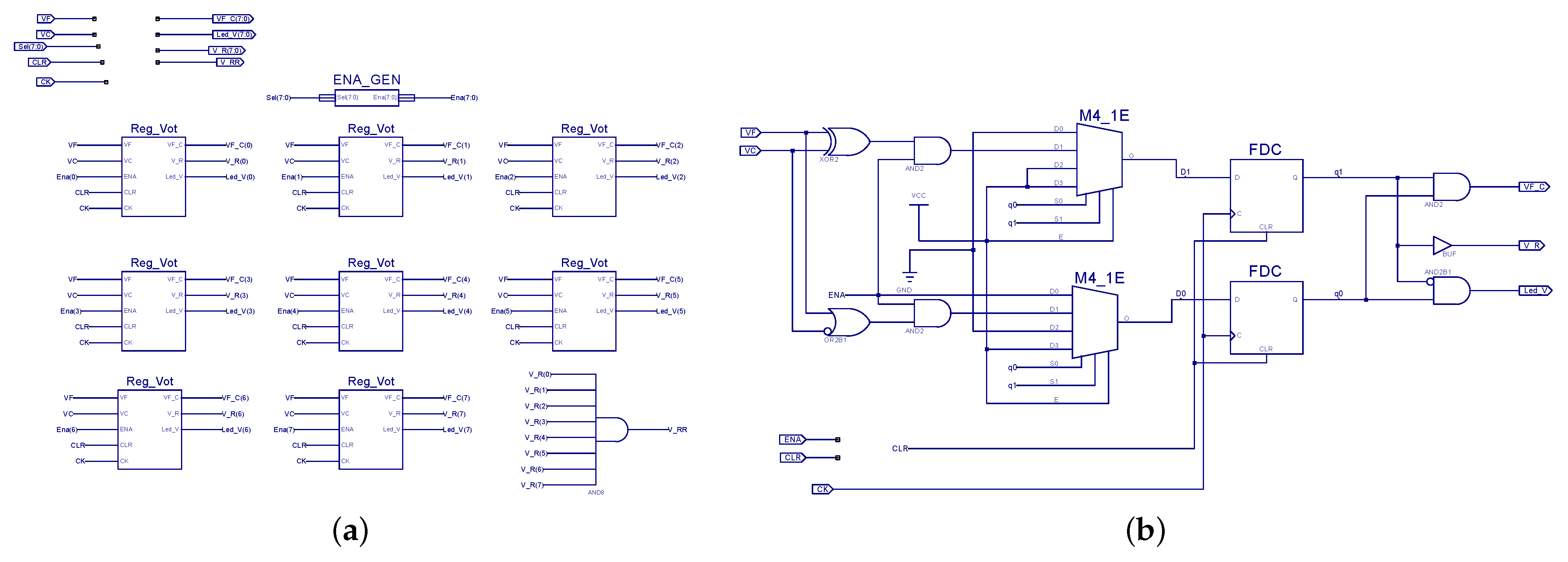
As an additional task, students are required to analyze the main sub-module in Regs_Vot, named Reg_Vot in
Figure 7a. The schematic diagram for this module is shown in
Figure 7b. This design is based on Xilinx library building blocks, such as logic gates, multiplexer (M4_1E: 4x1 Mux with enable input), and D flip-flops (FDC). This module acts as the state machine that controls the voting sequence and its registration process. For the Reg_Vot module, students should analyze the circuit in
Figure 7b and obtain its state transition diagram. This analysis will provide information on how the state machine operates and how it manages the voting process.
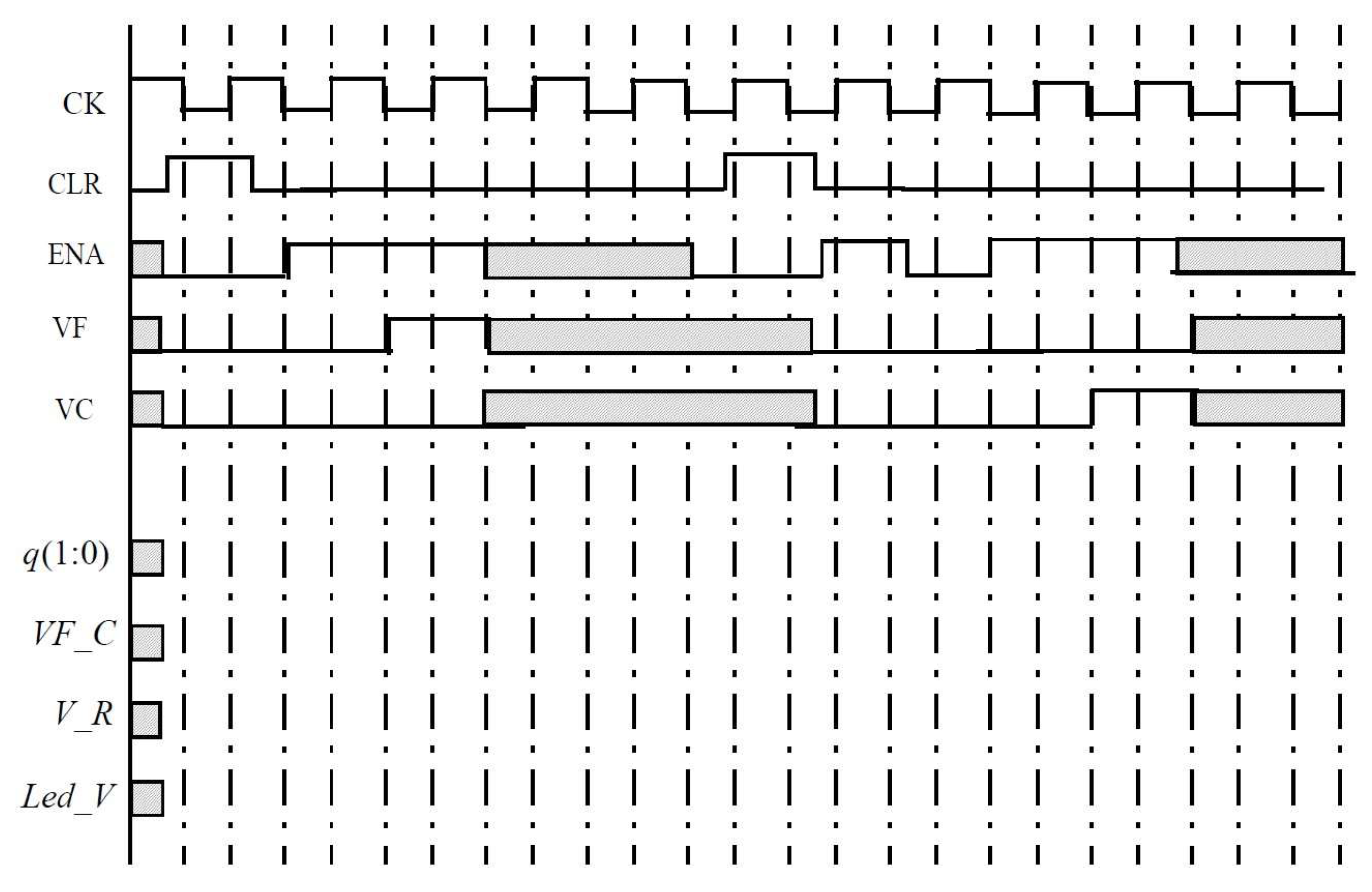
They also should simulate the Reg_Vot module and show its behavior using a timing diagram for a given input sequence. An example of a chronogram with a test sequence is provided to help students write an appropriate test vector file to simulate the behavior of the block (
Figure 8). In this figure, CLR is the clear input signal of the system, ENA is the enabling/selection input of the Reg_Vot module, and VF and VC are the inputs that indicate the vote (for or against), respectively. The output signals q(1:0) are a bus that represents the current state of the state machine, VF_C is the output that records the vote (VF_C = 0 against, 1 for), V_R is the signal that indicates whether the vote was finally taken or not, while Led_V is a signal that visualizes the voting process, as indicated above. After carrying out a previous analysis, the student must complete the chronogram in
Figure 8 and verify that the chronogram resulting from the simulation coincides with the expected one.
At the end of these practice sessions, students should have a comprehensive understanding of electronic voting systems as a whole and the role assigned to the different functional blocks that make up the overall design, both combinational and sequential. They should have also acquired experience in designing combinational blocks (including ModC, Ctrl_Leds) and in analyzing state machines (Reg_Vot) and verifying their functionality through simulation, as a practical example of the traditional problems proposed and solved in class sessions.
3.2. Project 2: Luminous Beacon with Four Selectable Warning Signals
The BCON_RL practice project focuses on implementing a luminous signaling beacon with four selectable warning signals.
Figure 9 shows the block forming the highest-level architecture in the MyDesign module of the proposal. Clk_div and Puls_On_Off are the same blocks in Project 1. VDisplays is a combinational block that shows the appropriate status information in the Nexys3 LEDs and seven-segment displays.
The student’s main task is to design the combinational modules in MSignal, which implements the different warning light signals.
Figure 10a shows the architecture proposed for the design of the MSignal module.
The main idea is to generate different sequences of output patterns from a five-bit binary counter output (cb5c block, five-bit counter, in the Ctrl module in
Figure 10b), which can be selected using a Nexys3 button. Different patterns can be considered, e.g., stand_by (ST_BY module), road_widening (Sh_OpenM), road_narrowing (Sh_CloseM), and SOS Morse code (SOS_MC). All these signals can be implemented by making the Nexys3 LEDs shift or blink in a periodic sequence following the selected pattern. Another two-bit counter (CB2CE, from the Xilinx digital library in the Ctrl module in
Figure 10b) is used to select one of four visualized signals. The last counter is controlled by a button in Nexys3 (Nivel_a_Pulso block in Ctrl module is in charge of synchronizing the button). The MSignal module also includes basic combinational blocks as a D2_4E decoder and M4_1E 4x1 multiplexer for eight-bit buses, both from the Xilinx digital library).
The full system works as follows: initially, the system is off, meaning the LEDs and seven-segment displays in the Nexys3 are turned off. The system is turned on by pressing the middle button. Then, the ST_BY signal is shown in the LEDs in Nexys3, and 0 is shown in the seven-segment displays to indicate the selected mode. Modes 1 to 3 can be selected by pressing the upper button in Nexys3.
As an example,
Figure 11 shows the result of a simulation where an SOS Morse sequence (dot, dot, dot, dash, dash, dash, dot, dot, dot) is generated by the SOS_MC block. For simplicity, one count of the counter signal cnt[4:0] is assigned to a dot and three counts to a dash. The period of the sequence is 32 clock cycles.
As in the previous project (1), since the overall design includes both combinational and sequential modules, and given again that analyzing and designing sequential blocks is yet to be introduced when this project is presented to students, the design tasks are distributed in two phases: an initial phase addressing the design of the MSignal module as a fully combinational block, and a second phase addressing the complete project, carried out after the sequential system is introduced.
The first design phase also includes validating the complete MSignal module by generating test vectors and simulating in the ISE Design Suite environment.
The tasks proposed for the second phase are:
Integrate the MSignal module with the other modules in the project.
Revisit the schematic diagrams of the other modules in order to understand their mission throughout the system.
Analyze and simulate the Nivel_a_Pulso sequential module, and understand its role as pushbutton synchronizer.
Implement and verify the design on the Nexys3 platform.
By the end of these sessions, students will have a comprehensive understanding of the project as a whole, including overall structure and subblocks partition. They should have also acquired experience in combinational design and in the analysis and use of sequential blocks as counters, or simple sequential design in button management, including the synchronization of external inputs (Puls_On_Off block in
Figure 9, and Nivel_a_Pulso in
Figure 10b). As the outputs in this project are light signals that evolve over time, it is difficult to show their operation in a static image.
Figure 12 shows a sequence pattern of one of the operation modes (Sh_OpenM).
3.3. Project 3: Automatic Door Opening/Closing Control System
The aim of the Door_RL practice project is to design a system that controls the automatic opening and closing of a door. The full system works as follows: the system has two operating modes (manual or automatic), selectable by means of an M selection input. The door is normally open in manual mode, and only remains closed while pushbutton P is pressed. The door is normally closed in automatic mode. It will open and remain open as long as presence is detected (PD signal is active); or, in the event of an inactive PD, if pushbutton P is pressed, which in this case is interpreted as a pulse. If the door is open and no presence is detected, it can be closed manually by pressing pushbutton P; failing this, it will close automatically when the opening time limit, as set in the timer, is reached. Note that in this case, the P signal acts as a pulse that commutates the status of the door (opening/closing and vice versa).
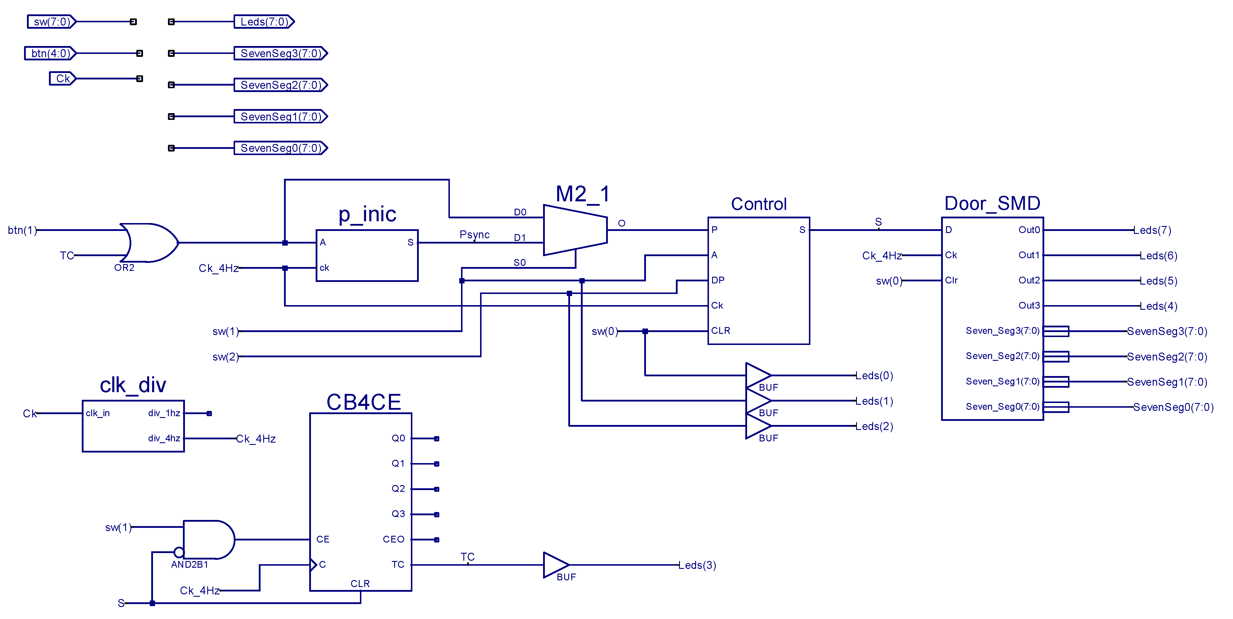
The schematic diagram for the MyDesign block for this project is shown in
Figure 13, indicating the elements that make up the control system. Students are provided with the design for all blocks except the control module, which they are responsible for designing and validating in this practical session.
As an example,
Figure 14 shows the result of a simulation of the Control module for a given sequence provided as in
Figure 8.
In
Figure 14, after CLR (active low pulse), the door is open (S, low), and after one clock cycle, automatic mode is activated (A, high) and remains high all the simulation time. Then, two P pulses arrive while DP is low, so the first P pulse closes the door (S goes high), and the second one opens it (S goes low again). When a new P pulse arrives, DP is also active (DP high), so the door remains open. The following P pulse closes the door because now DP is low again. Finally, a new activation of DP does nothing because the door is already open.
One of the components of the design (the Door_SMD module) emulates the opening and closing action of the door, with status visualized in the seven-segment displays and LEDs of the Nexys3 platform. The four leftmost LEDs in the Nexys3 are on when the door is closed and off when open. During the change from open to closed (or vice versa), the LEDs go off or go on sequentially, emulating the door’s movement.
Note also that signal P plays two roles, which are selected from the multiplexer M2_1 in
Figure 13. Signal P is directly a level pushbutton that signals when manual mode is selected, and a one-clock cycle synchronous pulse when automatic mode is selected. The P_inic module in
Figure 13 is responsible for generating this synchronous P pulse from the level pushbutton signal. Meanwhile, the CB4CE counter module in
Figure 13 is used as a timer to generate a P signal to close the door when an open time limit is reached.
The main tasks for students in this project (Door_LR) are to:
Design the Control module as a finite-state machine based on the specifications provided in the practical training guide.
Verify the correct operation of the control module by simulating several given input sequences. This involves running simulations to observe the expected behavior of the door control system.
Incorporate the designed control module into the Door_RL project and verify system operation. Implement the complete design on the Nexys3 platform, and ensure that the door opens and closes automatically as intended.
By completing these tasks, students will gain hands-on experience in designing finite-state machines, verifying their functionality through simulations, and implementing the control system on the Nexys3 platform to observe real-world operation.
3.4. Project 4: Access Control by User Code Validation
The aim of the AccCtrl_RL practice project is to implement a system that controls access to a venue, enabling the opening or closing of the entrance door once users entered their assigned access codes. An access code sequence was assigned to each user in an initial version of the project (as presented here). These sequences were hard-wired. In new versions, the access code assignment could be programmed by a user, i.e., entered by the user and stored in the system in system configuration mode.
The full system works as follows: for simplicity, only two users are contemplated, and so we have two sets of open/close access codes. Each user has two access codes, one to open the door and the other to close it. The buttons of the Nexys3 are used to enter the access code, and they should be pressed in an orderly sequence. The opening code is made up of a sequence of three buttons, while the closing code is made up of a sequence of two buttons. The door’s status is closed after the system is turned on. This is shown in the seven-segment displays and in the four leftmost LEDs of the Nexys3 (as in project 3). To open the door, a user must be selected by turning the corresponding switch on in Nexys3. A valid user open access code sequence must then be entered. The progress of a valid sequence is shown by the three rightmost LEDs of the Nexys3 coming on sequentially. After the three buttons are pressed in a valid sequence, the status of the door changes, the word “open” is shown in the seven-segment displays, and the four LEDs of the Nexys3 located furthest to the left go off. A valid user access code sequence must now be entered to close the door. For both sequences, these will be aborted and reset to initial status if any of the buttons pressed are not as expected in this sequence step.
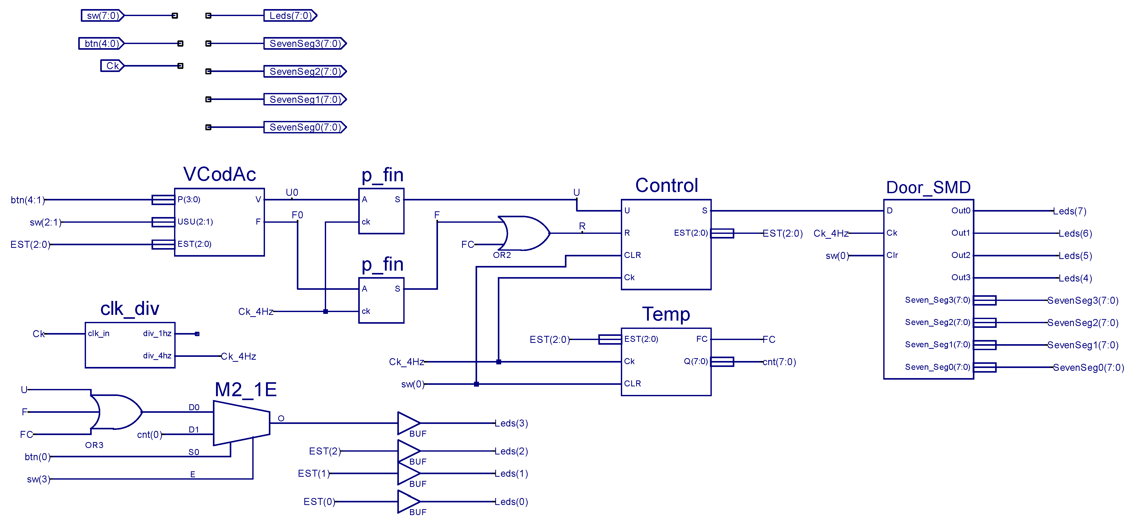
The schematic diagram for the MyDesign block for this project is shown in
Figure 15, indicating the elements that make up the control system. Students are provided with the design for all blocks except the Control module, which they are responsible for designing and validating in this practical session. Another main block in this schematic is VCodAc, a combinational module that checks whether the pressed button is as expected in each sequence step for each user.
Note that the Door_SMD module is also used in these projects to emulate the opening and closing action of the door, whose status is visualized in the seven-segment displays and LEDs of the Nexys3 platform. Note also that P_fin modules in
Figure 15 generate a one-clock cycle synchronous pulse from their own level input signal from VCodAc module. The TEMP module, meanwhile, is a timer that generates an FC final count signal to reset an opening or closing sequence when a time limit is reached without completing the sequence.
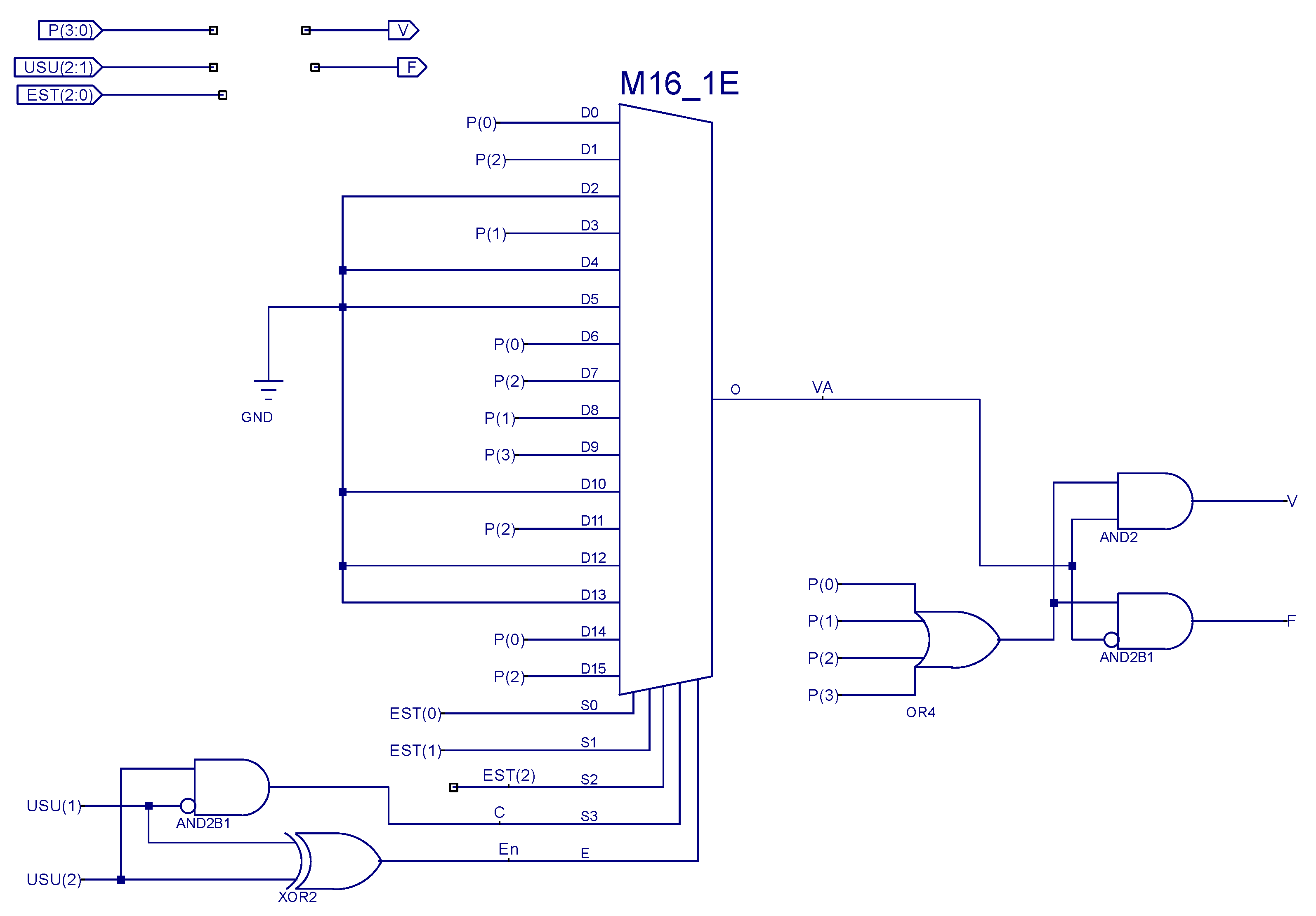
Figure 16 shows how the VCodAc combinational module was implemented in this project. Note that the enable and control signals in multiplexer M16_IE from the Xilinx library (E, and (S[3:0], respectively) come from the user selection signals (USU[1:0]) and the state of the control machine (EST[3:0]), while the mux inputs (D[15:0]) come from the pushbutton. Validation output signal V is therefore only active when the expected button is pressed in the corresponding state of the state machine.
Figure 17a provides a view of the system when an open sequence for user one is in progress. Door status is displayed in Nexys3. The four leftmost LEDs in the Nexys3 are all on while the word “CLOS” is shown in the display. We also know that two valid buttons of the open sequence were entered. This is because two of the three rightmost LEDs in the Nexys3 come on and a third is off, meaning the system is waiting for the third button of the sequence to be pressed. After pressing this third button, the door changes to open, “OPEn”, as shown in
Figure 17b.
The main tasks for students in this project (AccCtrl_RL) are to:
Design the control module in
Figure 15 as a finite-state machine based on the specifications provided in the practical training guide.
Verify the correct operation of the control module by simulating a given input sequence. This involves running simulations to observe the expected behavior of the door control system.
Incorporate the designed control module into the AccCtrl_LR project and verify system operation. Implement the complete design on the Nexys3 platform, and ensure that the door opens and closes automatically as intended.
Analyze the VCodAc module, understand how it works, and make the fewest possible modifications needed to change a user’s access code, e.g., to change the closing sequence for user two.
By completing these tasks, students will gain hands-on experience in designing finite-state machines (control module), verifying their functionality through simulations and implementing the whole control system on the Nexys3 platform to observe real-world operation.
4. Discussion
This section summarizes the main concepts and contents of the Digital Electronics subject that students should have experienced after completing each project described in this article. The main results of the opinion/satisfaction survey carried out on remote laboratory users are also presented and analyzed.
4.2. Opinion/Satisfaction Survey
The analysis below presents the main findings from a survey that focused on users’ opinions and satisfaction levels with the application and effectiveness of the remote laboratory during practical sessions in the subject over the past three academic years.
Table 1 presents the key data collected from the survey conducted among students to gather their opinions and feedback on usability and overall satisfaction over the three academic years (‘20/‘21, ‘21/‘22, and ‘22/‘23). The survey consisted of 15 questions organized into different sections. Its purpose was to evaluate performance of the tool, identify shortcomings or failures, and collect suggestions for potential improvements. The answers were collected using a Likert scale from 1 to 5. The data presented in
Table 1 provide an overview of the survey results and serve as a basis for further analysis.
First of all, a slight downward trend in the number of students enrolled (81, 79, and 72) and a difference in the number of students taking part in the practical sessions (58, 75, and 69) should be noted, mainly due to repeating students who already passed the practical sessions in previous years. In any case, the success rate for the practical sessions is high (82.8%, 74.7%, and 82.6%, respectively), with a slight drop in year ‘21/‘22. A decrease in the number and percentage of students taking part in the survey is also observed (55.2%, 48.2%, and 26.1%). However, most of them state that they used the remote laboratory tool. The decrease in participation, particularly in the last year, can be attributed to the timing of the survey, which was presented to students after the end of the academic term. Participation in previous editions was around 50%. As the survey was anonymous, it was not possible to determine if all of these students belonged to the group that passed the practical sessions.
A change in trend is observed in frequency of use. In ‘20/‘21, a quarter of respondents say they used the tool often, and a majority 65.6% from time to time, mainly to debug or validate the design before demonstrating its functionality to the teacher (28.1% and 37.5%, respectively). However, in ‘21/‘22 and ‘22/‘23, around half of the students state that they used the tool often (52.0% and 42.2%, respectively), with the other half answering from time to time, mainly to debug or validate the design (49.0% and 47.0%, respectively).
The average degree of satisfaction, considering the different aspects of use that are asked about, is high in the three academic years (4.43, 4.15, and 4.38, respectively). In general, students believe that it makes practical sessions easier (4.44, 4.40, and 4.50), and that the web user interface is intuitive (4.41, 4.30, and 4.50). This upward trend may be due to the improvements introduced in the new version of the tool made available to students in the academic year ‘22/‘23. They also express their satisfaction with the availability of the resource (4.19, 3.60, and 3.6). However, we believe that this decrease in the index reflects the increasing demand for use of the resource, which was not met despite increased availability in the new version. Finally, for this block of questions, students believe that there is a good similarity between online and on-campus experiences (4.31, 3.90, and 4.40, respectively).
As for the question of whether the tool could substitute (or even replace) the on-campus laboratory, opinion is not clearly defined in either direction (2.56, 3.00, and 2.60), although students do believe it complements on-campus practical training (4.69, 4.50, and 4.60).
Finally, they express a high degree of overall satisfaction with the remote laboratory tool (4.31, 4.00, and 4.40), which is in line with the increasing average degree of satisfaction.
Students suggested several improvements and requests, including extending the current 5-min connection time limit, as well as further enhancing the web interface and administrative functions. Most reported bugs were identified and corrected in the latest version of the application.
Work is currently underway to expand the number of peripheral elements available for the use of a hex keyboard and other communication interfaces. We are also working on including other FPGA-based development platforms other than Nexys3.
