1. Introduction
An underwater glider is a class of Autonomous Underwater Vehicle (AUV) that is guided by an operator in a boat through an umbilical cable or by a human pilot via satellite commands. Submarine gliders have multiple commercial and scientific applications. Like other instrumented equipment such as buoys, gliders are used to study the vulnerability of underwater ecosystems. Like other instrumented equipment such as buoys, gliders are used to study the vulnerability of underwater ecosystems caused by industrial, tourist, urban activity, or due to phenomena such as global warming [
1]. Submarine gliders can be used in different extraction and exploration missions, in applications for measuring water quality parameters, in the oil industry, oceanography, the study of plankton and fauna, among others where human intervention is dangerous or even impossible [
2,
3,
4,
5,
6,
7]. For this reason, underwater gliders are very important for monitoring the ocean and new technological developments are necessary to provide robustness to the glider [
8,
9].
The Gulf of Mexico Research Consortium (CIGoM) and other institutions in Mexico carried out a project to understand how the Gulf of Mexico is being exposed to oil exploitation [
10,
11]. Oil exploitation is one of the most polluting economic activities with critical importance but it carries risks; it can disrupt complex ecosystems and the environment of the region [
12]. CIGoM designs mitigation strategies in case of large-scale spills, and for worst case scenarios, evaluates the potential consequences of different oil leaks accidents. For this reason, CIGoM lines of action include the establishment of oceanographic, biogeochemical, and ecological variables. The CIGoM project consists of the development of an ocean and atmosphere monitoring system, using buoys, HF radars, underwater gliders, and remote sensing. In collaboration with the Center for Engineering and Industrial Development (CIDESI, Mexico), an underwater glider is being developed [
13]. The incorporation of oceanographic technologies in underwater gliders for systematic, directed, and autonomous sampling will allow monitoring of physical and biogeochemical variables in the Gulf of Mexico, and this allows a more effective prediction and early warning of disaster due to activities like oil exploitation [
14]. The development of a proprietary glider equips the technicians involved with knowledge about the design, maintenance, and commissioning of underwater gliders, which inherently proliferates and enables cost reduction in technology development.
Underwater gliders need several subsystems to operate correctly. Their operations include the monitoring of internal variables for glider safety, communication with the command center, GPS system, buoyancy system, energy storage, and oceanographic data collection [
15,
16,
17]. There are several states in the process of launching and capturing of a submarine glider: (a) The surface mode in which the systems are tested. (b) The recovery mode in which the glider sends a signal when emerging. (c) The calibration state in which the glider stores the adjustment values of its pitch, roll, and variable buoyancy system. (d) The diving and apogee states when the glider performs a sawtooth movement while capturing data from the marine ecosystem. During these states, a large volume of sensor data must be stored [
4,
18]. The data obtained from gliders are so important and expensive to obtain that it is recommended to assess and retrieve information at regular intervals to minimize the risk of data loss or to detect data collection problems [
19,
20].
The need for cheaper and more suitable storage systems for gliders is clear: submarine missions increasingly generate more information, and the development of specialized strategies or storage systems for this application is a necessity to reduce costs and ensure reliable data capture. The strategies are canalized in optimal samplings, capturing data according to the specific situation [
21]. Some gliders are teleoperated and use umbilical cords to avoid problems when transmitting large amounts of data [
22]. Other gliders [
8,
23,
24] use hard disk drives; however, they are expensive and complicated to interface with electronic subsystems. The most economical and accessible technology currently used by gliders [
5,
18,
25,
26] are SD cards; however, data storage errors cannot be controlled, and for marine applications where continuous storage is required, SD memory has random delays of more than 100 ms that can lead to loss of information [
27]. NAND Flash memory chips are an interesting alternative solution, as their cost/density ratio is increasingly lower, they allow total control of all their processes, and their error correction module is designed based on this application. However, there are further considerations for a glider, and a more in-depth analysis of the problems that may arise is necessary in order to define the software layers.
There are various layers and functions necessary for data storage in a glider: (a) The storage system for a glider must maintain information in the correct order for later reading. (b) The design, evaluation, and validation of a storage system represent a challenge for the operations of receiving, encoding, writing, reading, and erasing the information in a memory chip. (c) The data storage must be fail-safe in the event of loss of electrical energy; it must not store information in bad memory blocks, avoiding the corruption of information as a result of errors intrinsic to the storage system. (d) The sensor samples are taken from a master controller; however, it is important to have an efficient system for handling the data to be stored [
28]. For this reason, we propose a novel design comprising different layers of software integrated into a datalogger, which is a type of storage system that is composed of a storage unit and a processing system. The datalogger ensures that the information collected by the sensors connected to the master controller is correctly stored. The system considers the different failure modes mentioned above that could affect the data storage.
Before designing our datalogger, we carry out an analysis of the state of the art systems. There are several dataloggers, some for specific applications, others for general purposes. These have been used to validate prediction models based on environmental variables [
25,
29,
30]. They have also been used in civil structures [
31], livestock applications [
32], biomechanical applications [
33,
34], energy monitoring [
35], and for the internet of things [
36]. However, the aforementioned commercial and non-commercial data loggers do not have the characteristics mentioned in the previous paragraph which are necessary to manage the different failure modes that could damage storage in an underwater environment. In addition, a datalogger must adapt to different devices, so it must of a suitable weight and size for underwater gliders [
1,
37]. These reasons justify the development of a tailor-made datalogger for the specific glider application.
Our novel design, comprised of different layers of software integrated into a datalogger, uses a NAND flash memory chip, which is widely used due to its high speed in writing, reading, and erasing operations, and for its high storage density [
38,
39,
40]. However, NAND flash memory chips suffer wear and bit-flipping because their cells are highly dense [
41]. The writing/erasing operations degrade the NAND flash memory chip and increase the probability of bit-flipping. Error correction codes (ECC) are used to improve the reliability of NAND flash memory chips, reducing the probability of errors during their lifetime [
42,
43,
44]. In this paper, the ECC used is a BCH, which is one of the most recently used in flash memory and digital communications systems [
45,
46]. The BCH code used corrects 4 bad bits per 255-bit code. An indicator of memory chip degradation is the decoding time, it means that, an increase in the reading time of the information is a sign that the memory chip is beginning to wear. This article describes the hardware and the different layers of software of the datalogger for orderly and correct storage. The characteristics that are described are as follows:
Collection and storage of calibration variables and external signals monitored in different sections of the memory, and for different operating states of the underwater glider.
Method to choose and integrate the BCH module to the storage system and detection of bad blocks.
Integration of a failure protocol in the event of loss of electrical power.
Integration of NAND flash operations: read, write, and erase.
Section 2 describes the datalogger system in detail in terms of hardware design, software, choice of ECC, and read and write algorithms on the NAND flash memory chip.
Section 3 presents the obtained results for write, read, and ECC operations. The results confirm that the proposed design presents a good performance. In
Section 4, the discussion of this project is presented, and in
Section 5, the general conclusion is given.
2. Datalogger Design
To the datalogger design, first of all, we present the data to be stored as well as a brainstorm with the datalogger failure modes to design a software and hardware in order to reduce risks.
An ECC code to reduce error probability in bits is necessary, thus we present a design of the ECC that must operate in parallel with the data collection. Finally, reception, encoding, reading, and decoding are implemented in an MSP430 microcontroller based on state diagrams.
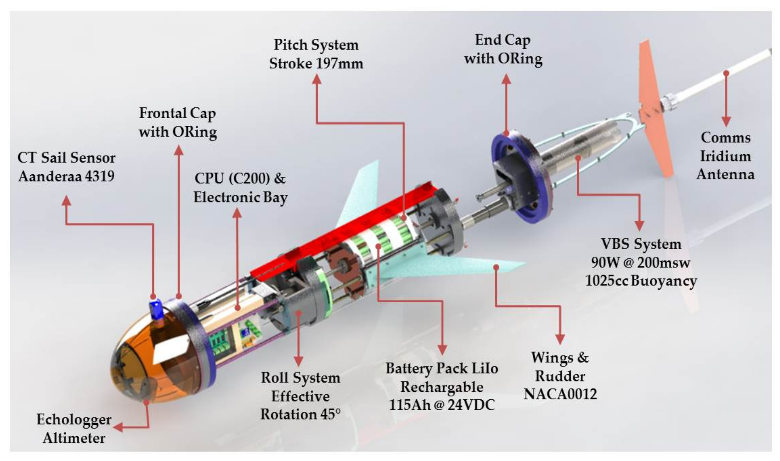
Multiple factors must be considered in the design of a data storage system: the type of memory device to be used, the sampling period, the type of error control intrinsic to the device, and controls against loss of electrical energy. The solutions that currently exist in storage devices may be suitable for different applications. However, an ad hoc device of a more suitable size, which facilitates the integration to a submarine glider is necessary. The glider developed in CIDESI is shown in
Figure 1. To perform further analysis, it is necessary to monitor multiple variables. Some of the variables that the glider must monitor and store in the datalogger are listed in
Table 1 There are 256 bytes that are obtained per sample, and 30 samples are taken every minute. In a later section, the storage period for different capacities of the memory chip will be described.
For the current time period requirements of the glider in development, the storage device was the Spansion S34ML08G NAND flash memory chip [
47]. It has a capacity of 1 GB and is reasonably accessible because pieces with this features are economic and easy to find in different electronic product suppliers. A summary of the device features of the NAND flash device is given in
Table 2. The chosen microcontroller is an MSP430 [
48] which has a DMA module that allows concurrency between data storage and reception. The characteristics of the chosen microcontroller are summarized in
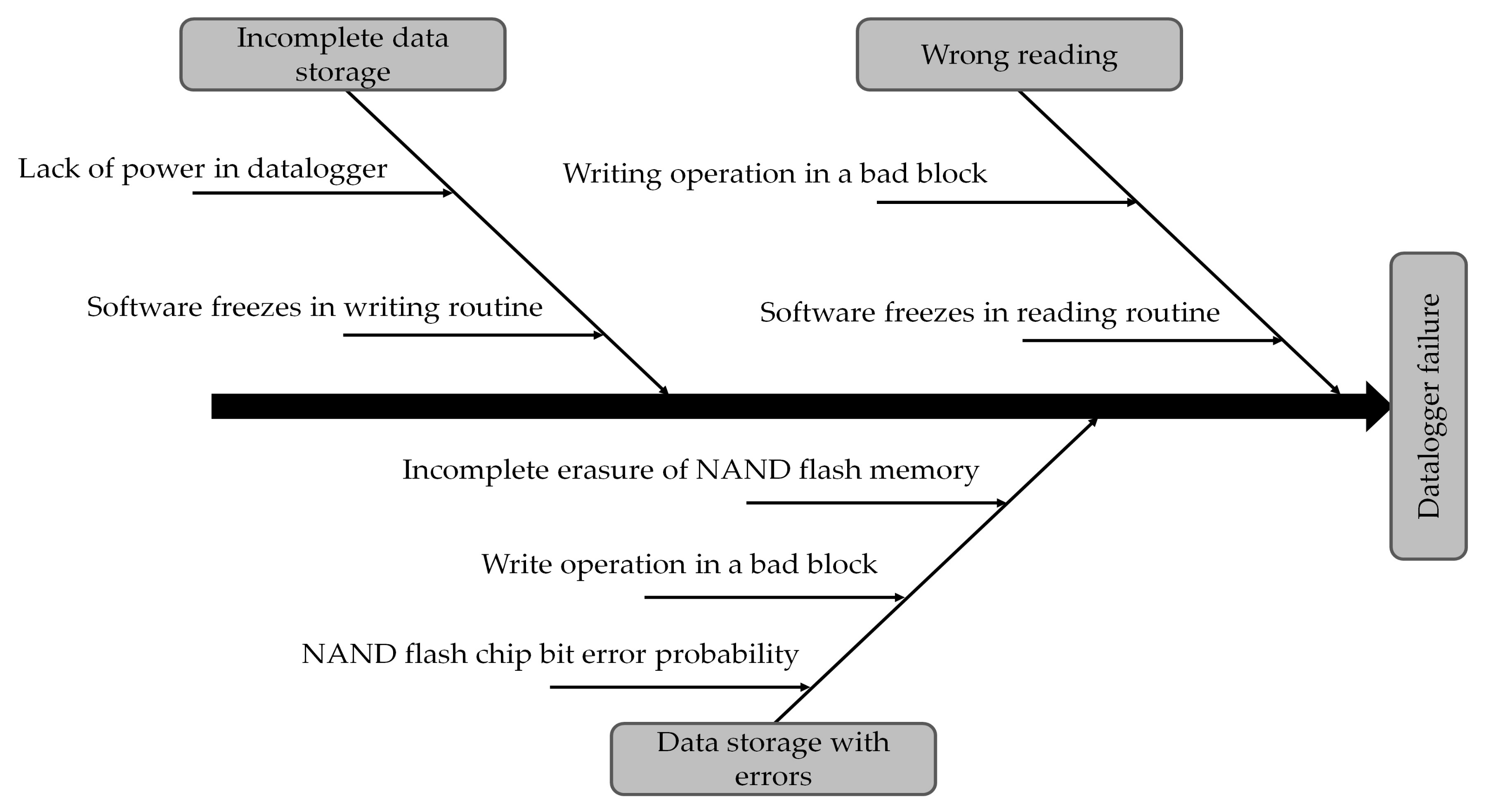
Table 3. The microcontroller performs the operations of writing, reading, erasing, and updating commands for the configuration of variables of the glider. Due to the different failure modes that can occur during the storage of the information generated by the underwater glider sensors, the possible causes were first mapped out (
Figure 2).
One cause of failure is due to the bit error rate, which is eliminated by implementing an ECC code, write operations out of bad blocks, and successful erasure operations. However, writing problems can also occur due to lack of power or code freezing at some point without exiting. Other type of error happens in the reading operation, it is important to make sure that the software does not get stuck at any point in the code.
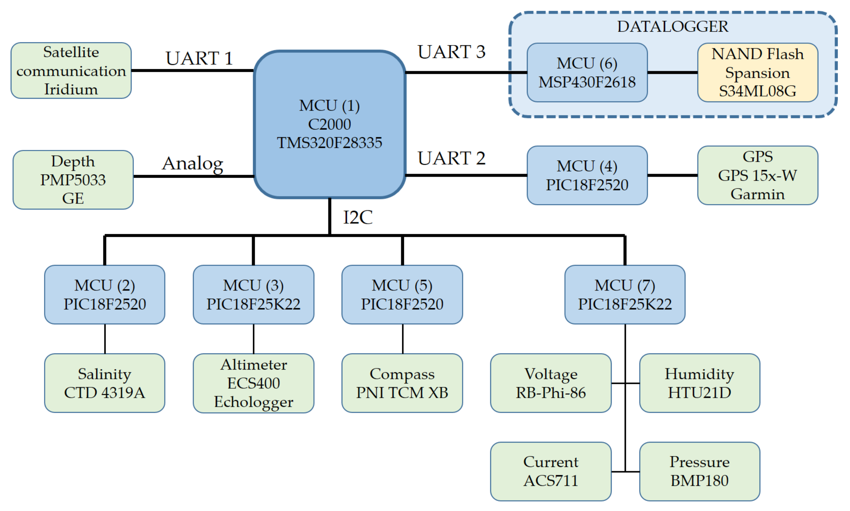
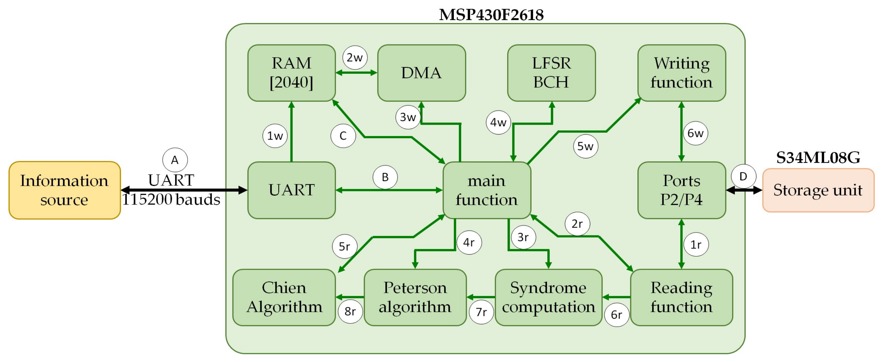
Figure 3 shows the connection diagram of the electronic system in the glider, and
Figure 4 shows the general block diagram of the datalogger. The central computer (C2000 microcontroller) sends information via serial bus at 115200 bauds (A and B) to the datalogger microcontroller. The MSP430 sends commands of configuration data, and commands to write, read, and erase the NAND flash memory chip. In the case that a write command is sent to NAND flash, then the datalogger activates the DMA (3w) and the DMA allocates the RAM (2w) to temporarily store the data that arrives via UART. The main function takes the data from RAM (C) to pass this data to the LFSR BCH (4w), and thus send it to the NAND flash memory chip through (5w, 6w, and D).
In the NAND flash read command, the microcontroller activates the Reading function (2r), then, the NAND flash memory chip is read (1r and D). The data received is transferred to the syndrome computation function (3r and 6r). Then, the error locator polynomial is searched through the Peterson algorithm (7r) function [
49], and then the roots are calculated with the Chien Algorithm function (8r) that returns the positions of the errors [
44,
49]. With the positions of the errors, it is possible to correct corrupted bits of the NAND flash memory chip in order to send them to the data source via UART at 115200 baud (B and A).
2.1. Study and Choice of the ECC
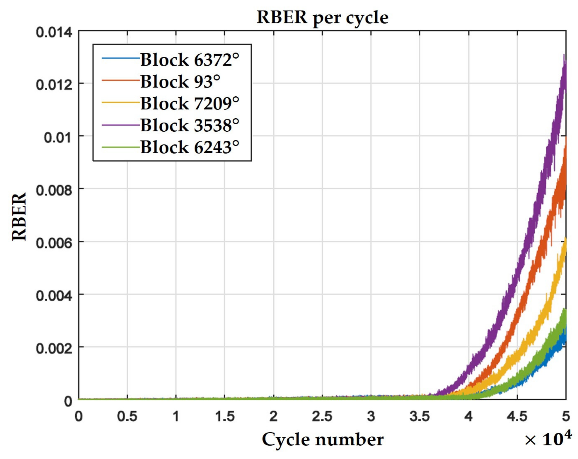
The storage device has two types of errors. The first one is due to the cells of the NAND flash memory chip are densely populated, and generate bit-flipping errors.
Figure 5 shows the behavior in the degradation of the NAND flash blocks. To reduce this bit error rate (BER), the storage device must have an error correction code. The second error is due to the existence of bad blocks. A bad block is a block where data cannot be written or erased. The way to detect bad blocks is by reading the first byte of the spare area of the first page in each block [
50]. In the case that the first page would have a bad block mark (00 h), then, a table of bad blocks must be updated and stored in a flash section of the microcontroller. This operation must be performed during the first time that the NAND flash device is used. If a block is erased, the bad block marks are also erased.
The NAND flash device used has an ECC embedded that corrects 1 bit for every 528 bytes. However, the ECC embedded is not enough to avoid all errors, and the datalogger could host other storage devices that do not contain embedded ECC. In addition, including an ECC increases the correction capability and therefore it is possible in this case to have a NAND flash memory chip reliability up to a of , that is, approximately 3 devices out of 100 will have at least one erroneous bit.
In order to determine the code length and the corresponding correction capabilities of the BCH code, it was necessary to characterize all error features that are present in the NAND flash memory chip. According to the authors of [
51,
52], the most common errors found in a NAND flash memory chip are random; however, erroneous bits are independently distributed, so the errors can be modeled as a Bernoulli process [
53], with the following properties:
The experiment is based on repeated runs, each run consist of visualizing whether blocks composed of BCH codes of length n have errors.
For each bit, there are two types of results, i.e., defective and non-defective.
The number of successful runs must be similar at each run. In other words, the error in bits are independent events.
The goal is to find a BCH code
capable of achieve a low bit error probability, implementable in the microcontroller, that the data of interest (message) occupies most of the NAND flash memory chip. The parameter
n is the code size,
k is the message size, and
t is the correction capability. The formula of the binomial distribution applied to the NAND Flash memory chip model [
44,
53] is represented in the following equation:
The above equation
represents the probability that there are i errors within a BCH
code of length
n.
p is the error probability also known as raw bit error rate (RBER) before using ECC. When there are more than
t errors in a code, then the correction can be considered failed. Then, the failure probability
b in a block code of
n bits to which the ECC that corrects
t errors applied is
The probability of error in the
NAND flash device with
B blocks of
n bits can be approximated with
To propose the code and message length of the BCH code, a natural number
m is used to meet the constraint
. To do so, there exist a number of binary BCH codes with a correction capability of
, and
parity bits [
54]. With these parameters, the analysis was performed for some BCH codes with
and
, that is, of lengths
bits and
bits. For example, for the arrangement BCH (255, 223, 4) that corrects 4 errors per 255 bits at each code, and using a NAND flash memory chip with a storage capability of 4,194,304 codes of 255 bits each one, with an RBER of
p = 2.36 ×
, so the probability for
i errors in a code of 255 bits is computed by Equation (
4), where
i is the interval
, in which each number indicates the correction capability.
where
i can take the values from 0 to 4 which is the correction capability. The expression that indicates the fraction of devices that may have an error is
In the case that the type of error was another type, for example, bursts, then the type of model is not binomial and the previous expression would not represent a good approximation. In our case, it is used, as NAND flash memories present random errors, so it can be modeled in the form of Bernoulli process [
44,
53].
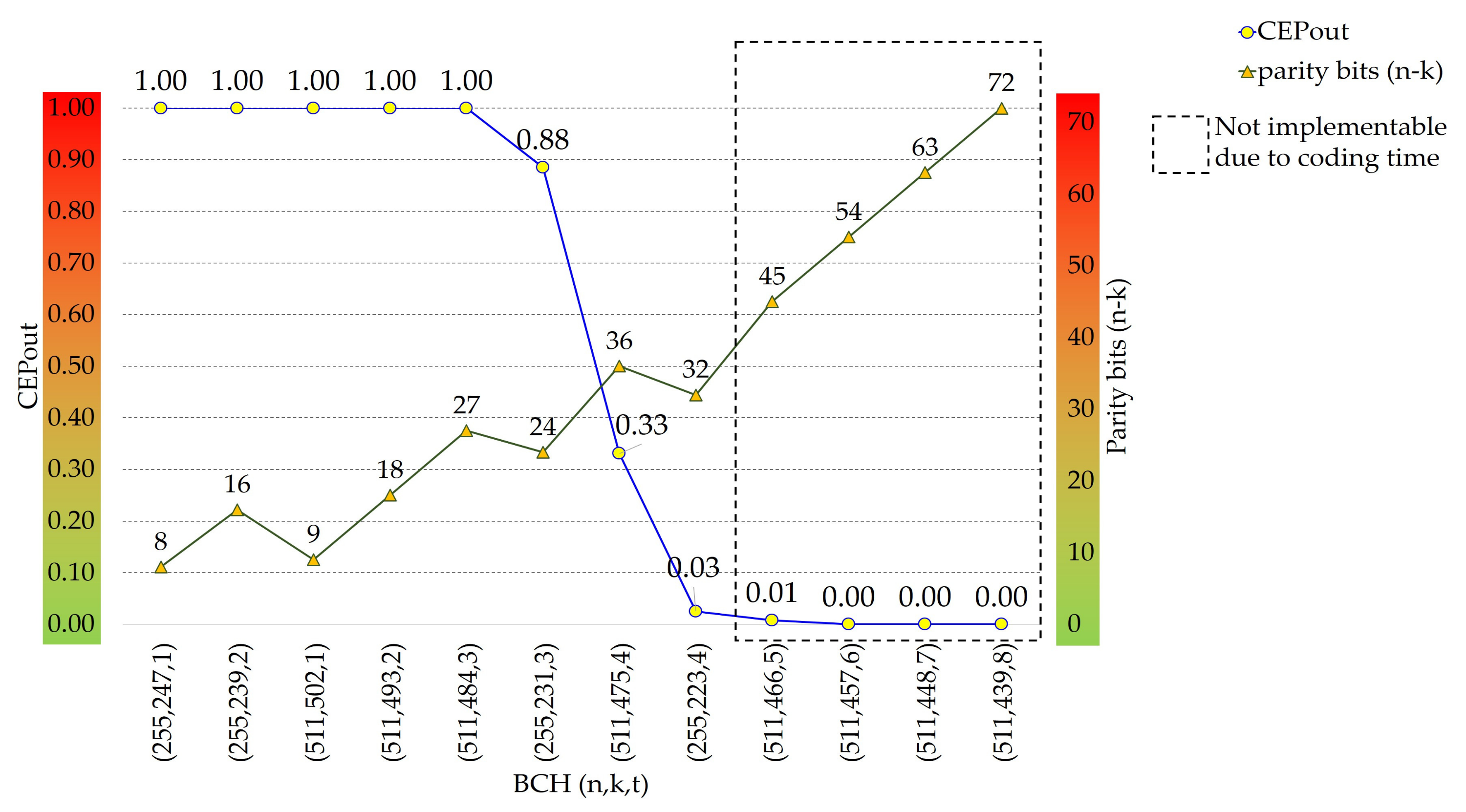
Figure 4 shows a comparative graph of different BCH codes of code length
and
and with different correction capabilities. The left vertical axis represents the probability of error in the NAND flash device after performing error correction. The right vertical axis represents the added parity bits. When more parity bits are added, the correction capability increases, however, the data rate
also decreases, that is, less representative data is transmitted in a sent code. The data rate is also an indicator of how much area of NAND flash memory chip is used for parity bits. The number of parity bits is an indicator of how long it may take for the microcontroller to perform the BCH encoding. In
Figure 4, it can be seen that as the correction capability of the BCH increases, the probability of error in the device also decreases and the added parity bits increase.
The code chosen was a BCH (255, 223, 4). In
Figure 6, it can be seen that to the right of the BCH code (255, 223, 4) there are other codes that may have a higher correction capability; however, the data rate is also lower. With the chosen BCH code, the data rate
is
.
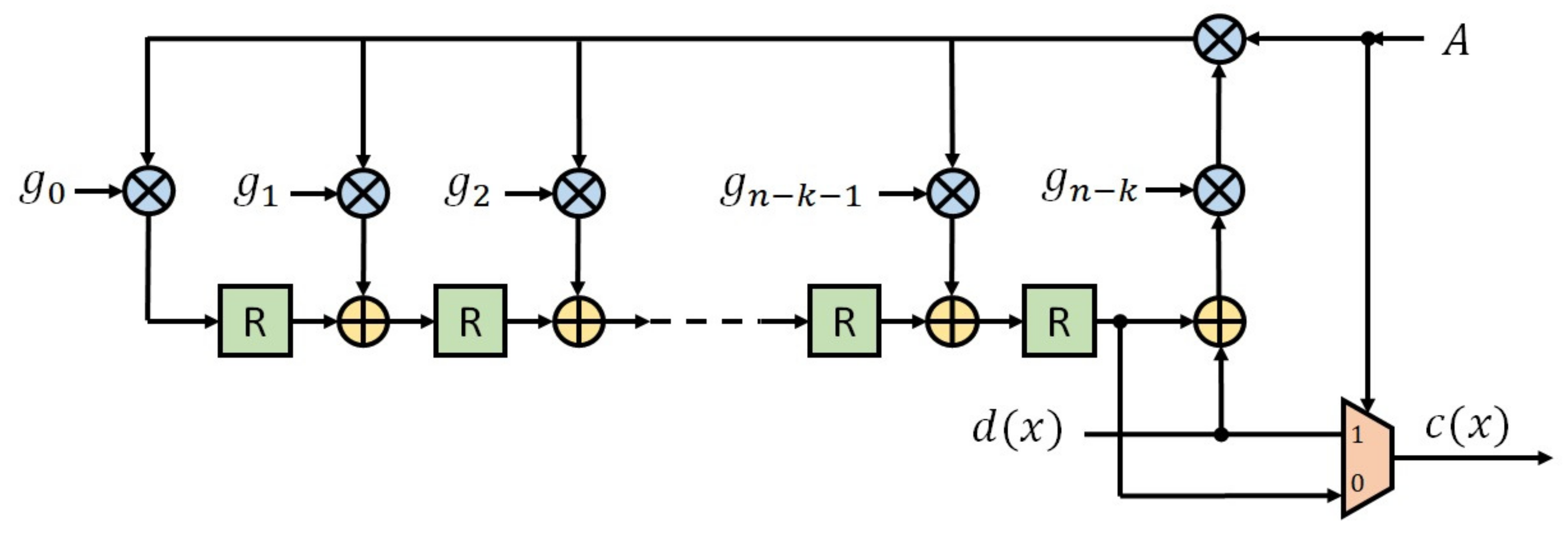
BCH encoding is performed using the LFSR of
Figure 6, in which it can be seen that there are AND and XOR operations, shift registers, and a multiplexer [
49]. The real form of the LFSR and the operations to be carried out depend on the parameters
n,
k, and
t of the BCH code and on a generator polynomial that is mentioned in the next section.
2.2. LFSR Development for the BCH Code (255, 223, 4)
An ECC code is composed of message bits and parity bits. For a BCH code, systematic coding is done using the Equation (
6).
where
represents the message,
the added parity bits,
n the length of the code,
k the length of the message, and
the code. The parity bits
are obtained by modulo operation as presented in the Equation (
7):
where
is the polynomial generator of the BCH code, which can be obtained with the MATLAB
TM function bchgenpoly. This function requires the length of the code and the length of the message. The generator polynomial given by the function is the following:
To obtain the parity bits, a systematic LFSR cyclic code encoder circuit is used as shown in
Figure 5, where
is the coefficient of the second term with the highest exponent of the generator polynomial and always takes the value of 1 as well as
.
The way the LFSR circuit in
Figure 7 encodes is described below.
- 1
The shift registers R must be initialized with the 0 value.
- 2
During the initial k cycles, the term A is defined with the 1 value. The value taken by the multiplexer is defined with the 1 value, and the most significant bit of the datum is shifted into the LFSR first. The input in this state are the 223 message bits and the output takes the message bits.
- 3
For the last
cycles,
A has the 0 value. That means, the values in the multiplexer are used in the most-right register which are the parity bits. In this research work, the registers
R are deleted at the end. Each bit that goes through the multiplexer is concatenated with the previous one. In other words, at the end of each cycle, the code is constructed from the message and 32 parity bits [
49].
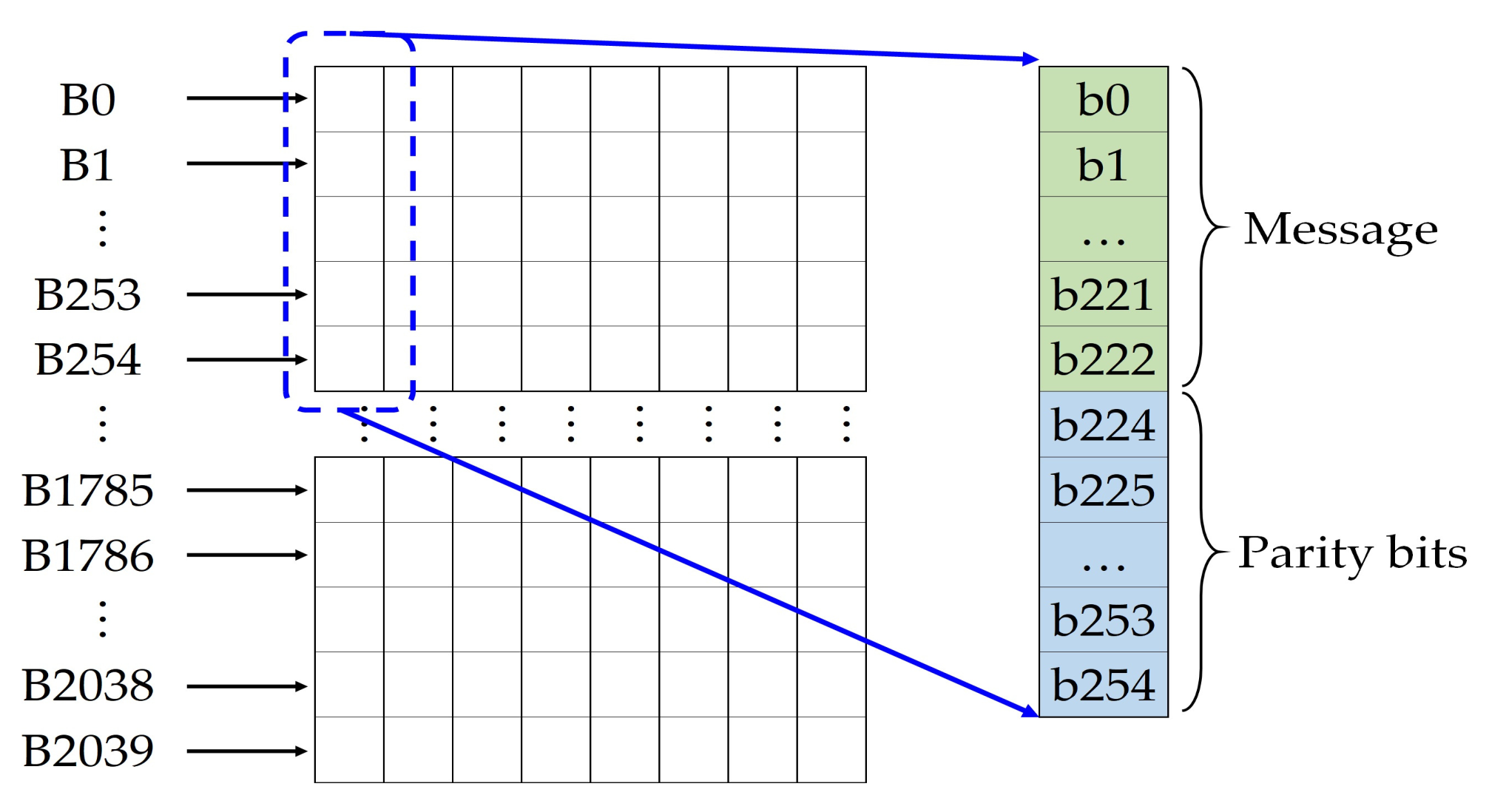
Writing on a page of the NAND flash chip was performed in portrait orientation as shown in
Figure 8. The reason it is available this way is because it takes advantage of the logical operations of the LFSR. In the next section, writing on the NAND flash memory chip is described.
2.3. Data Writing
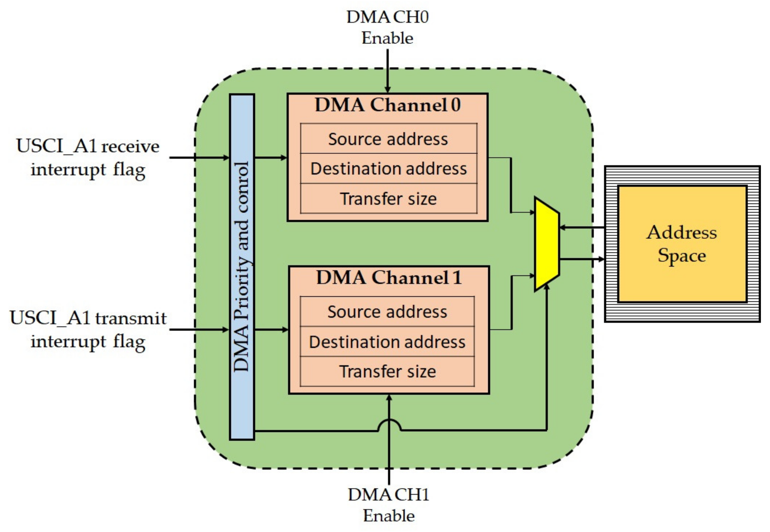
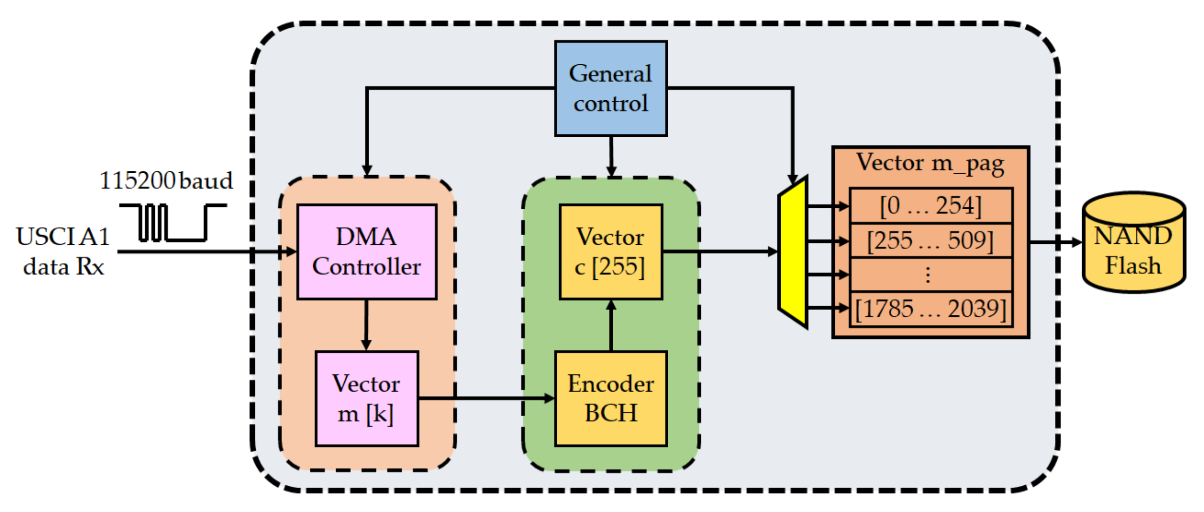
For the writing operation is required to send a command to the datalogger in order to perform the desired operation. To perform a write in a page is necessary to erase the block’s page. The erase operation is done out of the water when there is no more storage space. The erase time is not considered in the average performance because the memory chip is erased before the glider is submerged, then it is only written to NAND flash in which there will be no erase operations. In order for all data received by serial to be stored in the NAND flash memory chip, data encoding and writing operations in NAND flash must be performed in parallel with serial data reception. To achieve this, the DMA module is used for serial reception.
Figure 9 shows the general DMA module diagram. There are three DMA channels. Initially, the datalogger used two modules: one for reception and the other for serial transmission. However, the bottleneck in reading NAND flash is decoding, and therefore we do not occupy DMA in serial transmission. Each DMA channel has three registers: the source address, the destination address, and the transfer size. For DMA channel 1, the source address is the serial UART RX buffer, the destination address is a vector where a message of k bytes is temporarily stored, which is the transfer size.
The block diagram for the write protocol of the NAND flash unit is described in
Figure 10. Concurrent operations are performed, the CPU controls the send of commands to NAND flash for writing, reading, and erasing operations. In the other hand, the DMA performs serial reception. In
Figure 10, the source address of the DMA is the RX buffer and all data that are received by serial bus through the vector
m of
k bytes. At the same time, the BCH encoder adds parity bits to vector
m, the message and parity bytes are temporarily stored in a 255-byte vector
c so that they are then stored in the
vector that corresponds to a complete page of 2040 bytes. Then, data are stored in a NAND Flash memory page.
To write to the NAND flash memory chip first of all, the pointer that contains the last write address must be read. In case it is the first write operation, the pointer should be in the logical zero write address. In case there has been any loss of electrical power, the write address should have been updated during the last write cycle. After reading the pointer, the messages are received by the microcontroller by serial at 115200 baud. In order to receive the data and concurrently perform the encoding and writing in NAND Flash, the Direct Memory Access DMA module is required. Two states were used to activate channel 1 of the DMA: and . These states are for the microcontroller to perform the function of activating channel 1 of the DMA, which has as its source a UART RX buffer, as its destination a message vector m and a size transfer of 223 bytes.
For the underwater glider, there are two different write operations. The first operation is the configuration data of the glider, which are stored on the first page of the first block of NAND flash memory chip. The other write operation corresponds to the storage of variables provided by mission. Metadata and regression coefficients that may be required for future maintenance of the submarine glider are also stored. In case the potential power loss failure occurs, a record of the last write address is kept stored in the flash memory chip of the microcontroller and from this address, writing is started each time the datalogger is used. When the microcontroller turns on, the first thing that is done is to read a pointer with the last writing address of the NAND flash memory chip. This block address is assigned to a location in the flash memory of the microcontroller. Each time a complete block is written, the flash memory location updates the last block written.
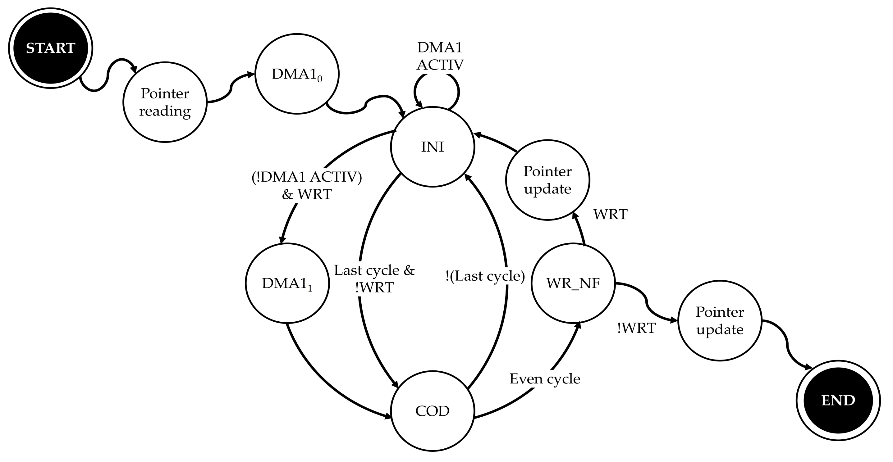
The writing operation begins when the datalogger receives a write command via serial bus. The writing process is visualized in the state diagram of
Figure 11. The write operation begins by reading the pointer that contains the last physical address written to NAND flash memory. Then, the
state which activates channel 1 of the DMA to receive 223 bytes of message via serial UART. Then, it goes to the INI state and remains there as long as channel 1 of the DMA is active. Then, it goes to the
state that activates channel 1 of the DMA again and immediately goes to the COD state which encodes the
-bit vector that was acquired by the DMA, at this time, both the encoding and the data reception are executed in parallel. To avoid overwriting information due a power failure, a pointer indicator of the last page and last block written is updated in the Pointer state. In this way, in case of power loss, the previously stored information is not corrupted. Then, it returns to the INI state which again waits for channel 1 of the DMA to be inactive. The iterations continue until the last cycle is reached, in which the last bytes are received, which, once the information is encoded, fills a page of NAND Flash memory chip. After the NAND flash memory is written, the last written address pointer is updated.
To continue writing in the NAND flash memory the WRT signal is needed. In the case of continuing writing, it re-activates channel 1 of the DMA to receive, encode, and finally write to the NAND Flash memory. In the case that the period of time in the falling and rising edge of R/B# could be fast, the microcontroller could cycle waiting for the falling edge of R/B#. Therefore, a step is not put to wait for that fallinf edge. Instead, the result of the 0x70 command is awaited; thus, the microcontroller does not remain cycled. In the case of not continuing to write, then it goes directly to the COD state to encode, then to the WR_NF state to write in NAND Flash and the writing process is finished.
2.4. Data Read
For data reading, DMA was not used as the decoding time was higher than the data reading time, so the operations of reading and decoding a NAND flash page cannot be performed on the microcontroller concurrently. In the case of reading NAND flash memory, the bottleneck is decoding and there is no significant improvement between using DMA or not using it. However, the reading process is not critical except that as in writing, a falling edge of R/B# event occurs and can be very fast. Instead of waiting for the falling edge and then the rising edge of R/B#, a delay time is placed. This prevents the microcontroller from waiting for the falling edge of R/B#. The data read from the NAND Flash memory are temporarily stored in a vector R, which contains the codes stored by the encoder: message and parity bits. Once the memory chip is read and the R vector of 2040 bytes (8 × 255 bytes) is filled, the decoding composed of the following:
- 1
Syndrome computation.
- 2
Computing of the coefficients of the error locator polynomial.
- 3
Finding roots and reciprocals of the error locator polynomial.
With the consequence of the reciprocals of the error locator polynomial, the error vector is obtained, where the erroneous positions take a value of logic one ‘1’ in the coefficients of the error vector. The error vector is represented as the polynomial:
Then, the XOR operation between vector
e and
R is performed to obtain the
vector that contains the decoding of the vector received from the NAND flash memory chip. In case the error correction capability is greater than the added errors, which in our case are a maximum of 4 errors, then the
vector will be the same as
, which is the code written in the NAND flash memory chip. As can be seen in
Figure 12, the 2040-byte
code is processed and the parity bits are removed. Then, the transmission consists on send 1784 (8 × 223) bytes. These data are of interest to the user: the message.
The syndrome calculation is the very first step to perform the decoding process which involves replacing the value
in the polynomial expression
.
are elements of the
generated by a primitive polynomial
. The replacement is
where
, for our case,
, having eight elements for the syndrome
. To determine the coefficients
of the error locator polynomial
, a Peterson’s algorithm with a correction of
is used, the equation to solve is
that can also be written as follows:
Once the coefficients of the error locator polynomial are determined, its associated roots are now estimated. Therefore, the found polynomial is
To calculate each root,
x is substituted by the value of the Galois-extended-field roots. This process is implemented to find all roots is the Chien algorithm where each value
x is substituted in the error locator polynomial. The values of
x that are substituted are
When
is obtained to the substitution of the every element of the extensive Galois field, then that element is a root. After finding the roots, the reciprocals of each of the roots are obtained, these inverses indicate the error positions. Each of these error positions generates the error pattern polynomial that is added to the received word
to obtain the code
. In the case that correction capability was greater than the number of errors,
represents the code stored in the NAND flash memory chip.
3. Results
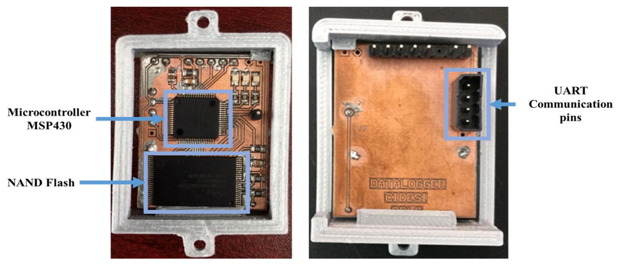
The printed circuit board for the datalogger is illustrated in
Figure 13 which shows the components such as the microcontroller, the NAND flash memory unit, and the communication ports. We performed three tests to validate the correct operation of the datalogger. The first test corresponded to the writing of the NAND flash memory chip. The second test was for reading the NAND flash memory chip simulating up to 4 errors for every 255 bits of code. The third test was for the power consumption of the datalogger. Finally, we describe a final test in a sea mission.
The NAND flash writing test is very important because the storage of all data depends on it. The sum of encoding and writing times in NAND flash must be less than the reception of serial data. The second test for reading NAND flash with four errors has the target of knowing the time it takes to perform this operation in the case of the largest possible number of errors to be corrected by code. In the third test, 1, 2, 3, and 4 errors per code were added to corroborate the correction capability, to know the behavior of the decoding time by number of errors, and to find a relationship between the number of errors and the decoding time, and thereby obtain a characterization.
3.1. Results for the Writing of the NAND Flash Unit
The data transmission from the sensor monitoring system sends an average of 128 B/s. If the transmissions were to be carried out at 1280 baud, which would be the minimum transmission speed to be able to perform lossless storage, then the microcontroller would remain working for the entire period of time. That is why the transmission is done at a standard speed of 115200 baud, so that the microcontroller has long waiting periods. This allows to use the low power mode (LPM) that is activated while the DMA is waiting for data by UART.
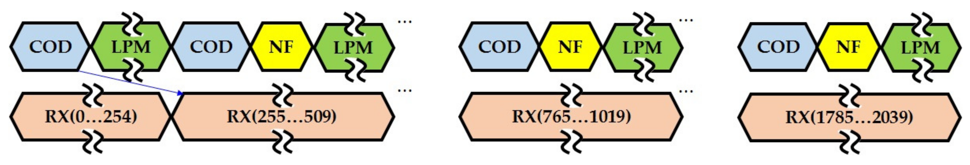
To find out the behavior of the datalogger in a limit situation, the transmission speed was 115200 baud and without breaks. For the write process that is related to the NAND flash memory chip with serial data transmission, the state diagram was presented in
Figure 11. The process of data writing in the NAND flash unit was carried out every 255 bytes, therefore a random write process for the NAND flash memory unit is employed. The first random write was realized on the address columns that are defined in the interval 0–254. The second random write process was defined in the interval 255–509, while the third random write goes from 510 to 764 and so on until the last write goes from 1785 to 2039.
The DMA UART receive operation was performed in parallel with the encoding operations, writing to NAND flash, writing the last page accessed from NAND flash, and waiting for the next command. In order for the information to be stored without loss, the period time of the operations performed by the CPU is required to be less than the RX data reception operation performed by the DMA module. The mean of the time periods in the operations were obtained, and the summary of times for NAND flash writing taking the data by serial at 115200 baud is presented in
Table 4 and in
Figure 14. It can be seen that
Where is the encoding time by the BCH code, is the time for the basic sequence of NAND flash writing operation, is the period of time to storage the address of the last page accessed, and is a timeout of the data by the UART receiving port. The sum , , and must be less than the reception time by UART . The period of time for writing in the memory flash of the microcontroller is μs and represents a very small period of time compared to the times , , and .
There is a Low-Power Mode time
in which the microcontroller sleeps until an interruption UART is performed. In
Figure 14, it can be seen that every time 255 bytes are joined, a partial writing of the NAND Flash page is performed. The partial writing had to be done because if it was sent in a single 2040 packet, the sum
would be greater than
and it would not store in real-time.
3.2. Results for the Reading of the NAND Flash Unit
The second test corresponding to reading the data was performed for 115200 baud rate. The reading was done by mutating four bits per code in order to analyze the time for maximum correction capability. The sum of the memory reading and decoding times is higher than transmission, however the parallelism in the read operations is not critical as the read operation is performed after the glider operation (see
Table 5).
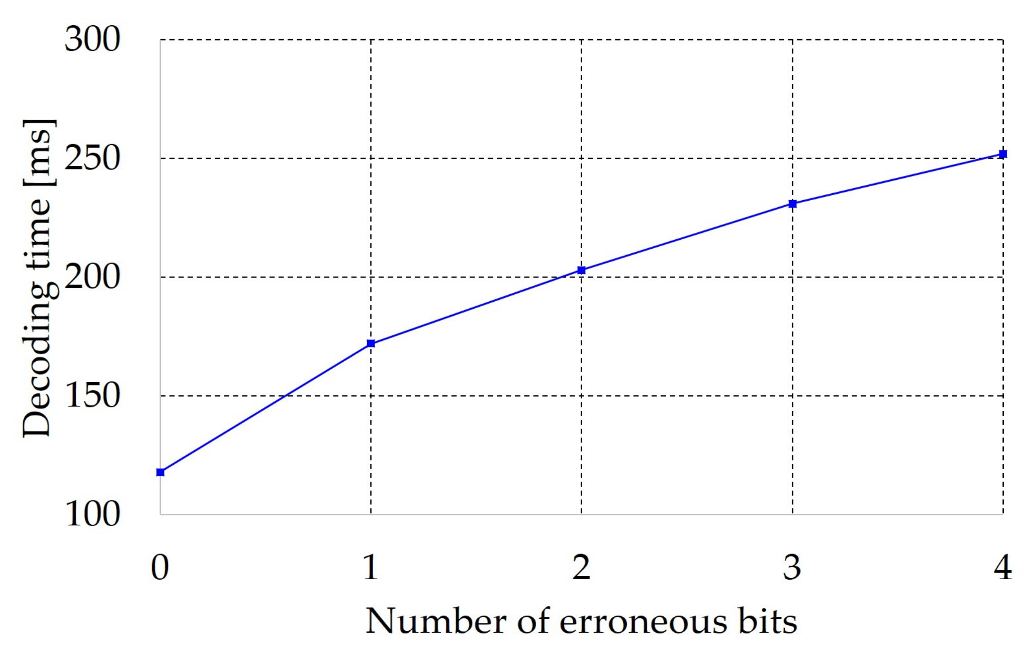
To test the BCH error correcting code, 0, 1, 2, 3, and 4 errors were added. The tests were performed in a way that there was exactly the same amount of errors in each code, with this, a homogeneous result would be obtained for a certain amount of errors, and with it, the decoding time in a certain correction capability. The result of reading the data decoding by BCH can be seen in
Figure 15. It can be seen that as the errors increase, the decoding time also increases. It can be seen that the decoding time is proportional to the number of errors corrected. The decoding time increases because more operations are required to find the errors.
3.3. Datalogger Consumption
To test the power consumption of the datalogger, the electrical current consumption was monitored for a write operation of the NAND flash memory chip in a flight mode operation. The power consumption of the datalogger during the information storage operation, and taking the data via serial at 115200 baud, is 1.6 mW. It means that if we use two batteries in series of 1.5 V and 3000 mAh each one, you would occupy the datalogger for more than 7 months.
Regarding the consumption of microcontroller resources, the consumption of the microcontroller can be viewed in
Table 6. The percentage of use of RAM and FLASH of the microcontroller is quite low. The resource still available can be used for other functions, for example, to restore values that are in flash and these are required to restore the datalogger to some original value, bad block addresses, wear leveling algorithms such as garbage collection, etc.
3.4. Final Test in Sea Mission
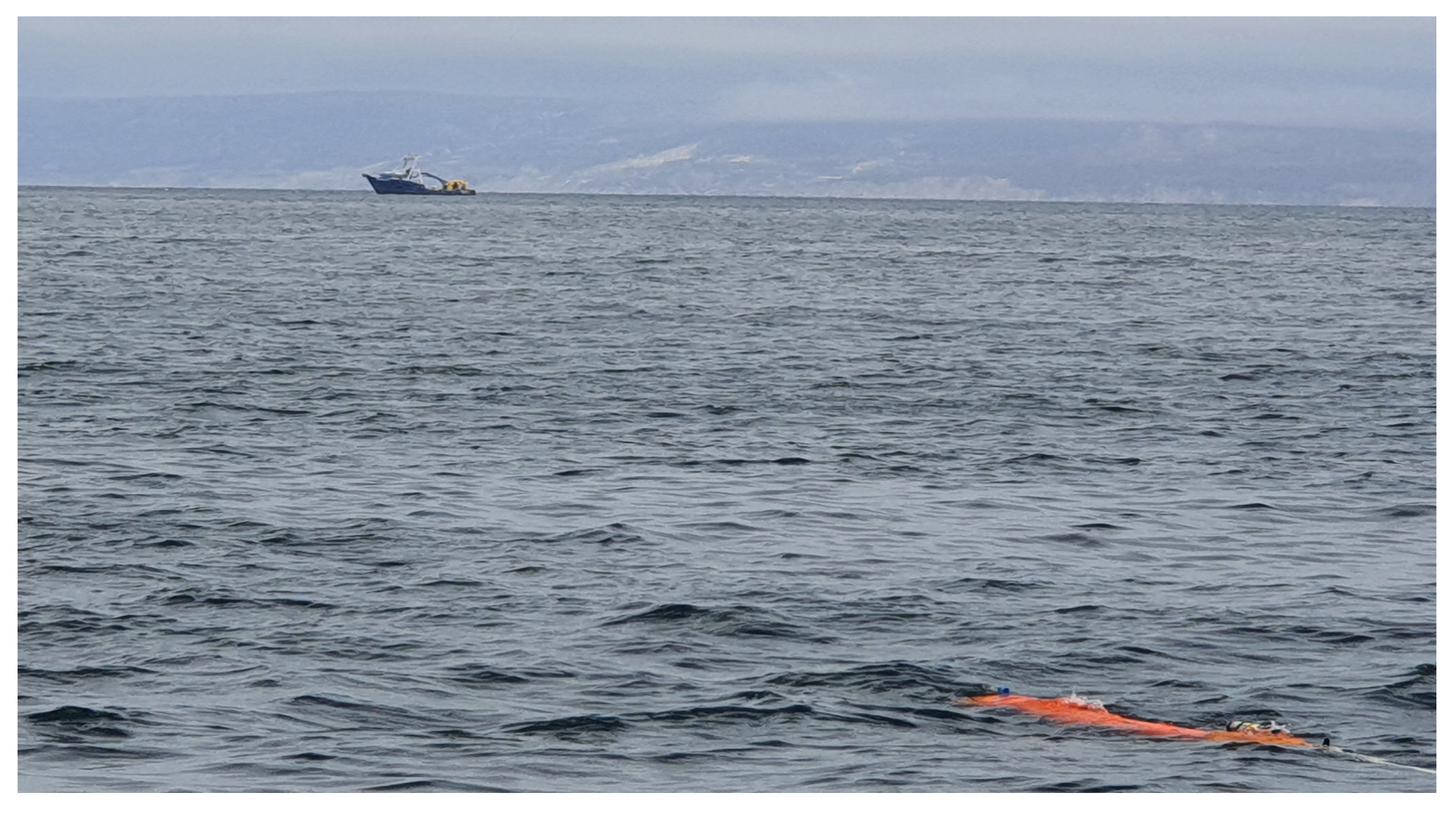
We carried out a first test of our glider at sea, specifically in the Bay of Todos Santos in Ensenada, Baja California, Mexico.
Figure 16 shows the glider emerging from the depths of the sea. Seven successful tests were carried out at a depth of up to 50 m. However, in the last test, the glider antenna did not withstand the pressure of 50 m. Therefore, the tests at that depth were concluded. The test allowed us to obtain important information about the glider operation, to be able to improve it. The operation of the datalogger went as expected during the mission.
4. Discussion
Submarine gliders have several systems such as buoyancy engine, internal and oceanographic variables system, and others. The integration of the system sensors generates a large volume of data. Our design points carrying out the different glider operation stages with a dedicated storage system are necessary. Moreover, our datalogger facilitates the storage operation avoiding data lost. For the design of the storage system software, it is necessary to take into account the different failure modes in order for the system to be robust. Faced with different failure modes, the developed datalogger has the following characteristics that gave satisfactory storage support:
The BCH module that correct 4 errors for every 255 bits functions without data lost due to it functioning in parallel to the data collection and because the ECC avoids the error in the CHIP with a of .
A layer to detect bad blocks that avoids the writing or erasing in blocks that could not be useful.
A protocol that updates an addressing writing pointer every writing operation. In a power loss event, writing starts at the last address.
Even with these characteristics, it is possible to identify, not necessarily disadvantages, but some limitations for the datalogger that are described below. Due to the vertical arrangement of the messages, the size of 2112 bytes of a page (2048 of data area and 64 of spare area), and because the length of an ECC code is 255 bit, the number of codes that could enter a page is . Therefore, the number of bytes of data on a page is . The fraction of the page that can be used for data is , that is to say, 87%. The fact that ECC codes and page size are power of 2 numbers does not necessarily mean that the efficiency of use of the entire page is 100%. However, the 87% represents a high usage percentage of a page memory chip and the ECC avoids the errors in data storage.
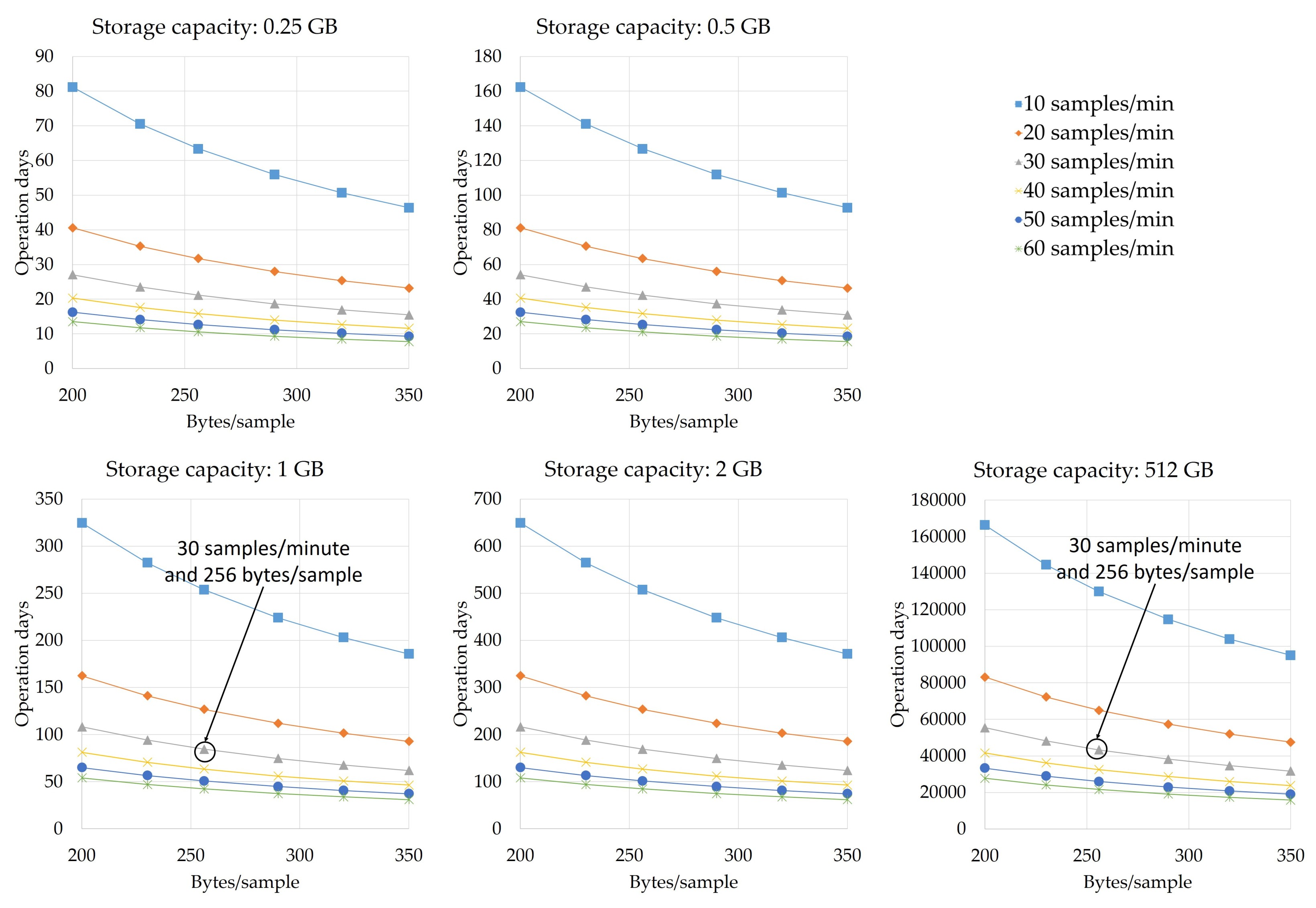
The maximum storage period is also limited by the sample rate, sample length, and the memory capacity used. For a sample rate
f in samples/minute, a sample length
L in bytes and a memory chip storage capacity
C in
, the period in days that can be store is
Figure 17 shows the maximum period time in days of the limit for different storage capacities of the chosen chip. For our case using 1GB NAND flash, a sample rate of 30 samples per minute and 256 bytes per sample, the time limit is 84 days. The graph in
Figure 17 shows us that if we use an storage capacity of 512 GB, you could use the datalogger for more than 40,000 days. It points that you can increase the sampling velocity or even the sampling size.
Other results indicate that one bit per
bits will be wrong. This number represents the uncorrectable bit error rate (UBER). At the memory chip level, there would be 3 bad chips for every 100 chips. Is important to say that a bad chip is one that has at least one wrong bit. When NAND flash memory begins to degrade, the probability of errors increases and more correction capacity is required. However, the degradation time will not occur for practical purposes. An analysis of
Figure 15 indicates that it is possible to predict the moment when memory begins to degrade. If the number of errors increases, then the decoding and the reading times increase too. One cycle of operation is when the datalogger erases a NAND flash memory chip block, and, next, it writes data on one page of this block. Thus, the degradation process of the NAND flash memory chip starts with many cycles of write and erase operations. The MLC-type NAND flash memory chips have 2 bits per cell, and the degradation process starts up to around 3000 read and write cycles.
The number of bits that must be added to a NAND flash memory chip reduces the life of the device; that is, it degrades it more quickly. For most memory chips discussed in
Figure 17, the minimum ECC required for data protection is approximately 40 bits per 1117 bytes. Our datalogger adds 32 bits for every 255 bytes. However, this relation is adequate for practical purposes because the underwater glider will not reach 3000 write and erase cycles during its useful life.


 ,
, 


