


Research on a DC–DC Converter and Its Advanced Control Strategy Applied to the Integrated Energy System of Marine Breeding Platforms


Abstract
1. Introduction
2. Bidirectional High-Gain Cuk Converter
2.1. Topology of Circuit
2.2. Operating Principle of the Converter
2.2.1. Step-Up Mode
2.2.2. Step-Down Mode
2.3. Steady-State Characterization
2.3.1. Voltage Gain
- Step-up mode
- 2.
- Step-down mode
2.3.2. Zero Ripple Characteristics
- Step-up mode
- 2.
- Step-down mode
2.3.3. Voltage Stress of the Power Device
- Step-up mode
- 2.
- Step-down mode
2.3.4. Characteristic Comparison
3. Passivity-Based Control with LADRC
3.1. Design of the Passive Controller
3.2. Design of LADRC

4. Results
4.1. Simulation Results
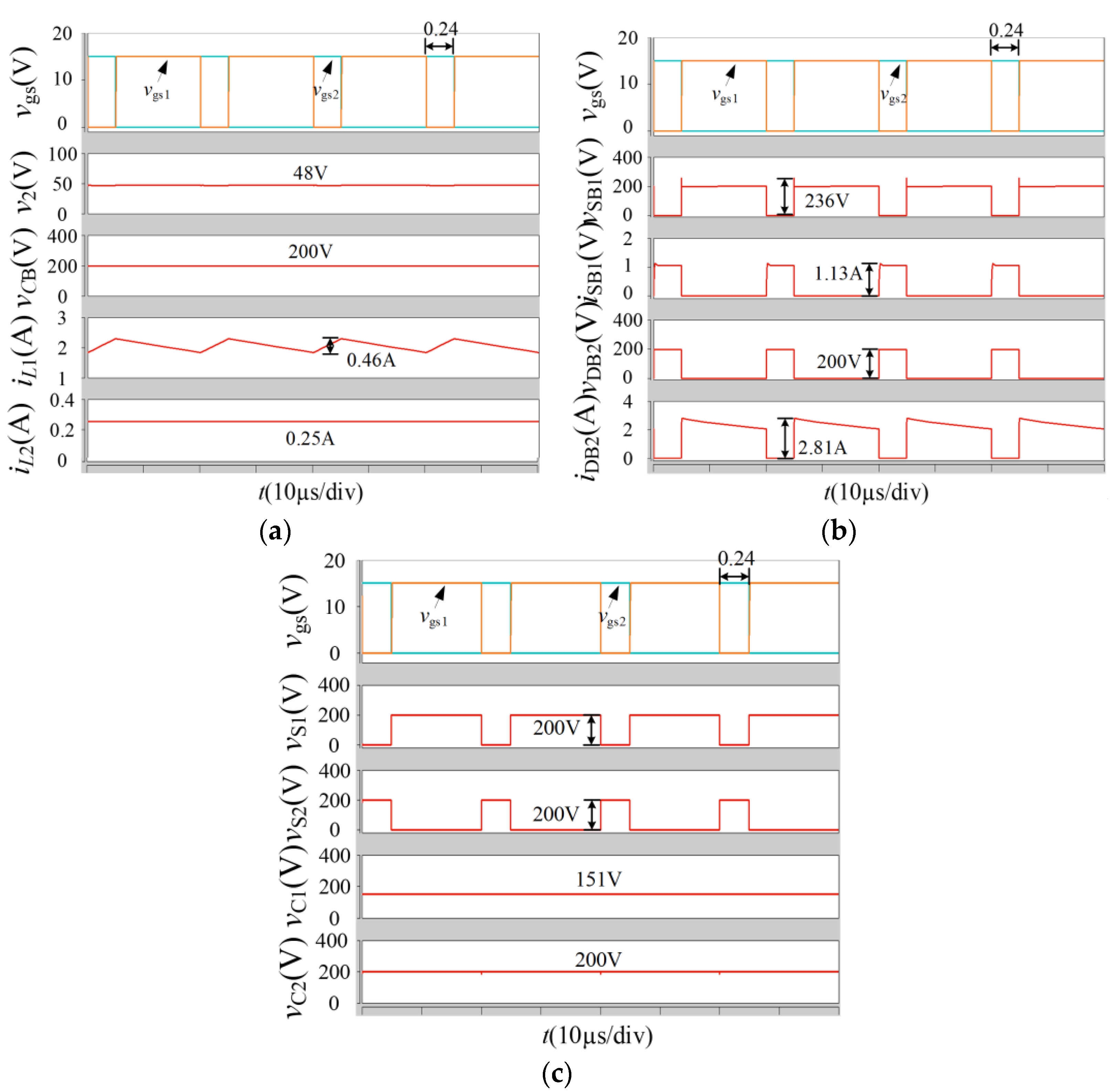
4.1.1. Voltage and Current Waveform of Steady State
4.1.2. Ripple Characteristics
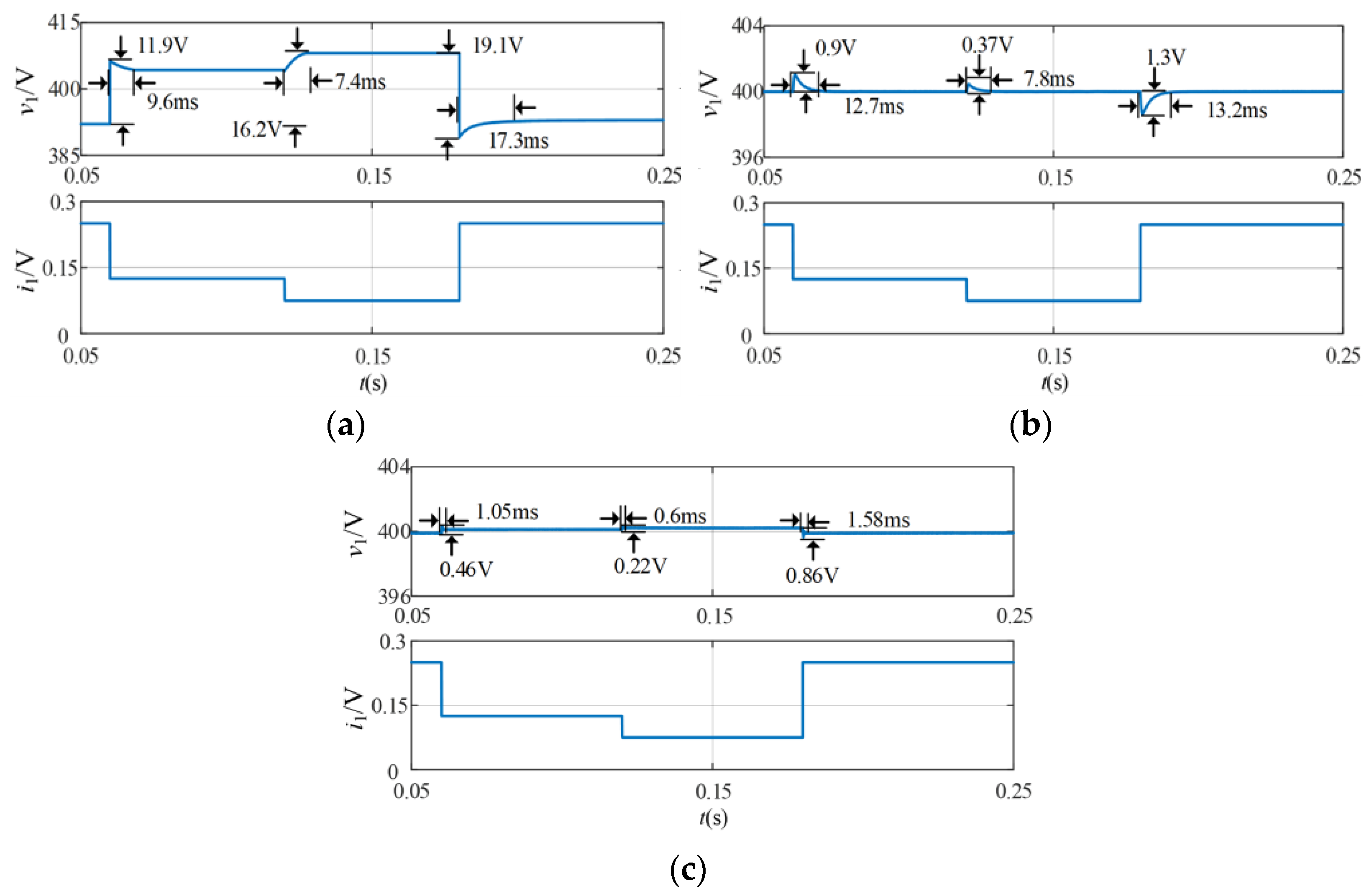
4.1.3. Dynamic Characteristics
4.2. Experimental Results
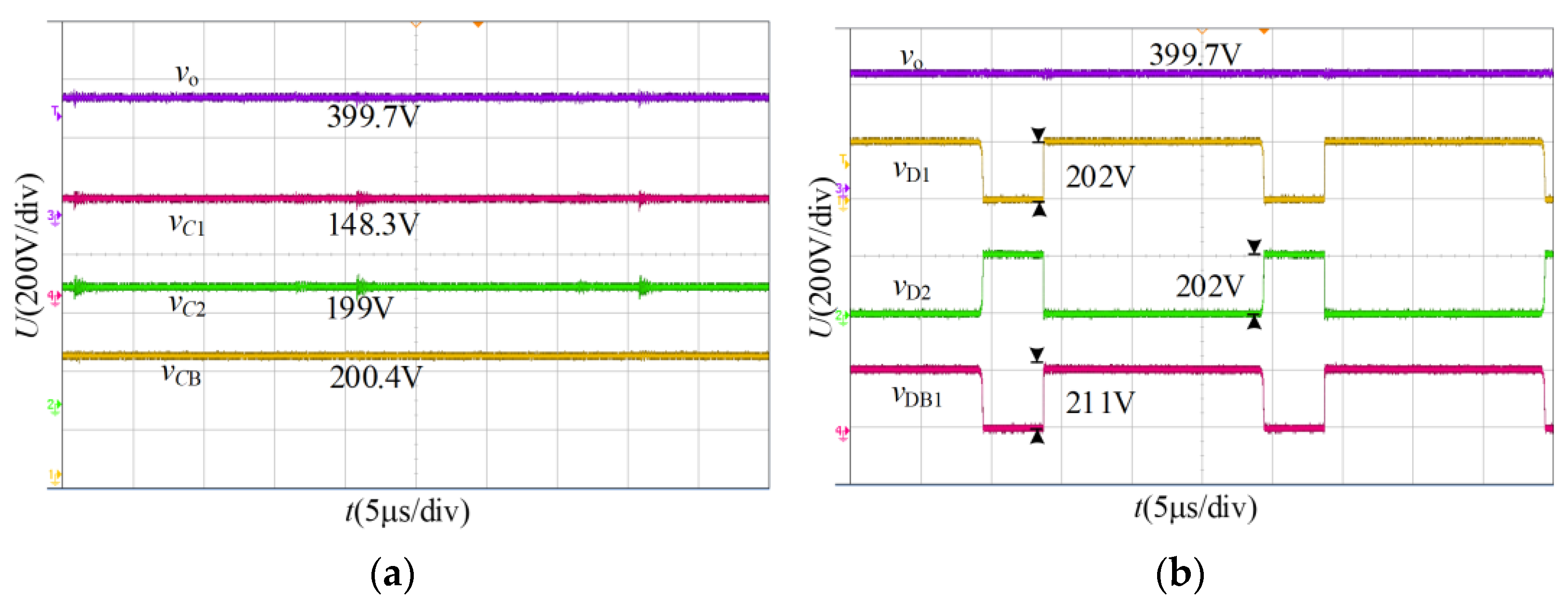
4.2.1. Voltage and Current Waveform of Steady State
4.2.2. Ripple Characteristics
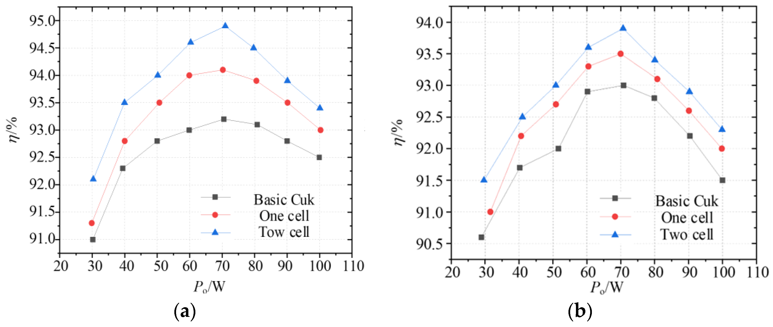
4.2.3. Efficiency Characteristics
4.2.4. Dynamic Characteristics
5. Discussion
6. Conclusions
Author Contributions
Funding
Institutional Review Board Statement
Informed Consent Statement
Data Availability Statement
Conflicts of Interest
References
- Onea, F.; Rusu, E. An Evaluation of Marine Renewable Energy Resources Complementarity in the Portuguese Nearshore. J. Mar. Sci. Eng. 2022, 10, 1901. [Google Scholar] [CrossRef]
- Koričan, M.; Perčić, M.; Vladimir, N.; Alujević, N.; Fan, A. Alternative Power Options for Improvement of the Environmental Friendliness of Fishing Trawlers. J. Mar. Sci. Eng. 2022, 10, 1882. [Google Scholar] [CrossRef]
- Taghavi, S.S.; Rezvanyvardom, M.; Mirzaei, A.; Gorji, S.A. High Step-Up Three-Level Soft Switching DC-DC Converter for Photovoltaic Generation Systems. Energies 2023, 16, 41. [Google Scholar] [CrossRef]
- Liu, F.X.; Pan, Z.Z.; Ruan, X.B. Soft-Switching Analysis of a Boost-integrated Bidirectional Active Bridge DC/DC Converter. Proc. CSEE 2013, 33, 44–51. [Google Scholar]
- Guo, H.W.; Wu, X.Z.; Wang, W. Novel Bidirectional Isolated DC/DC Converter Without Reactive Power Circulation. Proc. CSEE 2018, 38, 201–208. [Google Scholar]
- Chengshan, W.; Zhen, W.; Peng, L. High efficiency power extraction control method for direct-drive linear wave energy converters based on forced resonance. J. Trans. China Electrotech. Soc. 2014, 29, 2624–2630. [Google Scholar]
- Pires, V.F.; Foito, D.; Cordeiro, A. A DC-DC Converter with Quadratic Gain and Bidirectional Capability for Batteries/Supercapacitors. IEEE Trans. Ind. Appl. 2018, 54, 274–285. [Google Scholar] [CrossRef]
- Zhang, H.; Chen, Y.; Shin, C.S.; Park, S.J.; Kim, D.H. Transformerless Bidirectional DC-DC Converter for Battery Storage System with High Voltage Gain. In Proceedings of the International Conference on Power Electronics and ECCE Asia, Busan, Republic of Korea, 27–30 May 2019. [Google Scholar]
- Gunasekaran, D.; Qin, L.; Karki, U.; Li, Y.; Peng, F.Z. A Variable (n/m)X Switched Capacitor DC-DC Converter. IEEE Trans. Power Electron. 2017, 32, 6219–6235. [Google Scholar] [CrossRef]
- Zhang, Y.; Gao, Y.P.; Zhou, L.; Sumner, M. A Switched-Capacitor Bidirectional DC-DC Converter With Wide Voltage Gain Range for Electric Vehicles With Hybrid Energy Sources. IEEE Trans. Power Electron. 2018, 33, 9459–9469. [Google Scholar] [CrossRef]
- Hong, C.M.; Yang, L.S.; Liang, T.J.; Chen, J.F. Novel bidirectional DC-DC converter with high step-up/down voltage gain. In Proceedings of the 2009 Energy Conversion Congress and Exposition, San Jose, CA, USA, 20–24 September 2009. [Google Scholar]
- Akhormeh, A.; Abbaszadeh, K.; Moradzadeh, M.; Shahirinia, A. High Gain Bidirectional Quadratic DC-DC Converter Based on Coupled Inductor with Current Ripple Reduction Capability. IEEE Trans. Ind. Electron. 2021, 68, 7826–7837. [Google Scholar] [CrossRef]
- Zhang, Y.; Liu, Q.Q. Hybrid Switched Capacitor Switched Quasi-Z-Source Bidirectional DC–DC Converter With a Wide Voltage Gain Range for Hybrid Energy Sources EVs. IEEE Trans. Ind. Electron. 2019, 66, 2680–2690. [Google Scholar] [CrossRef]
- Wu, L.T.; Yang, Z.H.; Xu, B.G. Investigation of Passivity-Based Control of DC-DC Converter. Trans. China Electrotech. Soc. 2004, 19, 66–69. [Google Scholar]
- Cui, J.; Wang, J.H. Study of Passivity-Based Control of Buck Converter Based on Optimal Damping Injection. J. Electr. Eng. 2018, 13, 7–13. [Google Scholar]
- Mihaly, V.; Susca, M.; Dobra, P. Passivity-Based Controller for Nonideal DC-to-DC Boost Converter. In Proceedings of the 2019 22nd International Conference on Control Systems and Computer Science (CSCS), Bucharest, Romania, 28–30 May 2019. [Google Scholar]
- Hu, J.W.; Wang, J.H.; Tang, Q. Research on A New Type of High Gain Cuk Converter. Trans. China Electrotech. Soc. 2004, 19, 66–69. [Google Scholar]
- Kim, T.W.; Park, S.K.; Ahn, H.H.; Yoon, S.S. Robust Passivity Based Control with Sliding Mode for DC-to-DC Converters. In Proceedings of the International Joint International on SICE-ICASE IEEE, Busan, Republic of Korea, 18–21 October 2006. [Google Scholar]
- Hassan, M.A.; Li, E.P.; Li, X.; Duan, C.; Chi, S. Adaptive Passivity-Based Control of dc-dc Buck Power Converter With Constant Power Load in DC Microgrid Systems. IEEE J. Emerg. Sel. Top. Power Electron. 2019, 7, 2029–2040. [Google Scholar] [CrossRef]
- Ortega, R.; Garcia-Canseco, E. Interconnection and damping assignment passivity-based control: A. survey. Eur. J. Control 2004, 10, 432–450. [Google Scholar] [CrossRef]
- Gaviria, C.; Fossas, E.; Griñó, R. Robust controller for a full-bridge rectifier using the IDA approach and GSSA modeling. IEEE Trans. Circuits Syst. I Reg. Pap. 2005, 52, 609–616. [Google Scholar] [CrossRef]
- Dòria-Cerezo, A. Modeling, simulation and control of doubly-fed induction machine controlled by back-to-back converter. Ph.D. Dissertation, Department Control Industrial System, Polytechnic University of Catalonia, Barcelona, Spain, 2006. [Google Scholar]
- Cornea, O.; Andreescu, G.D.; Muntean, N.; Hulea, D. Bidirectional Power Flow Control in a DC Microgrid Through a Switched-Capacitor Cell Hybrid DC-DC Converter. IEEE Trans. Ind. Electron. 2017, 64, 3012–3022. [Google Scholar] [CrossRef]
- Romeo, O.; Perez, L. Passivity-based Control of Euler Lagrange Systems. Adapt. Disturb. Attenuation Frict. Compens. 1998, 26, 75–92. [Google Scholar]
- Chen, H.X. Study on a High Gain Bidirectional DC-DC Cuk Converter and Its Nonlinear Control Strategy; Fuzhou University: Fuzhou, China, 2021. [Google Scholar]


| Bidirectional Converter | Max. Voltage Stress of Switches | Efficiency | Structural Complexity | NS | Ripple | Voltage Gain | |
|---|---|---|---|---|---|---|---|
| Step-Up | Step-Down | ||||||
| Buck/Boost Converter | VH | - | simple | 2 | large | D | |
| Converter described in [23] | VH | 88.9~92.3% (250 W) | complex | 4 | large | D2 | |
| Converter in [24] (one-cell) | - | complex | 3 | low | |||
| Proposed Converter | 91.5~94.8% (100 W, two-cell) | complex | 4 | low | |||
| Parameters | Value | Parameters | Value |
|---|---|---|---|
| Po/W | 100 | C1–C2 | 20 uF/630 V |
| V1/V | 400 (300–450) | CB | 20 uF/630 V |
| V2/V | 48 (36–60) | Co1 | 100 uF/450 V |
| L1/mH | 1.2 | Co2 | 100 uF/160 V |
| L2/mH | 1.2 | SB1–SB2 | SVD12N65T |
| fs/kHz | 50 | S1–S2 | FCP099N65S3 |
| PBC | PBC with PI | PBC with LADRC | ||||
|---|---|---|---|---|---|---|
| Input voltage | Overshoot | Recovery time | Overshoot | Input voltage | Overshoot | Recovery time |
| 36–48 V | 6.83V | 120 ms | 4.75 V | 86 ms | 4.37 V | 19 ms |
| 48–36 V | −4.1V | 154 ms | −1.94 V | 80 ms | −1.38 V | 40 ms |
| 36–60 V | 9.5V | 192 ms | 5.7 V | 98 ms | 4.74 V | 46 ms |
| 60–36 V | −5.5V | 213 ms | −2.14 V | 103 ms | −1.79 V | 89 ms |
| PBC | PBC with PI | PBC with LADRC | ||||
|---|---|---|---|---|---|---|
| Input voltage | Overshoot | Recovery time | Overshoot | Input voltage | Overshoot | Recovery time |
| 0.12–0.25 A | −2.31 V | 39 ms | −2.34 V | 87 ms | −1.04 V | 19 ms |
| 0.25–0.12 A | 2.1 V | 53 ms | 2.41 V | 83 ms | 0.73 V | 23 ms |
| 0.08–0.25 A | −3.94 V | 78 ms | −4 V | 98 ms | −1.21 V | 63 ms |
| 0.25–0.08 A | 3.69 V | 84 ms | 3.65 V | 104 ms | 0.94 V | 72 ms |
| PBC | PBC with PI | PBC with LADRC | ||||
|---|---|---|---|---|---|---|
| Input voltage | Overshoot | Recovery time | Overshoot | Recovery time | Overshoot | Recovery time |
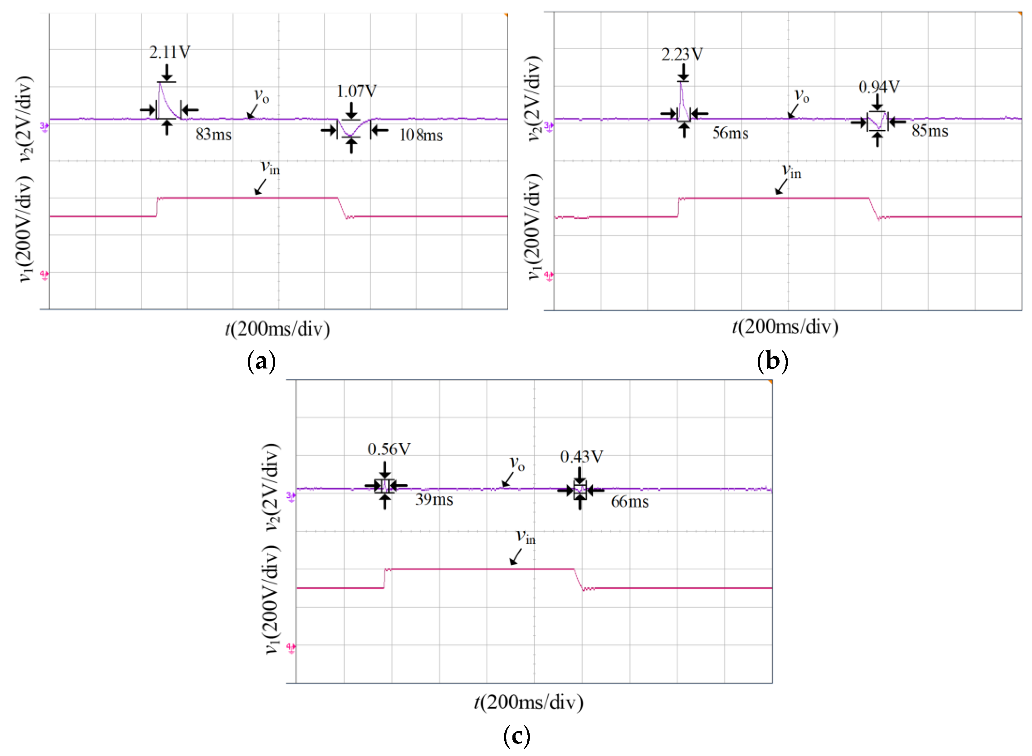
| 300–400 V | 2.11 V | 83 ms | 2.23 V | 56 ms | 0.56 V | 39 ms |
| 400–300 V | −1.07 V | 108 ms | −0.94 V | 85 ms | −0.43 V | 66 ms |
| 400–450 V | 2.11 V | 83 ms | 2.23 V | 56 ms | 0.56 V | 39 ms |
| 450–400 V | −1.07 V | 108 ms | −0.94 V | 85 ms | −0.43 V | 66 ms |
| PBC | PBC with PI | PBC with LADRC | ||||
|---|---|---|---|---|---|---|
| Input voltage | Overshoot | Recovery time | Overshoot | Input voltage | Overshoot | Recovery time |
| 1.04–2.08 A | −0.93 V | 58 ms | −1.05 V | 37 ms | −0.24 V | 26 ms |
| 2.08–1.04 A | 0.72 V | 66 ms | 1 V | 34 ms | 0.31 V | 29 ms |
| 0.63–2.08 A | −2.17 V | 75 ms | −2.08 V | 54 ms | −0.62 V | 38 ms |
| 2.08–0.63 A | 2.32 V | 87 ms | 1.81 V | 53 ms | 0.7 V | 42 ms |
Disclaimer/Publisher’s Note: The statements, opinions and data contained in all publications are solely those of the individual author(s) and contributor(s) and not of MDPI and/or the editor(s). MDPI and/or the editor(s) disclaim responsibility for any injury to people or property resulting from any ideas, methods, instructions or products referred to in the content. |
© 2023 by the authors. Licensee MDPI, Basel, Switzerland. This article is an open access article distributed under the terms and conditions of the Creative Commons Attribution (CC BY) license (https://creativecommons.org/licenses/by/4.0/).
Share and Cite
Chen, H.; Lin, W.; He, W. Research on a DC–DC Converter and Its Advanced Control Strategy Applied to the Integrated Energy System of Marine Breeding Platforms. J. Mar. Sci. Eng. 2023, 11, 512. https://doi.org/10.3390/jmse11030512
Chen H, Lin W, He W. Research on a DC–DC Converter and Its Advanced Control Strategy Applied to the Integrated Energy System of Marine Breeding Platforms. Journal of Marine Science and Engineering. 2023; 11(3):512. https://doi.org/10.3390/jmse11030512
Chicago/Turabian StyleChen, Hongxing, Weiming Lin, and Wei He. 2023. "Research on a DC–DC Converter and Its Advanced Control Strategy Applied to the Integrated Energy System of Marine Breeding Platforms" Journal of Marine Science and Engineering 11, no. 3: 512. https://doi.org/10.3390/jmse11030512
APA StyleChen, H., Lin, W., & He, W. (2023). Research on a DC–DC Converter and Its Advanced Control Strategy Applied to the Integrated Energy System of Marine Breeding Platforms. Journal of Marine Science and Engineering, 11(3), 512. https://doi.org/10.3390/jmse11030512