1. Introduction
The marine DC power supply system in ships is categorized into high-power supplies and low-voltage auxiliary power supplies according to their functions [
1]. Among them, the power supply of all-electric propulsion ships consists of a diesel engine and generator, which is a high-power power supply used to drive the propeller to provide power to the ship. The low-voltage auxiliary power supply is generally composed of battery packs and a DC/DC converter of small- and medium-power power supplies used for the cockpit and the centralized control room for a variety of low-voltage power supplies. In the design requirements of marine DC power supplies, the power quality requirements of the power supply increase as the accuracy and stability requirements of these electronic devices increase. Moreover, due to the very large temperature difference in the maritime environment, the requirements for converter efficiency and temperature rise are relatively high [
2,
3,
4,
5]. In general, compared with the inland power supply, the marine DC power supply has higher requirements for voltage regulation accuracy, conversion efficiency, power density, and other aspects. In order to meet the high-power density requirements of marine DC power supplies, it is feasible and effective to increase the switching frequency. With the extensive use of MOSFETs in power supply equipment, the operating frequency of the converter has been increased, and the requirements for power supplies have been further improved. The LLC resonant converter has received extensive attention and research from scholars all over the world because of its simple topology, ability to realize zero-voltage switching over a wide load range, and thus its high efficiency in power transfer [
6,
7,
8].
When the switching frequency is higher or lower than the resonant frequency point, the LLC resonant converter will reduce or increase its voltage gain, so that the output voltage of the converter can be regulated by the variable frequency control technique. In order to obtain an accurate relationship between the voltage gain and switching frequency, scholars have proposed many modeling methods, such as the first harmonic approximation, extended description function, and generalized mean models [
9,
10,
11]. However, these modeling methods often do not consider circuit parasitic parameters such as the junction capacitors of MOSFET and the diodes. These can lead to an insufficient accuracy when analyzing the problems that exist under different operating conditions. For example, in the marine DC power supply system, the energy storage battery will operate in light load or very light load conditions during the charging process. This will lead to the problem of the voltage gain rising instead of decreasing when the switching frequency of the LLC resonant converter is higher than the resonance frequency, thus affecting the voltage regulation and deteriorating the control performance. Ref. [
12] develops an impedance model that posits this problem is due to the secondary diode junction capacitor and proposes an improved circuit topology to solve it, but it does not consider the effect of switching junction capacitors, so their analysis is not comprehensive enough. This approach is also used in [
13] to analyze the light load performance, but also without considering the parasitic parameters of the switching device. Nowadays, most of LLC resonant converters use MOSFET, whose junction capacitor cannot be easily ignored. In order to solve the problem of the sudden change in voltage gain under light load conditions, [
14,
15,
16] propose various modulation methods, but none of them consider the effect of the parasitic parameters of power devices. In the authors’ previous work, an impedance model considering the switching device’s junction capacitor and diode junction capacitor is established to analyze the causes of the sudden change in voltage, and then an improved circuit topology is proposed to solve the problem of the sudden change in voltage under light load conditions [
17].
On the other hand, the marine DC power supply system operates under heavy load conditions when the ship is at full speed, which requires the converter to be able to stabilize the voltage output and at the same time minimize losses as much as possible. The parameters of the resonant tank of the LLC resonant converter directly affect the voltage gain and loss under heavy load conditions, so it is necessary to analyze and optimize them. The impedance model that takes into account the parasitic parameters of power devices is used in [
18] to qualitatively analyze the effect of the resonant tank’s parameters on the voltage gain. However, it does not give quantitative results and focuses only on the dynamic performance affected by the voltage gain and not on the effect of the parameters’ design on losses. Since it is difficult to optimize the dynamic performance corresponding to the loss and voltage gain at the same time, a compromise is needed. With the development of artificial intelligence optimization technology in recent years, many scholars have combined AI with the parameter optimization of converters. Evolutionary algorithms such as bee swarm optimization, particle swarm optimization (PSO), and the genetic algorithm are often used in power supply optimization design [
19,
20,
21]. They utilize large data populations and multiple iterative updates to find the global optimum. And among them, the particle swarm optimization algorithm is simple, practical, and widely used to find optimal solutions. In [
22], a five-stage PSO-based design method is proposed to satisfy three constrained objectives simultaneously. In [
23], the PSO algorithm is used to obtain the optimal operating point over the entire power range of a dual active bridge converter, which improves the system efficiency. In [
24], the multi-objective optimization design method is also used for inductive power transfer systems to achieve a high-efficiency, high-power-density, and low-stray electric field. However, none of the above studies considered the parasitic parameters of the power devices in their objective function, and only a few of them simultaneously considered both the converter’s dynamic performance and loss as the objective function, which are key indicators of the marine DC power supply system.
Therefore, to improve the performance of the LLC resonant converter in the marine DC power supply system within the full operating range, this paper proposes a full-operating-range optimization design method, which first establishes an impedance model that takes into account the parasitic parameters of power devices on the primary and secondary sides of the transformer. For light load conditions, an auxiliary inductor in series with an auxiliary resistor branch is connected in parallel with the primary side of the transformer in the conventional topology for LLC resonant converter circuits. It solves the problem of the sudden change in voltage gain that occurs when the switching frequency is higher than the resonance frequency under light load conditions. For heavy load conditions, a multi-objective particle swarm parameter optimization algorithm is designed in the method to obtain the optimal resonant tank parameters with the converter loss and voltage gain as the optimization objectives. Then, in order to avoid the loss brought by the auxiliary circuit under heavy load conditions, this paper calculates the critical operating point of the sudden change in the voltage gain and designs a window-switching method to open or close the auxiliary circuit for the appropriate operating condition. Finally, an experimental prototype is designed and constructed, and the effectiveness of the proposed method is verified through experimental results and a comparison with existing research results.
The rest of the paper is organized as follows.
Section 2 introduces and analyzes the performance of the impedance-model-based LLC resonant converter under different operating conditions and draws impedance bode plots to illustrate the aforementioned issues.
Section 3 proposes a full-range operating performance optimization method and gives detailed design steps.
Section 4 verifies the effectiveness of the proposed method by building an experimental prototype and compares it with the existing methods.
Section 5 is the conclusion.
2. Performance Analysis of LLC Resonant Converter Based on Impedance Model under Different Operating Conditions
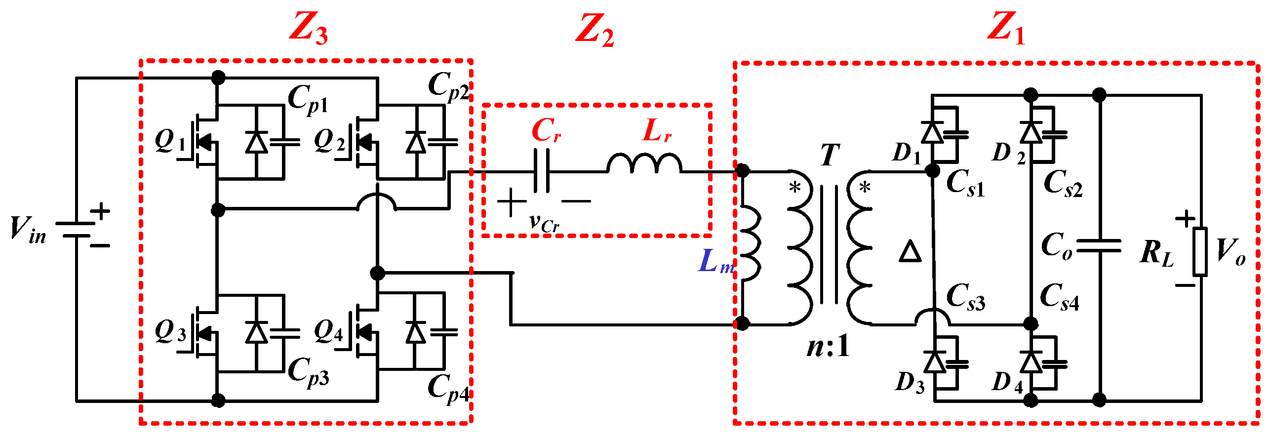
The topology of the LLC resonant converter is shown in
Figure 1, where the resonant inductor, resonant capacitor and magnetic inductor are represented by
Lr,
Cr and
Lm, respectively.
RL and
Co mean the load and output capacitor, respectively. And
T represents the transformer, which turns ratio is
n. The primary side of the transformer adopts a full-bridge structure (
Q1–
Q4), and the secondary side is a rectifier bridge consisting of diodes (
D1–
D4). The design of the parameters in the resonant tank can realize the converter within a wide range of ZVS, and it can also adjust its switching frequency to adjust the voltage gain of the converter so as to achieve voltage regulation. In order to obtain the relationship between the voltage gain and switching frequency, the conventional method mainly uses a fundamental wave analysis to achieve this. However, because it does not take into account the parasitic parameters of the switch and diode, this will lead to a sudden change in the voltage gain when the switching frequency increases to reduce the voltage gain under light load conditions. Meanwhile, when the switching frequency is reduced in order to increase the voltage gain under heavy load conditions, an improper parameter design can lead to the problem that the voltage gain cannot be increased.
To analyze the causes of these problems in depth, this paper considers the parasitic parameters of the power devices and then uses the impedance modeling method to establish the impedance model of the LLC resonant converter, where
Cp and
Cs mean the parasitic capacitor of switching and diode, respectively. This method starts by plotting the topology of the converter circuit into three impedance sections:
Z1,
Z2, and
Z3 as shown in
Figure 1, in which the secondary diode junction capacitor and the load need to be converted to the primary side. By the calculation method proposed by the authors in [
18], the voltage gain
Gc can be calculated as follows.
where
Z1 is the resonant inductance and resonant capacitor and
Z2 is the impedance connected in parallel to the primary side of the transformer. Since the primary-side switching network of the LLC resonant converter is a full-bridge structure, this means that there are always two switching devices with junction capacitor connected in parallel. Therefore, these junction capacitors will change the impedance of the resonant tank, thus adding an impedance cell,
Z3, whose expression is shown below.
where “//” denotes a parallel connection, and
Rac is the equivalent AC resistance of the load
R converted to the transformer’s primary side.
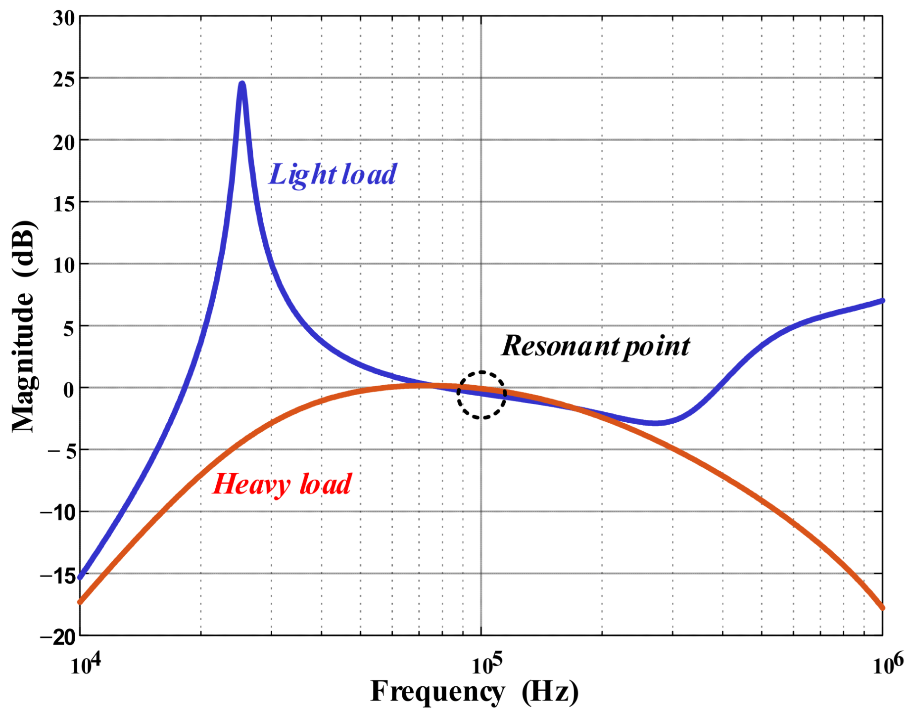
Based on the above voltage gain model, the impedance bode plots can be plotted for light load and heavy load conditions, respectively, as shown in
Figure 2, which gives the relationship between the switching frequency and voltage gain. It can be seen that when the circuit parasitic parameters are taken into account, the voltage gain appears to be abrupt in the high switching frequency under light load conditions and there is insufficient gain in the low switching frequency under heavy load conditions, thus failing to meet the operation and control requirements.
For the voltage gain under heavy load conditions, the authors of this paper proposed a parameter optimization method based on the impedance model in [
18], which improves the voltage gain in the low-frequency band by increasing the value of the resonant capacitor on the basis of the conventional parameter design. For the light load condition, the authors of this paper propose to use the improved LLC resonant converter topology in [
17], which solves the problem of the sudden change in voltage gain in the high-frequency band by connecting an auxiliary inductor in series with an auxiliary resistor branch in parallel on the primary side of the transformer. However, the above method does not consider the whole range of operating conditions, so there are limitations.
3. Full-Operating-Range Performance Optimization Design Method for LLC Resonant Converter
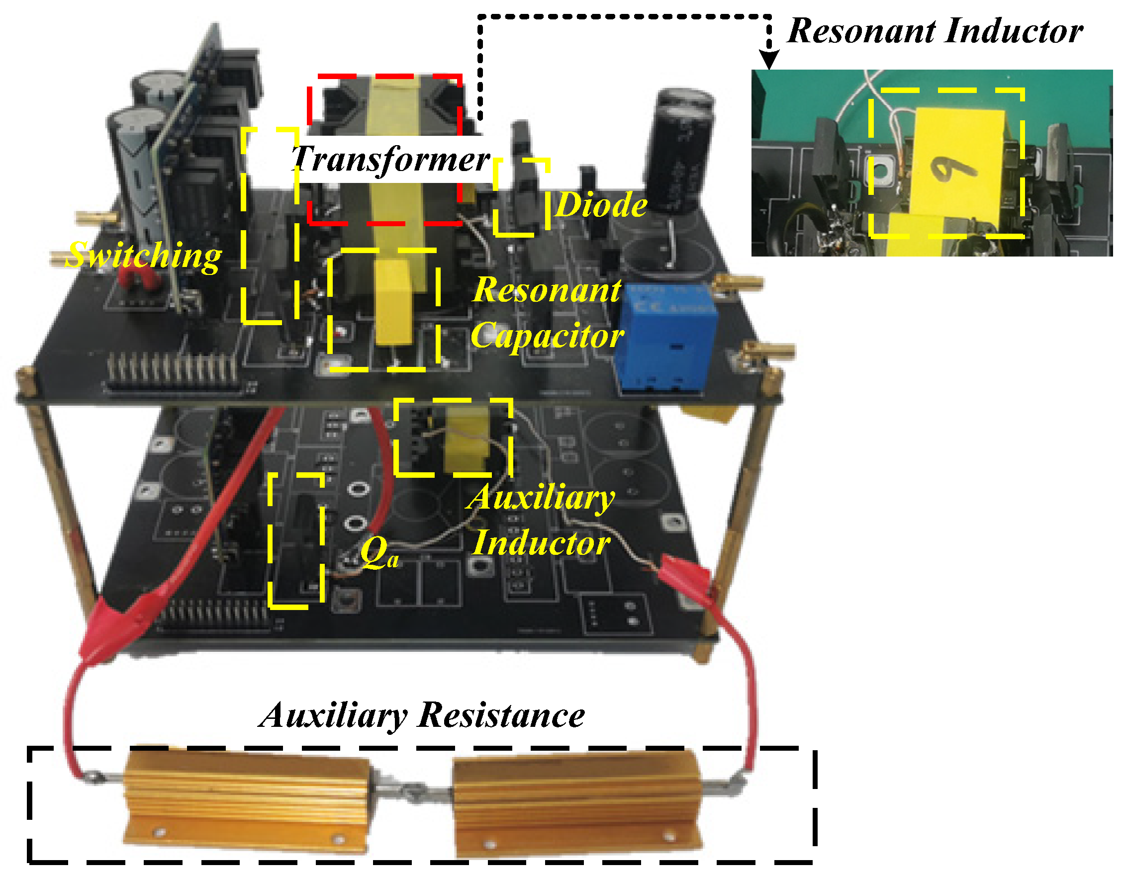
Although the above-proposed methods can solve their corresponding problems under different operating conditions, they have not been effectively combined together. In the marine DC power supply system, the LLC resonant converter not only operates under light load conditions in energy storage, but also under heavy load conditions during its normal operation. Therefore, in order to optimize the performance of the LLC resonant converter within a full range of operating conditions, this paper combines the aforementioned methods for light load and heavy load conditions and deduces their design laws. Then, a full-operating-range performance optimization design method based on the circuit topology of the improved LLC resonant converter is proposed, which adopts the equivalent circuit topology shown in
Figure 3, where
Ladd,
Radd and
Qa mean the auxiliary inductor, auxiliary resistant and auxiliary switching, respectively. Since the LLC resonant converter does not have the problem of the sudden change in voltage gain under heavy load conditions, there is no need to open the auxiliary circuit, and thus a switching device is added to the auxiliary circuit branch to change the auxiliary circuit’s open state under different operating conditions. Therefore, our main focus is on how to optimize the converter parameters under heavy load conditions.
3.1. Multi-Objective Parameter Optimization Method for Heavy Load Conditions
For the performance of the LLC resonant converter system, in addition to its voltage gain, its efficiency is also one of the key design factors, especially under heavy load conditions. Therefore, multiple objectives need to be considered when designing the parameters in order to improve the whole system’s performance. So, the process of solving the multi-objective optimization problem of the LLC resonant converter requires balancing multiple objective functions and seeking a set of compromised optimal solutions. The multi-objective particle swarm algorithm is able to find the optimal solution to the problem by using a population of individuals through an iterative process, so this algorithm is used in this paper to solve the optimal resonant tank parameters of the LLC resonant converter under heavy load conditions. The next step is to first obtain the two objective functions.
3.1.1. Objective Function: Loss Breakdown and Voltage Gain
According to the circuit topology of the LLC resonant converter, its losses are mainly composed of switching losses, transformer losses, and resonant inductor losses.
First of all, in terms of switching losses, there is no turn-on loss because the LLC resonant converter can realize ZVS. Meanwhile, the conduction loss is related to the RMS value of the resonant current, the switch, and diode on-resistance. The turn-off loss is related to the turn-off process switch. Therefore, the switching loss can be expressed as follows.
where the turn-off losses include the primary-side switch’s turn-off losses and secondary-side diode’s turn-off losses.
Secondly, the resonant inductor losses include the core loss and coil loss, which can be obtained by the Steinmetz formula and the copper wire resistance formula, mainly related to the core size, copper wire parameters, switching frequency, the RMS value of the resonant current, etc., which can be expressed as follows.
Finally, the transformer loss and resonant inductor loss calculation methods are basically the same; the difference is that the transformer loss includes the primary side loss and secondary side loss, expressed as follows.
The total loss of the LLC resonant converter, i.e., the loss objective function, can be obtained by summing the above losses.
On the other hand, the voltage gain objective function of the LLC resonant converter can be calculated based on the impedance model in the previous section. From the above two objective functions, it can be seen that they are directly related to the parameters of the resonant tank of the LLC resonant converter, so the optimal parameters can be solved by the multi-objective optimization method.
3.1.2. Multi-Objective Particle Swarm Parameter Optimization Method for LLC Resonant Converter
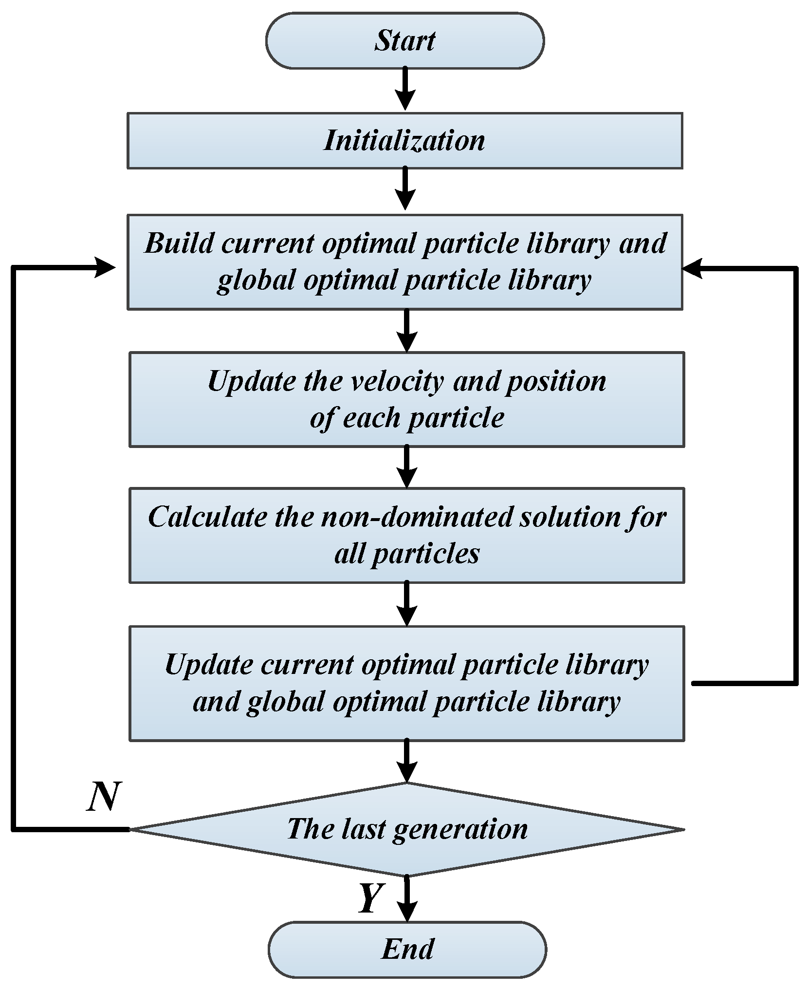
According to the basic principle of the multi-objective particle swarm optimization algorithm, it is known that the parameters will converge to the Pareto optimal frontier after many iterations, so that multiple objectives can reach an optimal combination point.
Figure 4 shows the multi-objective parameter optimization design process.
Firstly, the boundary of the parameters is determined by setting the initial conditions and then taking the ZVS conditions as constraints. Then the weights between the two objective functions are set. Because the converter should first satisfy the dynamic performance and voltage regulation ability, the weight of the voltage gain objective function can be set greater than 0.5. Then the particle information is updated continuously and iteratively by updating the equations of particle velocity and position. The global optimal particle library (GOPL) and current optimal particle library (COPL) are represented by
gopl and
copl, respectively. The specific update equations are shown below.
where
vj and
pj are the velocity and position of the
jth particle;
r() is a stochastic function; and
coplj and
goplj are the current best result of the
jth particle and the global best result of the overall particle, respectively.
k and
n are the current number of iterations and parameter dimensions.
After the number of iterations reaches a preset value, the algorithm stops the calculation and stores the final optimal parameters in GOPL. Since the calculation process will produce a large number of optimal results but not every result meets the practical conditions, further screening is needed. The main purpose of this is to delete the particles with excessive losses and also to consider the ratio of the resonant inductor to the magnetic inductor to prevent effects on the resonance process. In order to ensure the voltage regulation capability under heavy load conditions, the set of resonant cavity element parameters with the highest gain is finally selected.
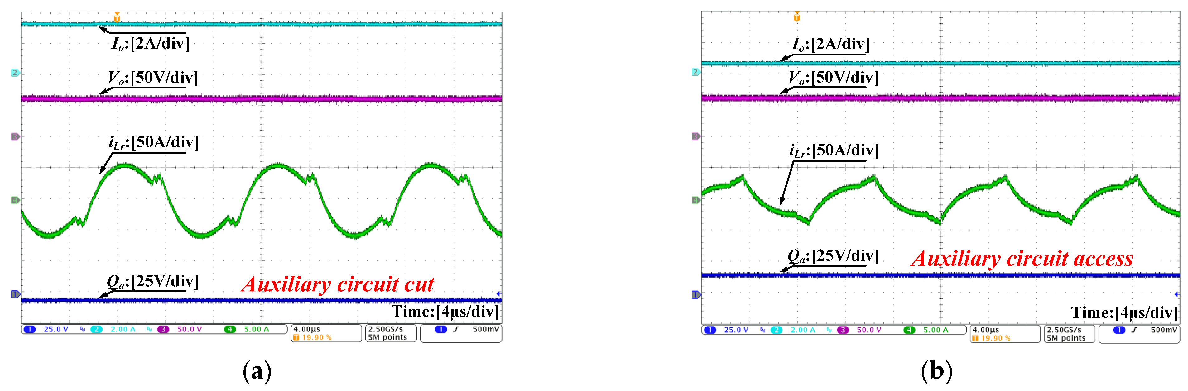
3.2. Critical Operating Point and Window Condition Switching Method
Compared with the circuit topology proposed in [
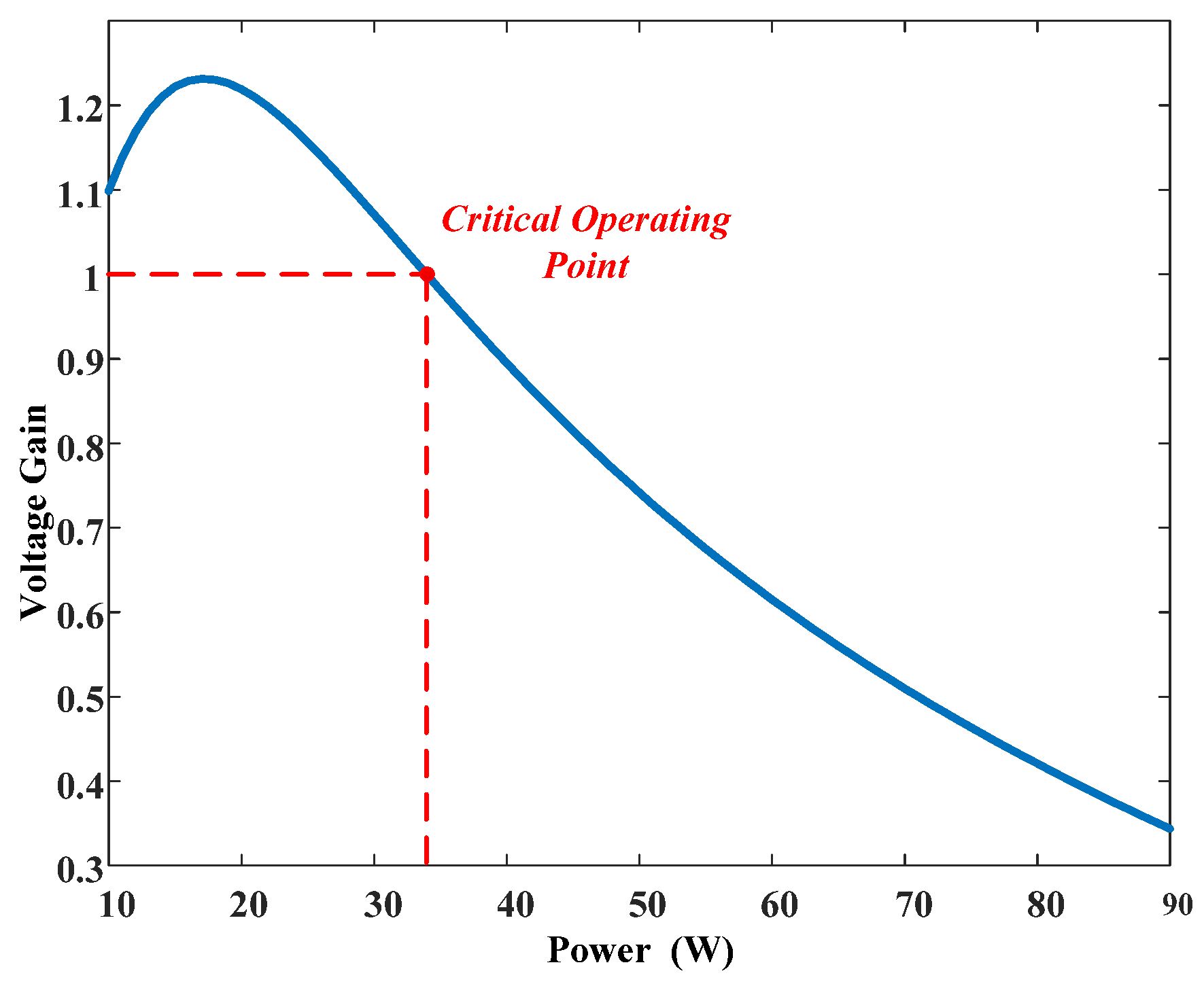
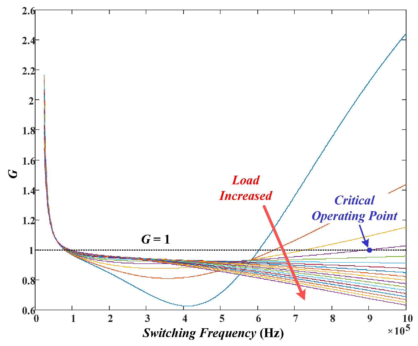
17], a switching device is added to the auxiliary circuit for opening under light load conditions and closing under heavy load conditions. This optimizes the voltage regulation performance under light load conditions and avoids adding excessive losses under heavy load conditions. The role of the auxiliary circuit is to solve the problem of the sudden change in the voltage gain under light load conditions, while such problems do not exist under heavy load conditions. Therefore, in order to determine the appropriate open conditions for the auxiliary circuit, it is necessary to find the critical operating point at which the sudden change in the voltage gain occurs, as shown in
Figure 5.
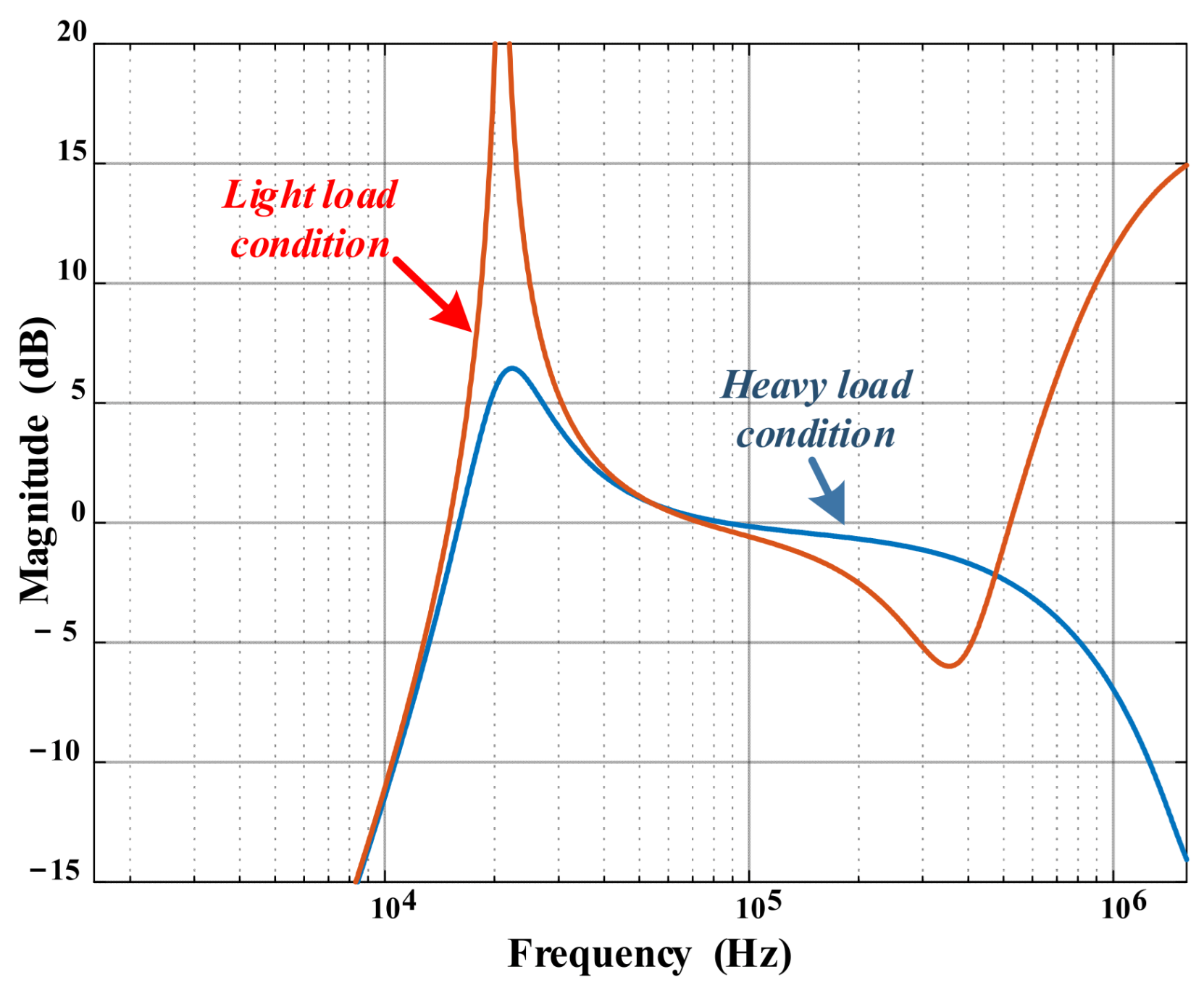
As can be seen from
Figure 5, when the load increases, the degree of the high-frequency band of the sudden change in voltage gain is gradually reduced until the voltage gain is equal to 1. When the load is further increased, the high-frequency band voltage gain is no longer greater than 1, and the phenomenon of the sudden change in voltage gain disappears. Therefore, based on the aforementioned impedance model, this paper calculates the operating conditions in which the voltage gain equals 1 at the high-frequency point, and the specific process is shown below:
First, let
s = 2
πfsj and then convert Equation (1) to the complex frequency domain. Then, the voltage gain
G can be calculated by the amplitude-frequency equation as follows.
The switching frequency point expression for
G = 1 can be calculated from the above equation as follows.
where the expressions for
A,
B,
C, and
D are shown below, respectively.
Then, by deleting the points where the switching frequency is equal to the resonance frequency in the above calculation results, and retaining the expression for the points at which the switching frequency is greater than the resonance frequency, its relationship can be obtained with the load R, i.e., the expression for its relationship with the operating conditions. Because the above expression is more complicated, it is more difficult to solve the critical operating condition point Pc. And there is no need to be too fine when considering the load power, as long as the unit power accuracy can meet the performance requirements. Therefore, the critical operating point can be determined in the mathematical simulation software by substituting a certain power range to plot the gain variation.
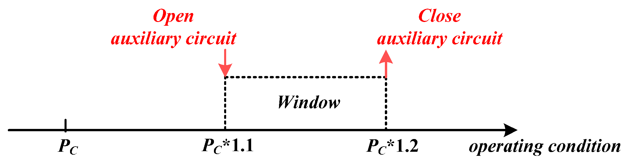
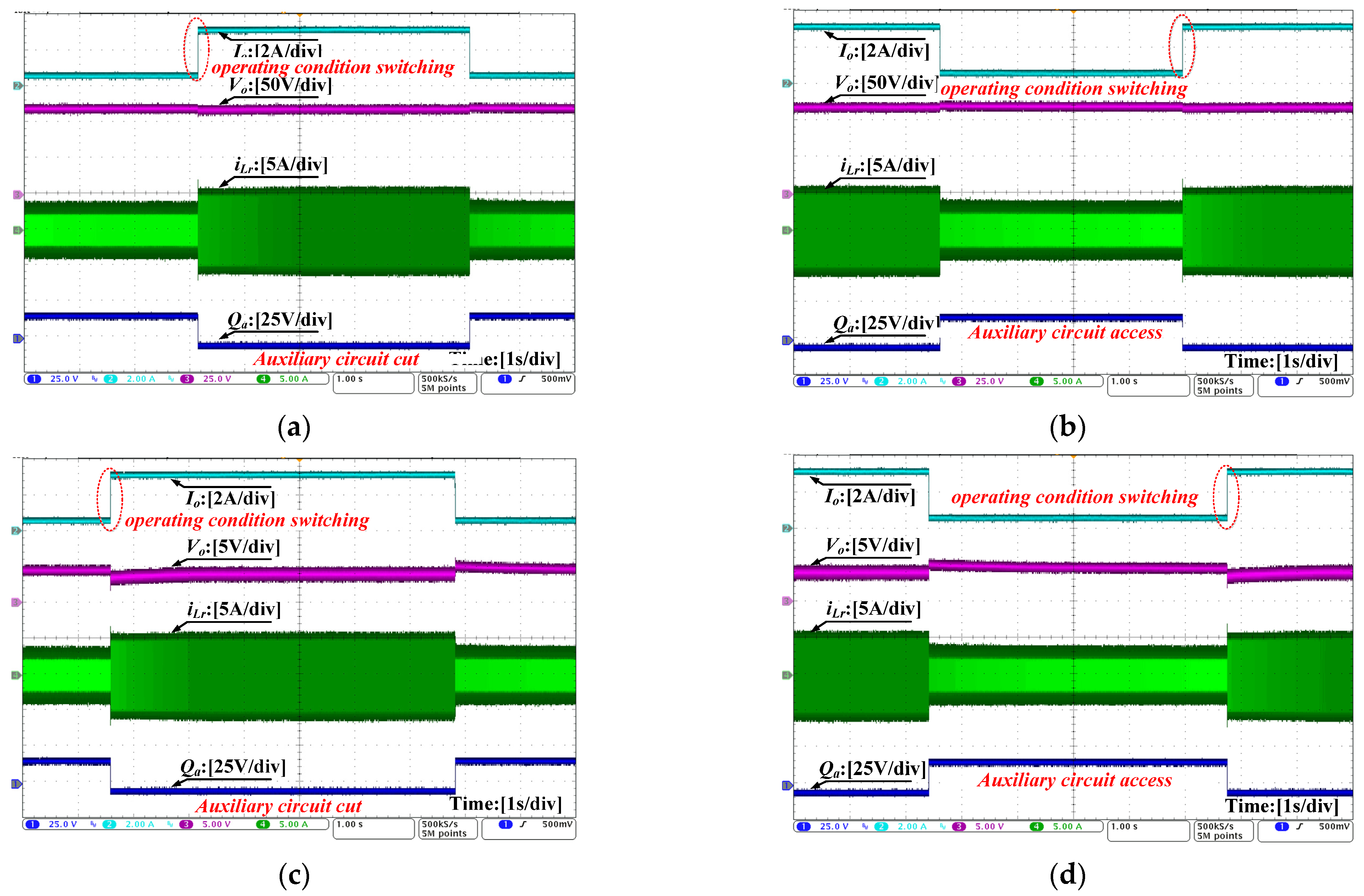
To avoid the frequent opening of auxiliary circuits near the critical operating condition point, this paper adopts the window condition switching method to avoid this problem. First of all, the auxiliary circuit closing conditions are set to more than 20% of the critical operating point. Then, the open conditions of the auxiliary circuit are set to more than 10% of the critical operating point, that is, to avoid the frequent opening and closing the auxiliary circuits brought about by the same operating point and to ensure that the problem of the sudden change in voltage gain before the opening of the auxiliary circuits will not occur. The specific working conditions are shown in
Figure 6.
3.3. Proposed Full-Operating-Range Performance Optimization Design Method
According to the method of auxiliary circuit design by the authors of this paper in a previous research work, it is known that the selection of the auxiliary inductor with the improved circuit topology under light load conditions is consistent with the resonant inductor, while its auxiliary resistance is determined based on the power consumption. Therefore, in order to determine the auxiliary inductor, it is necessary to determine the resonant inductor first. Then, the full-operating-range performance optimization design method for the LLC resonant converter should first start from the multi-objective parameter optimization design for heavy load conditions and finally return to the parameter design for light load conditions, as shown in
Figure 7. The detailed design steps are as follows:
3.3.1. Step 1: Determination of Soft-Switching Conditions
Since the primary side of the converter uses a full-bridge structure with four MOSFETs, the realization of soft switching has a decisive effect on the converter losses and electromagnetic interference, which is mainly realized by charging and discharging the parasitic junction capacitor of the switches by the magnetic inductor current in the dead time. Therefore, the boundary value of the magnetic inductor can be calculated as shown below.
where
n is the turns ratio.
Td and
Czvs are the dead time and junction capacitor, respectively.
3.3.2. Step 2: Loss Calculation
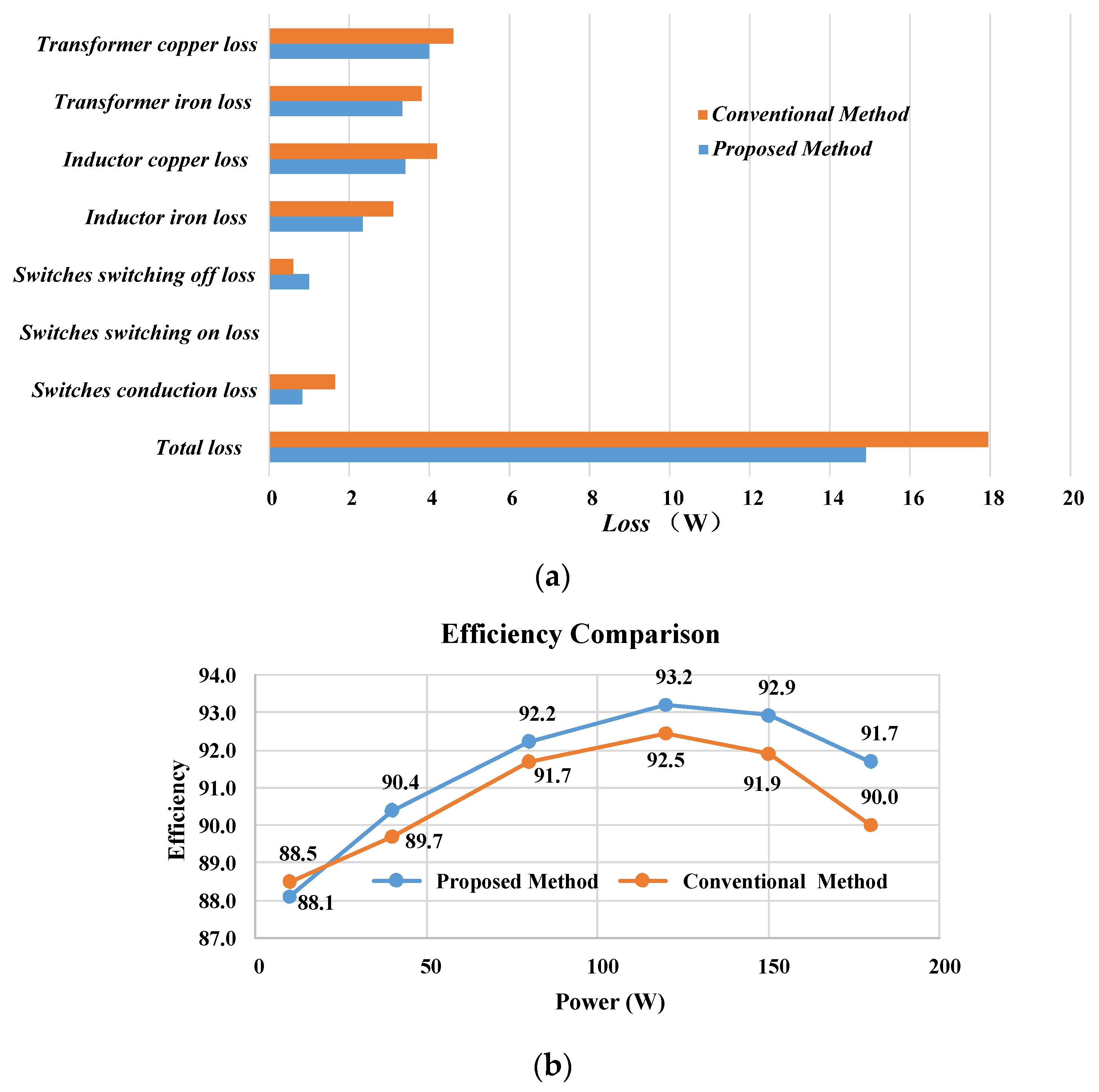
LLC resonant converter loss is one of the core indicators of converter design, which is mainly divided into conduction loss, turn-on loss, turn-off loss, inductor copper loss, inductor iron loss, transformer copper loss, and transformer iron loss. The calculation formulas of these designs are present in a lot of existing research and will not be elaborated in detail here. As different resonant tank parameters can deduce different loss results of the converter, the part of the loss calculation can be used as one of the objective functions of the multi-objective optimization parameter design.
3.3.3. Step 3: Determination of Voltage Gain Calculation
According to the impedance-model-based modeling method, the transformer primary-side impedance
Z2 of the LLC resonant converter with the shunt auxiliary circuit can be recalculated as follows.
where
Ladd and
Radd are the auxiliary inductor and auxiliary resistor, respectively.
Then the above equation can be substituted into Equation (1) to calculate the LLC resonant converter voltage gain at the same frequency. Therefore, in the multi-objective optimization parameter design, the voltage gain calculation can be used as another objective function to determine whether the selected resonant tank parameters can satisfy the voltage gain requirement in the specified frequency band.
3.3.4. Step 4: Multi-Objective Optimized Parameter Design for Heavy Load Condition
The optimal design of the resonant tank parameters using the multi-objective particle swarm parameter optimization method is given in
Section 3.2, with the converter loss and voltage gain as the design objectives, and the specific steps and flowchart are shown in
Figure 4. The resonant tank parameters can be finally determined: the resonant inductor
Lr, the resonant capacitor
Cr, and the magnetic inductance
Lm.
3.3.5. Step 5: Parameter Design for Auxiliary Circuits
According to the method of calculating the parameters of the auxiliary circuit proposed in [
17], the parameters of the auxiliary inductor
Ladd can be determined and selected to be consistent with the resonant inductor
Lr. Then, the auxiliary resistance calculation is shown below, with the auxiliary circuit loss not exceeding 1.5% of the light load power as the upper boundary.
In addition, the selection of the switching device Qa in the auxiliary circuit is mainly based on the transformer primary voltage and the current flowing through the auxiliary circuit. Therefore, considering the voltage withstand margin, the Vds voltage withstand value of Qa should be selected as 1.5 × nVo, and the current withstand value can be calculated according to the calculation process of Radd. According to engineering experience, the margin of 1.5 times these values is considered.
3.3.6. Step 6: Auxiliary Circuit Critical Operating Point Calculation
After the parameters of the auxiliary circuit are determined, the critical operating point for the sudden change in the voltage gain is calculated according to Equation (7), and then the two switching operating condition points of the auxiliary switch are set according to the proposed window-switching method.
Through the above six steps, the resonant tank parameters can be designed to optimize the full-operating-range performance of the LLC resonant converter, and the auxiliary circuit parameters can be designed to solve the problem of the sudden change in voltage gain under light load conditions and improve the output voltage regulation capability under heavy load conditions by using the critical operating condition point of the sudden change in voltage gain.
5. Conclusions
In the power conversion of marine DC power supply systems, the LLC resonant converter is often used, so its performance is very important. However, the parasitic parameters of power devices have a great influence on the system, which leads to different problems under different operating conditions. Under light load conditions, there is a problem of the sudden change in voltage gain when the switching frequency is higher than the resonance frequency. Under heavy load conditions, there is a problem of insufficient voltage gain which affects its voltage regulation. Therefore, this paper combines the authors’ previous research work to propose a full-operating-range performance optimization design method for the LLC resonant converter. It analyzes the causes of the above problems by establishing an impedance model of the converter that takes into account the parasitic parameters of the switch and diode. Then, the problem of the sudden change in the voltage gain in high-frequency band is solved by introducing auxiliary circuits under the light load condition. And under the heavy load condition, the optimal circuit parameters are solved by using the multi-objective particle swarm parameter optimization method with the converter loss and voltage regulation capability as our focuses and the ZVS condition as the constraint. Then the critical condition point and window-switching method are calculated, so that the auxiliary circuit only works in the light load condition to avoid losses in the heavy load condition. Finally, the specific design steps are given, the parameters are designed according to practical operating conditions, and an experimental prototype is built. The effectiveness of the proposed method in this paper is verified by the experimental results, and then the losses are compared with those of the existing solutions and conventional methods to highlight the superiority of the proposed method.


