Article

Low-Cost Rapid Fabrication of Conformal Liquid-Metal Patterns

1
Department of Electrical Engineering, University of Hawaiʻi at Mānoa, Honolulu, HI 96822, USA
2
Center of Excellence, Arab Academy for Science, Technology and Maritime Transport, Smart Village P.O. Box 12577, Egypt
3
Bionano Technology, Gachon University, Seongnam, Gyeonggi 13120, Korea
*
Authors to whom correspondence should be addressed.
Appl. Sci. 2019, 9(8), 1565; https://doi.org/10.3390/app9081565
Submission received: 28 February 2019 / Revised: 8 April 2019 / Accepted: 9 April 2019 / Published: 15 April 2019
(This article belongs to the Special Issue Applications of Liquid Metals)

Abstract

:

Featured Application

Sprayed liquid-metal devices can potentially be used to implement flexible sensors and RF devices.

Abstract

Patterned conformal conductive structures are used to realize flexible electronics for applications such as electronic skin, communication devices, and sensors. Thus, there is a demand for low-cost rapid fabrication techniques for flexible and stretchable conductors. Spray-coating of liquid metals is a prototyping method that is compatible with elastic substrates. In this work, UV-curable and polyimide masks were used to pattern sprayed liquid metal (LM). The effect of the spraying parameters on the thickness and conductivity of the LM was characterized. A minimum LM linewidth of 48 µm was achieved, along with a minimum gap width of 34 µm. A LM patch antenna and transmission line, which can potentially be used for communication systems, were demonstrated using this fabrication process.

Graphical Abstract

1. Introduction

Patterning conformal structures on flexible and stretchable substrates have many applications, such as flexible and stretchable sensors, antennas, or electronic skin. Accordingly, the implementation techniques of such devices should be done with flexible and stretchable materials [1,2,3,4,5] that are optimally compatible with low-cost rapid prototyping. Many low-cost rapid prototyping fabrication techniques have been developed to realize flexible RF devices. Spraying conductive inks have been used in flexible sensors and RF devices for various applications, such as a stretchable RF antenna [6], radio-frequency identification (RFID) antenna [7], optical antenna [8], strain sensors [8], sensors on skin [9,10], and wearable electronics [11]. However, nanoparticle-based conductive inks can form cracks after the solvent evaporates [12,13]. Recently, liquid metals (LM) have been used as an alternative to nanoparticle conductive inks to realize flexible electronics. Like conductive inks, a LM such as Galinstan (a eutectic alloy of gallium, indium, and tin) can be sprayed to create conductive features on flexible substrates. Using a shadow mask to pattern sprayed Galinstan [14] resulted in a minimum line width of 500 µm, but the micromachined mask increased the cost of the fabrication process. A vinyl mask for rapid prototyping was limited to line structures with a minimum width of 200 µm [15]. More complex LM structures were patterned using a screen mesh [16], but the resolution of patterned structures was limited to 234 µm with minimum gaps of 75 µm.
In this paper, we used two types of masks to pattern LM: a UV-curable mask and a polyimide mask. A desktop digital craft cutter was used to cut an adhesive polyimide mask for patterning sprayed LM. Cutting the mask out of polyimide tape is a low-cost method that is compatible with rapid prototyping of complex structures. The polyimide masks were used in conjunction with the spraying of LM to achieve a minimum feature width of less than 50 µm and a minimum gap between LM features of approximately 200 µm. Furthermore, physical scraping of the LM can reduce the gap resolution down to 34 µm. Finally, to prove the viability of using sprayed LM for elements in wireless communication systems, we demonstrated a sprayed LM patch antenna and transmission line. The measured performance of the LM devices was compared to reference copper versions. The sprayed liquid metal process can be used to make stretchable or conformal electronic circuits.

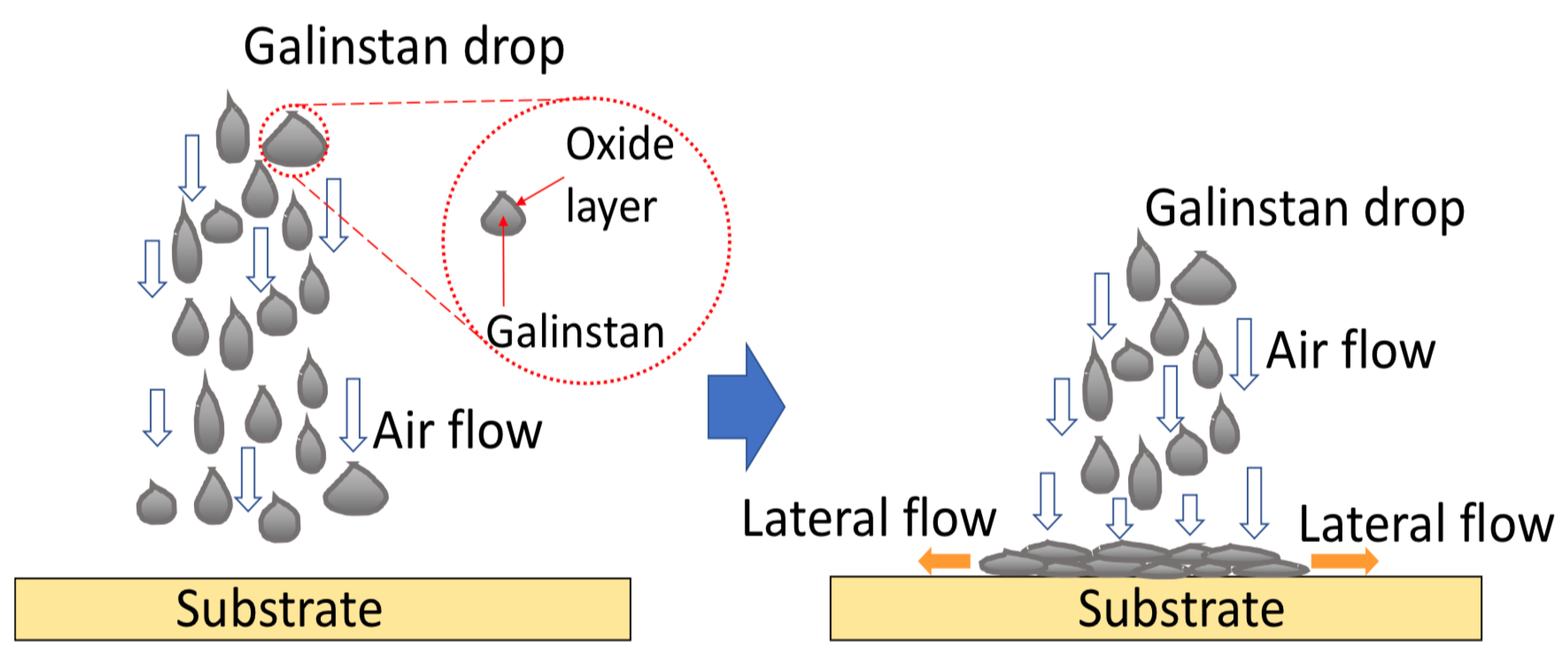
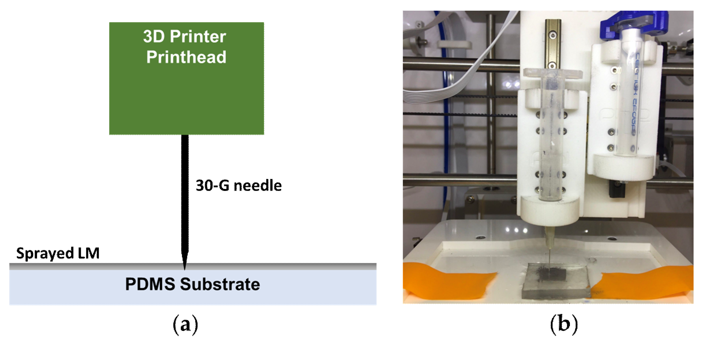
2. Spraying of Galinstan Liquid Metal

Galinstan, which is 68.5% Ga, 21.5% In, and 10% Sn, is a liquid at room temperature, with a conductivity of 3.5 × 10⁶ S/m [17]. A pressurized air gun was used to spray LM, as shown in Figure 1. Once Galinstan is exposed to air it forms a thin oxide film that can coat each LM droplet before it impacts the substrate. The sprayed LM droplets coalesce after hitting the substrate, forming a conductive Galinstan layer covered with the oxide film. Three spraying parameters have been varied in this work: spraying time, spraying distance, and pump pressure.
Flexible UV-curable polyurethane acrylate (PUA) was used to pattern the sprayed LM. Another type of mask made of polyimide tape was cut into patterns using a craft cutter, in a process based on a previous study [18]. The patterned polyimide tape was used as a mask for patterning LM electrodes with different line widths by adhering the tape to the target substrate. The smallest pattern was a single line cut with the craft cutter, which corresponded to an 84-μm-wide cut in the polyimide. The LM was sprayed on Rogers Duroid 5880, glass, and polydimethylsiloxane (PDMS) substrates. An air gun with a nozzle diameter of 300 μm (BBA-003, Beetle Bug) connected to an air compressor was used to spray the LM films. The conductivity of the LM films was obtained by a parameter analyzer (Keithley 4200A-SCS) and a four-point probe. The thickness of the LM sample was measured by a scanning electron microscope (SEM) (JEOL, JSM-7500F). A 1-mm-wide LM line was sprayed on a glass substrate. The thickness of the LM film was measured from the cross-sectional SEM image of the LM film.

3. Results

3.1. Characteristics of Sprayed Galinstan Films

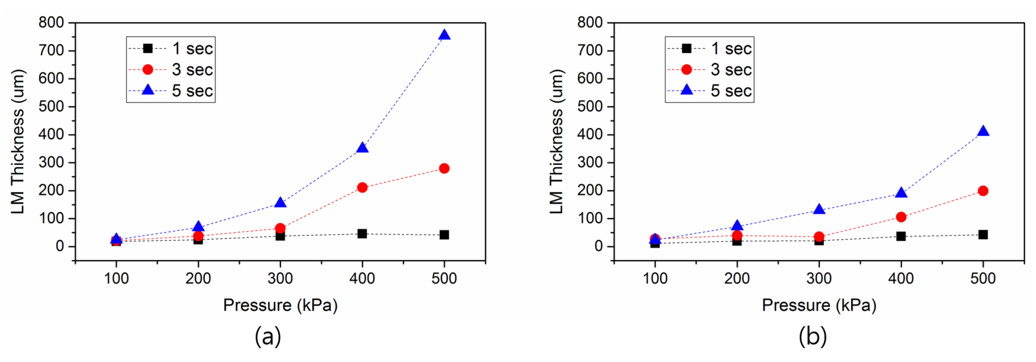
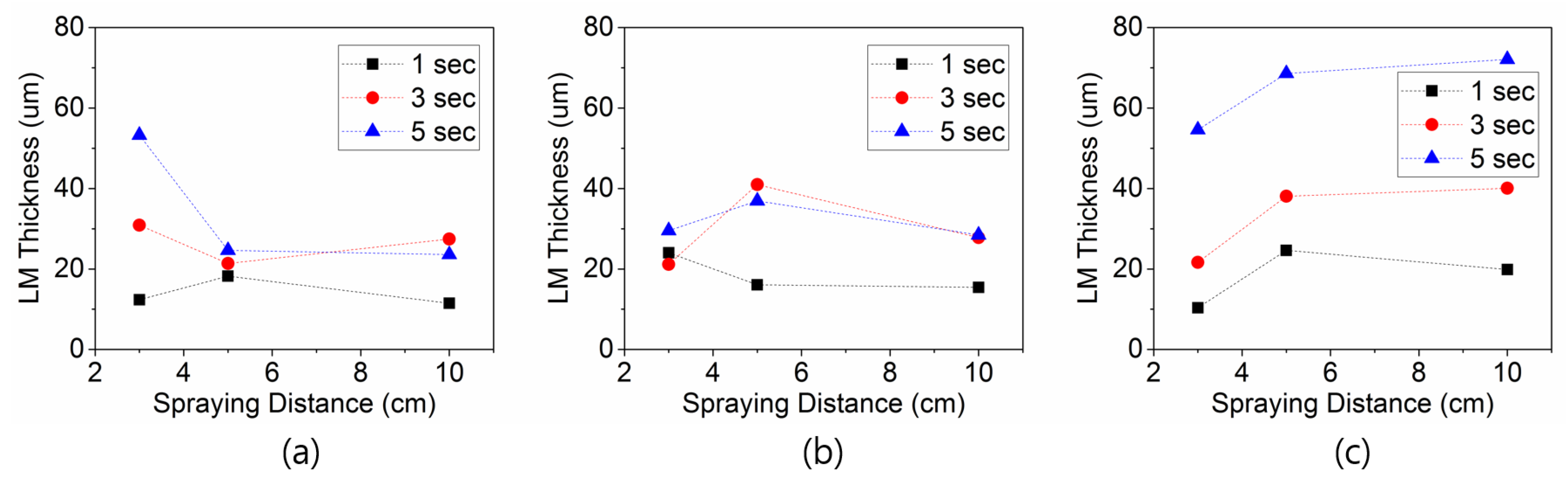
3.1.1. Thickness of LM Films

The thickness of the sprayed LM can be controlled by varying the spraying time and the spraying pressure. The spraying time was varied from 1 s to 5 s, and the spraying pressure was varied from 100 kPa to 500 kPa. The nozzle of the air gun was 5 cm or 10 cm from the target substrate (Figure 2).
As expected, the thickness of the LM film increases as the spraying time increases. The thickness of the LM film decreases as the distance between the nozzle and the substrate increases. The droplets of the sprayed LM disperse as they exit the nozzle of the sprayer, so the sprayed LM covers a larger area when it is sprayed from a greater distance to the substrate. The volume of the sprayed LM was kept constant, so it is expected that the thickness of LM film decreases as the distance increases.
Interestingly, the thickness of the LM films have irregular results when the distance between the nozzle and the substrate is only 3 cm (Figure 3). It is hypothesized that this is due to the effects of the air flow on the LM. During LM deposition, LM droplets and high-pressure air strike the substrate at the same time. Unlike sprayed conductive inks, LM does not contain solvents. Although the LM is covered with a very thin oxide layer, the oxide is fragile enough to break when it is struck by other LM droplets or high-pressure air flow. If the nozzle is close to the substrate, the air can cause lateral flow of LM away from the nozzle, decreasing the LM film thickness.

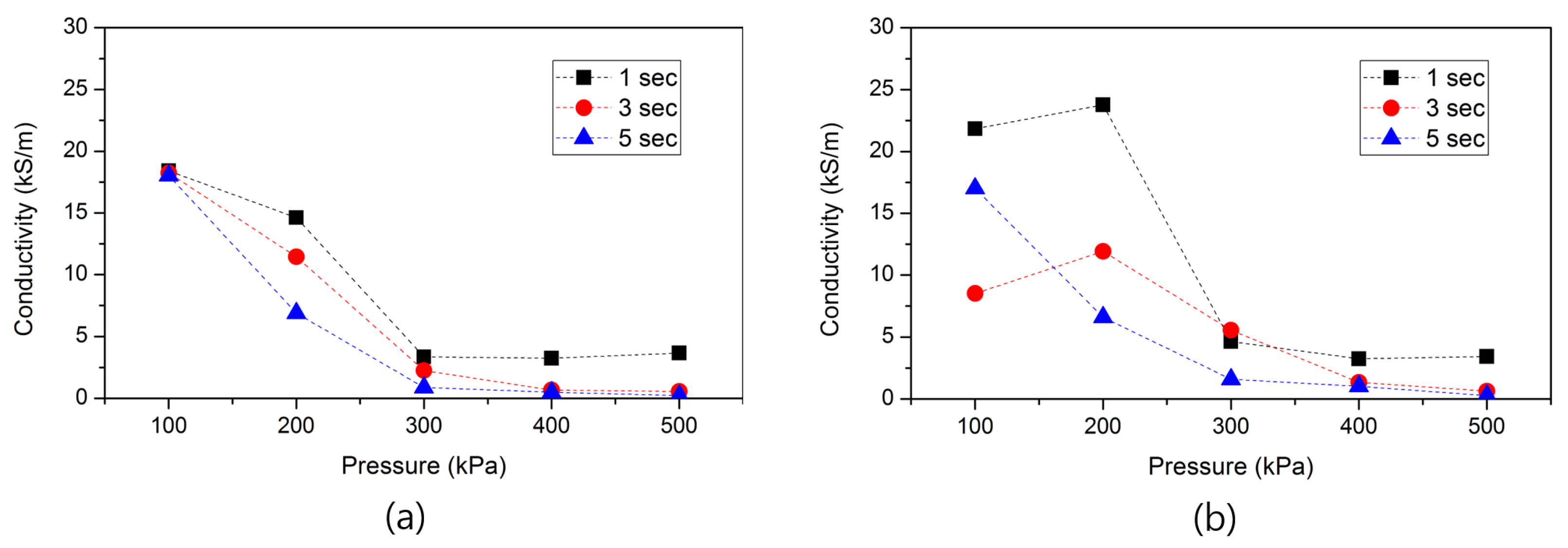
3.1.2. Conductivity of LM Films

To estimate the amount of gallium oxide in the sprayed LM films, the average diameters of LM droplets were measured using a laser scanning microscope. The average droplet diameters were 2.435 μm at 100 kPa, 1.507 μm at 300 kPa, and 0.715 μm at 500 kPa, and the standard deviation of the diameters were 0.2546 μm, 0.1773 μm, and 0.1295 μm, respectively. The thickness of the native gallium oxide of Galinstan was estimated to be approximately 1 to 3 nm [19]. Assuming that the thickness is about 3 nm, the volume fractions of the oxide layer in the LM films sprayed at 100 kPa, 300 kPa, and 500 kPa were 0.37%, 060%, and 1.25%, respectively. Thus, LM films sprayed under higher pressures contain a larger fraction of oxidized LM versus films sprayed at lower pressures, resulting in lower electrical conductivity.
As shown in Figure 4, the conductivity decreases as the thickness of LM film increases. The conductivity per unit thickness of the films should be the same for all sprayed film. However, it decreased due to the increase of oxide formation inside the film. The pressurized air is strong enough to break the outer oxide shell of the LM already deposited on the surface, so the LM that is now exposed to air is rapidly oxidized. Thus, the amount of oxide in the film increases, decreasing the conductivity of thicker LM films with longer spraying times.
LM was sprayed on a nitrile surface to quantify the effect of deformability on the resistance of stretched LM films. As the strain was increased, the resistance of the liquid-metal film also increased (Figure 5) due to the decrease in the thickness of the liquid metal. The resistance steadily increased up to a strain of 80%. When the sample was stretched beyond 80%, the resistance abruptly increased by three orders of magnitude. The same dramatic change in resistance was reported for a metal film under a strain of only 10% [20], and for Ag–Au nanowire electrodes on a PDMS substrate under a strain of 30% [21].

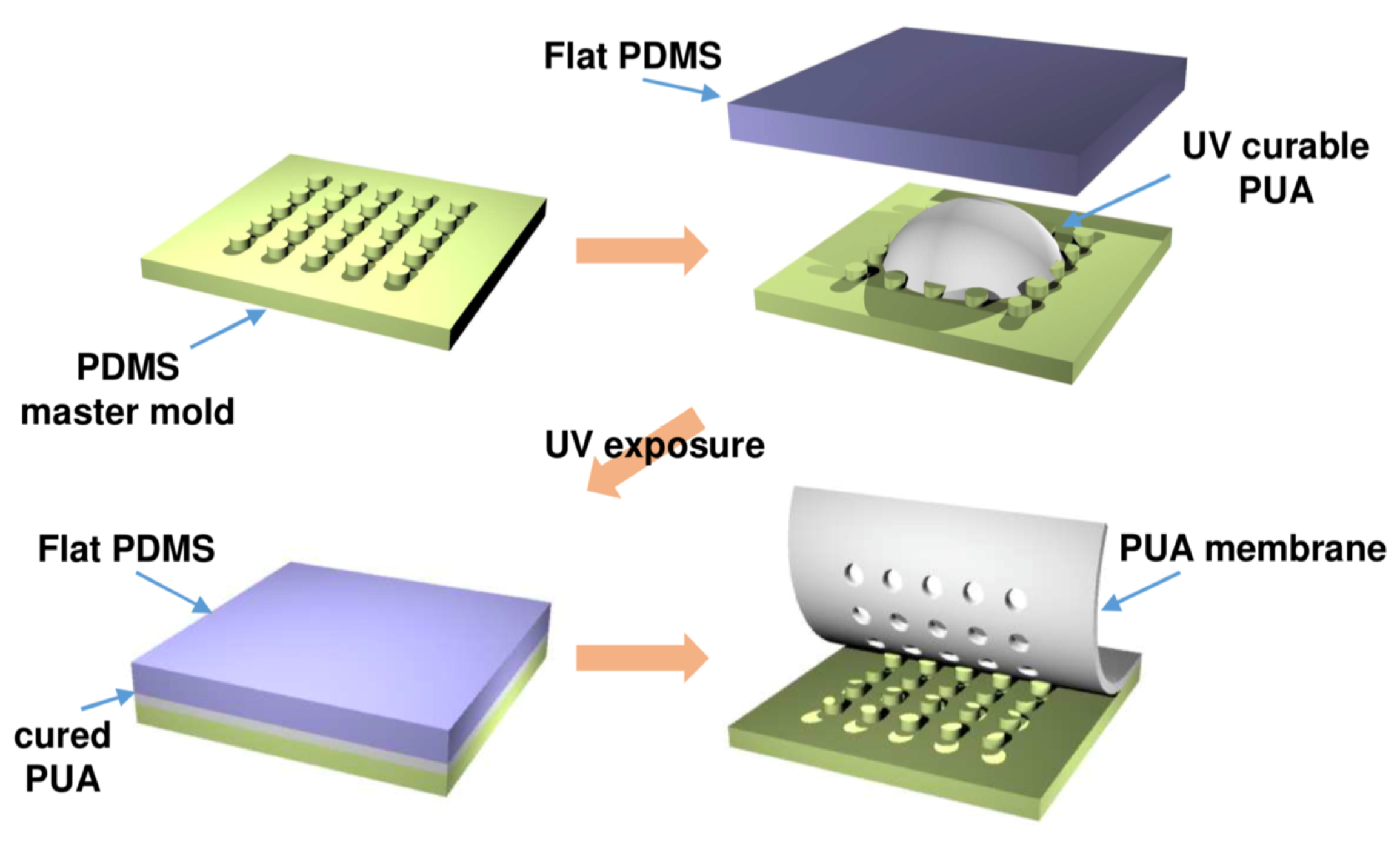
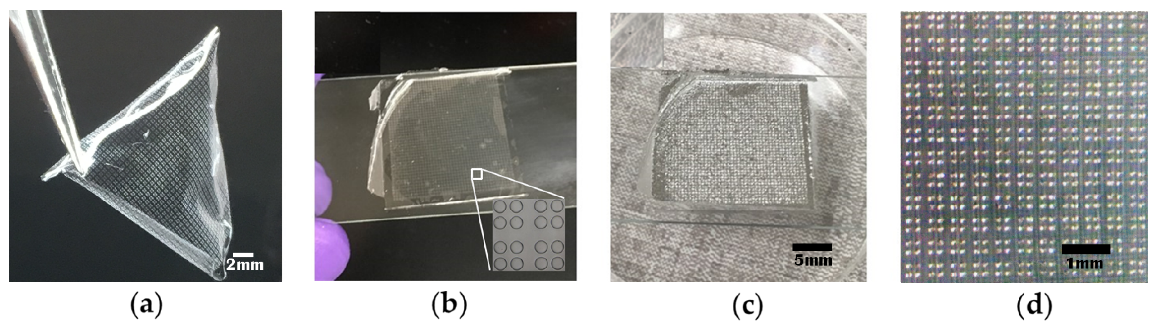
3.2. LM Patterning with a UV-Curable Polymeric Membrane

The sprayed LM thin film can be patterned with UV-curable polymeric masks. The polymeric mask was fabricated by replication from PDMS molds, as introduced in a previous report [22]. The process is shown in Figure 6. A PDMS master mold was prepared, and UV-curable PUA polymer was dropped on the mold. A flat PDMS piece was placed over the PUA and pressed into contact with the lower PDMS mold. The UV-curable PUA polymer was then exposed under a UV lamp for 3 min. Finally, the patterned PUA membrane can be peeled from the mold.
This UV-curable polymeric mask enables us to fabricate minute perforated patterns on the film. In this work, a 2 cm × 2 cm PUA membrane with 150-µm-diameter holes was fabricated (Figure 7a). The PUA mask is slightly sticky, allowing it to conformally contact a smooth glass or plastic substrate. In Figure 7b, the PUA polymeric stencil is placed on a glass microscope slide and the inset is the magnified image of the holes. LM was then uniformly sprayed on the substrate (Figure 7c), and the stencil was carefully peeled off, leaving LM droplets on the glass substrate (Figure 7d). The magnified image of Figure 7d is shown in Figure 8a. LM has a high surface tension, which can make it difficult to separate the shadow mask from the substrate. Thus, there is a limit on the resolution of the LM (~100 μm) when it is patterned using the shadow mask method. Improving the contact of the LM to the substrates could help increase the resolution.
The sprayed LM patterns are shown in Figure 8. In Figure 8a, LM dots with a diameter of 150 µm were transferred to the glass substrate. Each LM pattern has a hemispherical feature because of the high surface tension of Galinstan. Using the PUA mask, it is difficult to fabricate LM patterns smaller than 150 μm. The oxidized surface of the LM makes it difficult to separate it from the polymeric membrane. If the thickness of the LM film is smaller than the feature size, LM can be left on the glass substrate. However, when the size of the pattern is too small, the polymeric membrane can lift all the LM from the surface as the oxidized LM surface sticks to the mask. However, it is easy to create larger patterns, such as a 2-mm letter “C” (Figure 8b) and a simple electrode pattern (Figure 8c). The LM in the letter “C” is 400 µm wide, and the width of the electrode in Figure 8c is 500 µm.

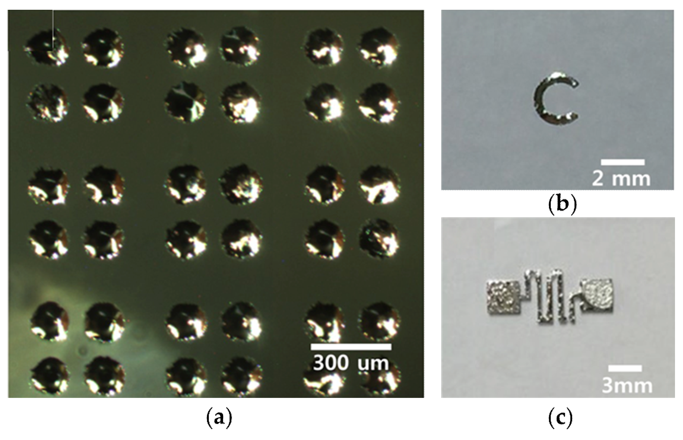
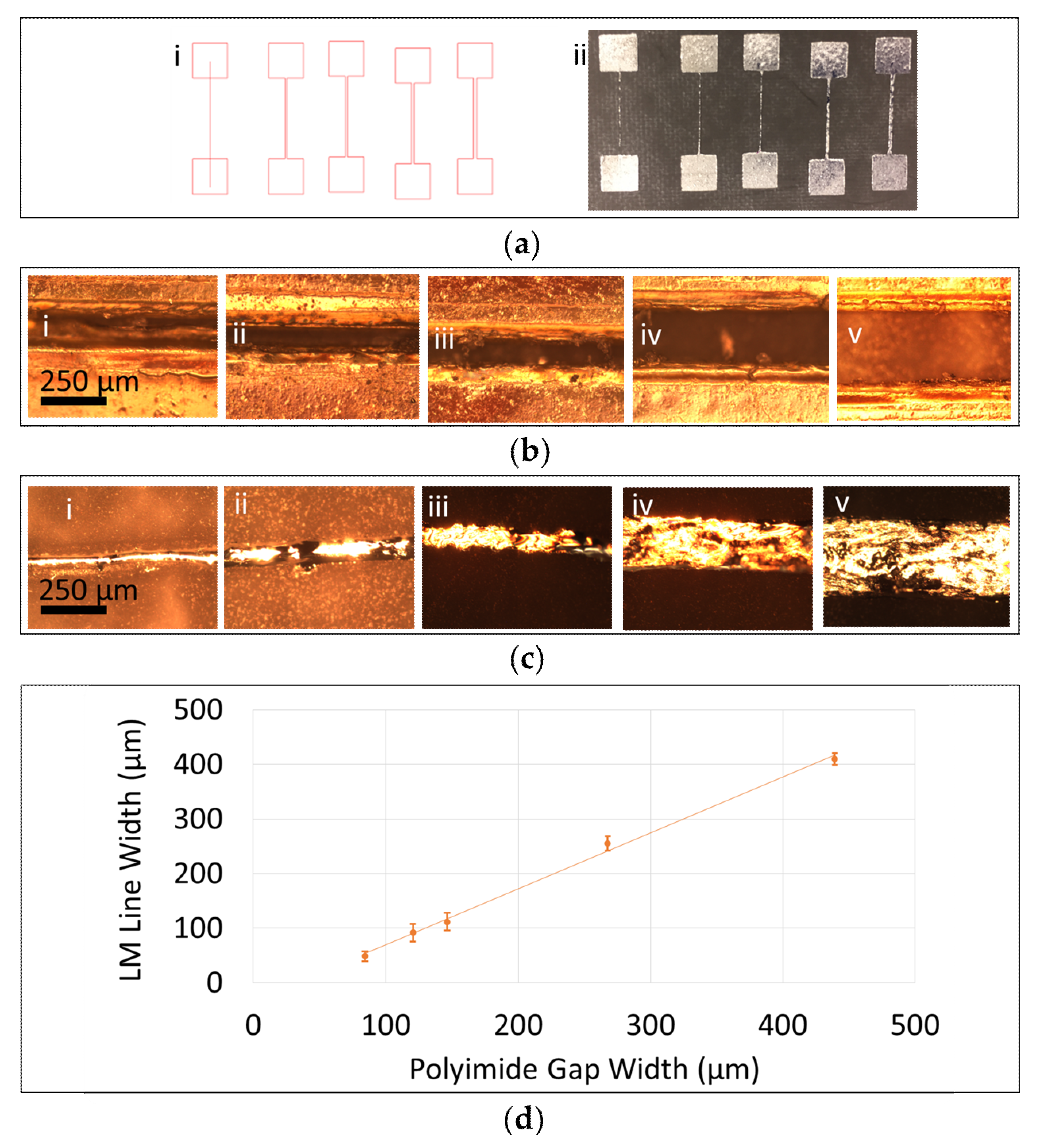
3.3. Minimum Feature Size of Sprayed LM

LM lines were patterned using a polyimide mask, as described in Section 2, to determine the minimum feature size that can be achieved. The spraying conditions were optimized to produce the smallest possible droplet size of sprayed LM, thus a higher pressure of 140 PSI (965.2 kPa) was used for this experiment, along with a spraying time of 3 s and a distance of 10 cm between the sprayer and the substrate. Figure 9a shows the patterns of the sprayed LM. Figure 9b shows microscopic images of the polyimide tape before spraying the LM. The smallest gap in the polyimide tape was 84 µm wide. Figure 9c shows microscopic images of the sprayed LM after removing the polyimide mask. The smallest feature size was 48 µm, obtained using the mask with the 84-μm-wide gaps. Figure 9d shows the LM line widths vs. the width of the gaps in the polyimide mask. The measured line widths in the polyimide mask are larger than the measured LM line widths. This difference may be from adhesive residue left behind after the polyimide tape was cut. The polyimide edges had dangling adhesive residue that remained after the polyimide cut by the craft cutter was removed.

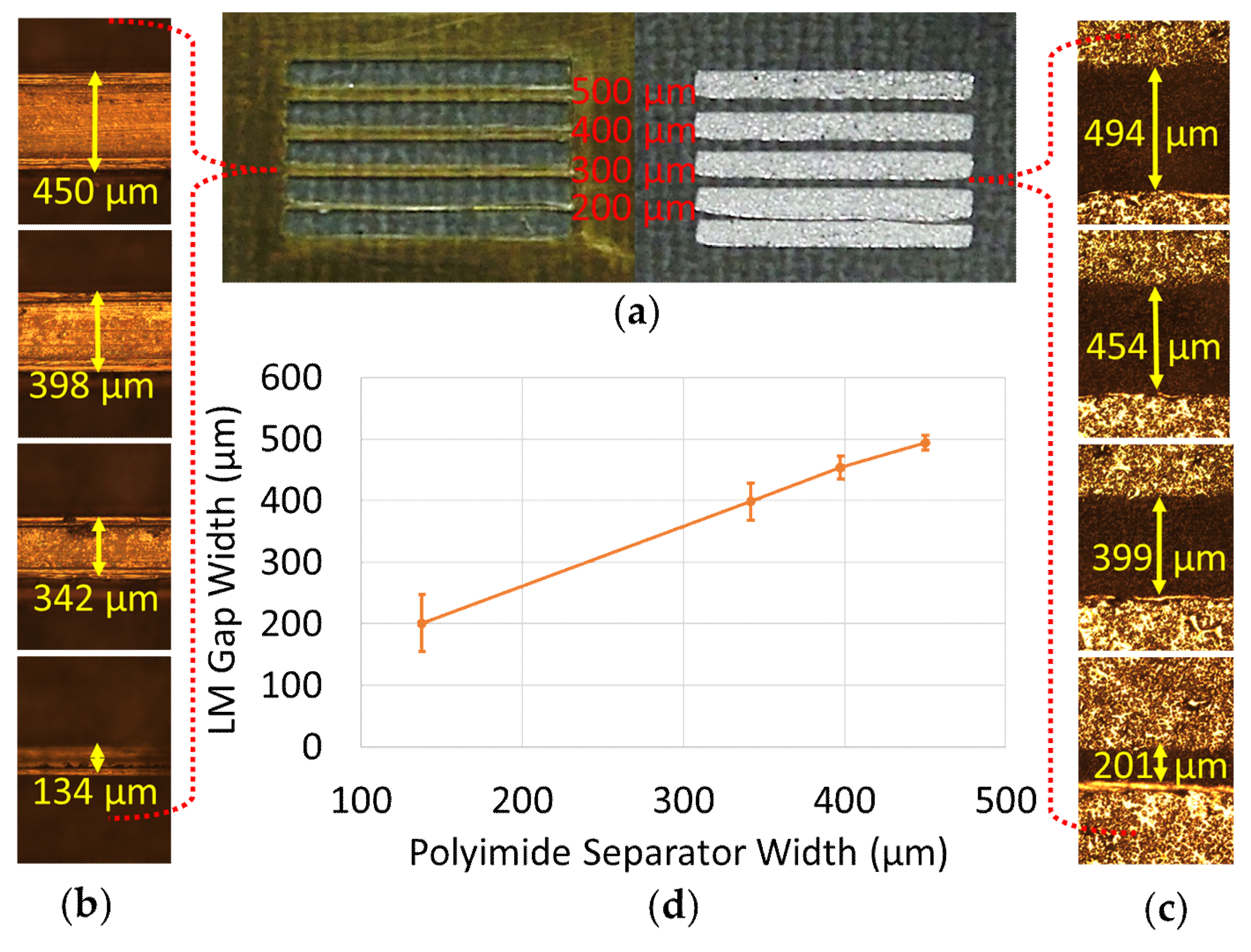
3.4. Minimum LM-Gap Size

The gap size between sprayed LM patterns was determined by the width of a “separator” pattern in the polyimide mask. Figure 10a shows images for the polyimide separators before spraying LM, and for the sprayed LM gaps after removing the mask. Figure 10b shows microscopic images of the separators in the polyimide mask. Figure 10c shows microscopic images of the gaps between sprayed LM lines. Figure 10d shows the measured gap width between sprayed LM lines vs. the measured width of polyimide separators (before spraying LM). After spraying LM, the gaps were found to be wider than the measured separator width in the polyimide mask. This indicates good adhesion between the mask and the substrate, which was an issue in the other sprayed-LM work; it was reported that the mask has to be held tightly to the substrate to prevent LM sprayed particles from leaking below the mask and eventually distorting the edges [9,14,15,16]. The larger LM gaps also may be from the presence of residual adhesive from the polyimide mask. The minimum obtained gap was 201 µm after spraying LM.

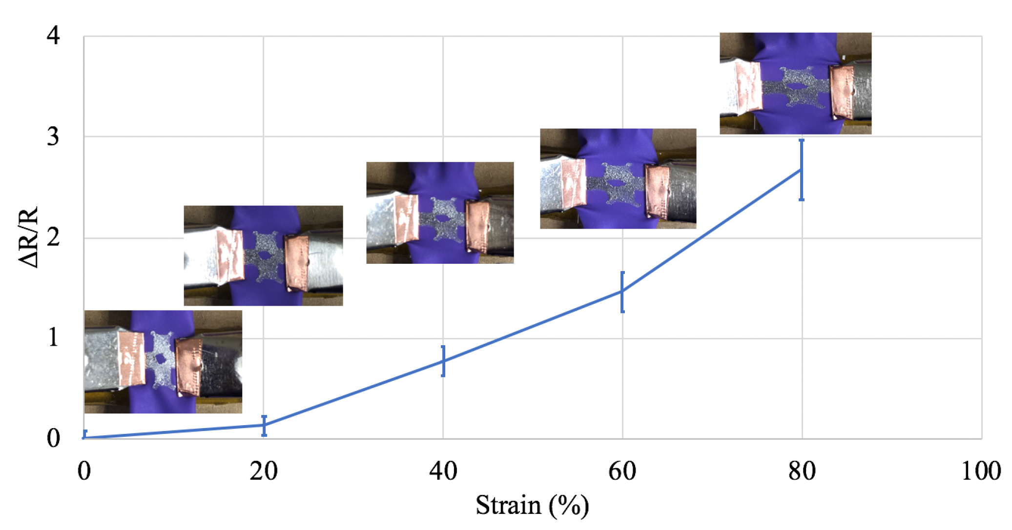
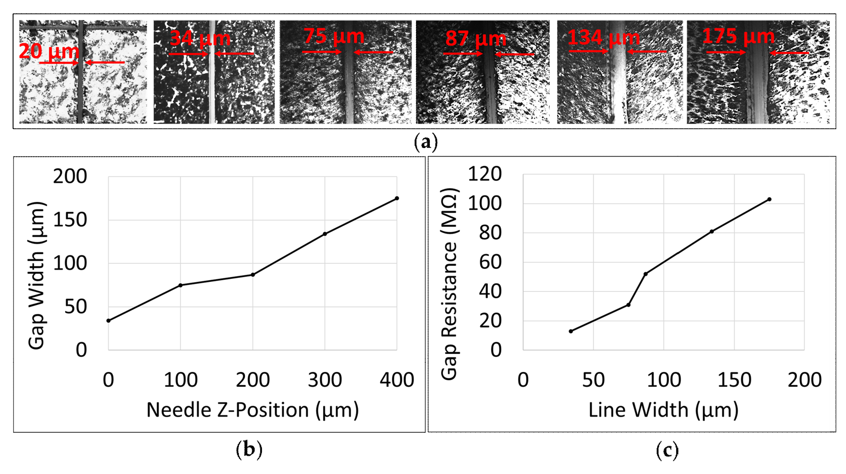
3.5. Subtractive LM Patterning by Physical Scraping

Subtractive patterning of LM can increase the resolution of gaps patterned in the sprayed LM film. In this process, a homogenous LM film was sprayed onto a PDMS substrate. Then, a 30-gauge sharp-edged needle was mounted to the print-head of an Inkredible 3D printer (Figure 11). A single-layer pattern was uploaded to the printer. The printer moves the needle along the pattern, scraping the sprayed LM film. Figure 12a shows microscopic images for the gaps in the LM created by the scraping. This subtractive method created a minimum gap size of 34 µm. Figure 12b shows the variation of the needle z position versus the scraped gap width. The z = 0 position corresponds to the needle position that created the minimum gap size (34 μm) in the LM using the 34-gauge needle. The height between the substrate and the tip of the needle was adjusted to scrape the sprayed LM layer without visibly damaging the PDMS substrate. As the z position increases, the needle is pushed further into the substrate, creating a wider gap. As the gap increases, the measured resistance across the LM gap also increases (Figure 12c). The measured resistance of 1 cm2 of sprayed LM was 240 mΩ before scraping. The measured resistance of the smallest scraped gap, 34 µm, was 14 MΩ. The minimum resistance of the scraped gaps (Figure 12) is six orders of magnitude higher than the resistance of LM lines. This provides enough contrast between conductive and insulating patterns for circuits operating from DC to approximately 2 GHz. For higher-frequency applications, gaps of less than 100 µm can have significant capacitive coupling. Supplementary Figure S1 shows the simulated insertion loss of a transmission line with capacitive coupling.

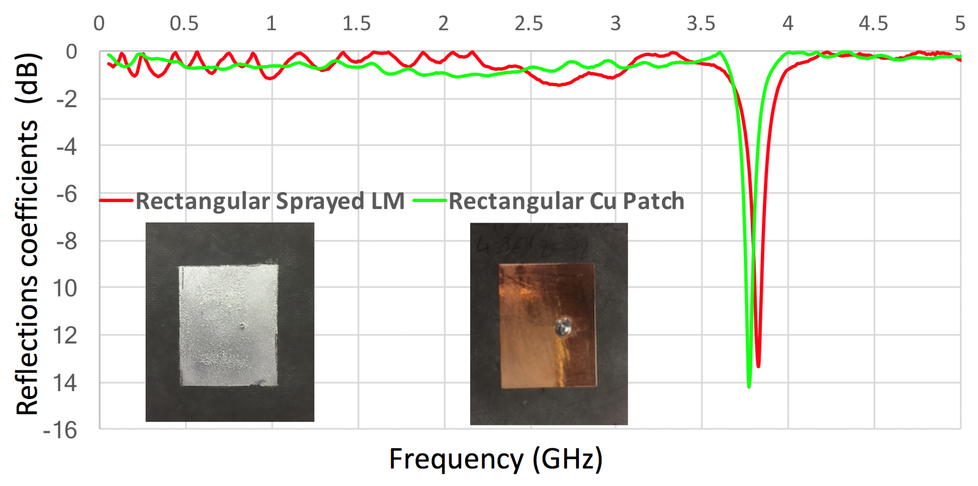
3.6. Sprayed LM Patch Antenna

A coaxially-fed rectangular patch antenna was designed to radiate at 3.8 GHz using dimensions of 31.5 mm × 25.4 mm. First, the antenna was implemented and measured using copper (Cu), then by a sprayed LM patch using a polyimide mask; both were fabricated on Rogers Duroid 5880 substrate. Figure 13 shows a good match between the reflection coefficients of the Cu and LM patch antennas, as both resonate around 3.8 GHz. Similar performance of LM and Cu antennas has been reported in literature. An unstretched LM loop antenna had a radiation efficiency of 98% [23]. The gain of an LM monopole antenna was 5.10 to 5.26 dBi [24], matching the gain of a standard monopole (5.17 dBi). An embedded vascular LM dipole antenna had nearly identical radiation patterns as a Cu dipole antenna [25], and a helical LM antenna had the same gain as the Cu version of the antenna [26].

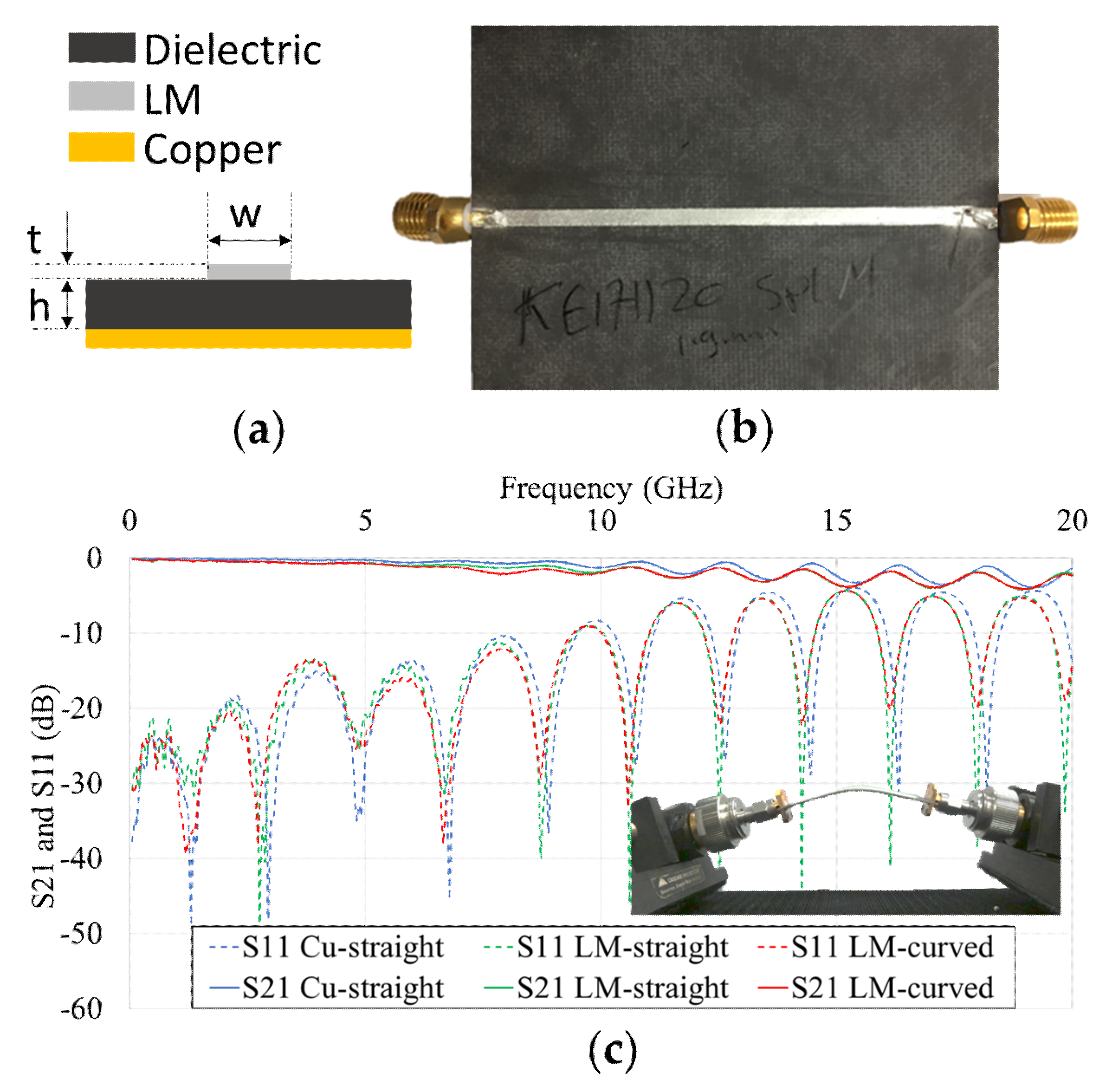
3.7. Sprayed LM Transmission Line

Table 1 shows the dimensions and parameters of the sprayed LM transmission line (TL). The TL was designed for a 50-Ω impedance. First, the TL was implemented and measured using a standard Cu trace, then using a sprayed LM trace made with a polyimide mask. Figure 14a shows a schematic image for the sideview of the TL. Figure 14b shows an image for the sprayed LM TL. Figure 14c shows the measured insertion loss and return loss of the Cu and LM TLs. For both of the LM and Cu TLs, the insertion loss (S21) is less than 5 dB up to 20 GHz, and the return loss (S11) is greater than 10 dB up to 10 GHz. Therefore, it is concluded that there is an acceptable match between LM and Cu TL performances. Bending the LM transmission line at a radius of curvature of 8 cm did not significantly affect the insertion loss or the reflection coefficient. The bending radius was limited by the characterization setup and connectors rather than the performance of the sprayed LM.
The Cu TL was fabricated using copper tape; the material cost for the TL is estimated to be $0.046. The LM transmission line was fabricated using a polyimide mask (material cost of approximately $0.01) and the amount of LM used to create the transmission line was approximately 0.05 mL (material cost of approximately $0.062). Although the materials cost of the LM TL is more expensive than the Cu TL, it is still inexpensive. The sprayed LM has the additional advantage of compatibility with flexible and stretchable substrates.

4. Discussion

This work improves upon previous efforts in atomizing LM. Although spraying LM is a quick procedure that consumes small amounts of LM to create conductive patterns, the use of micromachined shadow masks [14] to pattern the LM increases the cost and time of fabrication. The techniques demonstrated here address these issues using polyimide tape and PUA masks. For both methods described in this paper, the cost of materials is less than $1 to implement a sub-millimeter mask, and the fabrication time is less than 5 min. A commercially available craft cutter (Silhouette, approximately $110) was used to cut the polyimide tape to create masks, whilst a commercially available UV light (approximately $30) was used to cure the PUA for the UV-curable masks.
A problem that has been associated with the spraying of LM was the smearing of LM below the edges of the stencil masks [14,15,16]. This issue has been resolved by using masks made of polyimide tape and PUA membranes, which conformally adhere to the surface of the substrate. The minimum feature sizes reported in previous efforts were 500 µm [14], 200 µm [15], and 234 µm [16], produced using a micromachined mask, screen mesh, and a vinyl mask, respectively. This paper demonstrated a feature size of 150 µm using the PUA mask, and a line width below 50 µm using the polyimide mask. The reported minimum spacing between patterns in a previous study [16] was 75 µm, compared to 34 µm in this paper, obtained by scraping the sprayed LM with a needle. Introducing gaps at this resolution can be useful for terahertz circuits, although this is beyond the scope of this work due to limitations on the available equipment. Moreover, the scraping technique can be automated by mounting the needle to the printhead of a 3D printer, as illustrated in Figure 11. In addition to the transmission line and antenna demonstrated here, this method of spraying LM was used to create LM contacts for a graphene transistor [27].

5. Conclusions

Various fabrication techniques for patterning sprayed LM on flexible and rigid substrates were demonstrated. The effects of the spraying time, distance, and pressure on the obtained LM thickness and conductivity were characterized. Optimal spraying conditions were used to achieve a minimum feature size of 48 µm in sprayed LM, and a minimum gap width of 201 µm between LM lines. Physical scraping of the sprayed LM can reduce the minimum gap width to 34 µm. Polyimide and UV-curable masks were used to pattern the sprayed LM. Both masking techniques are compatible with flexible and curved substrates. Thus, this sprayed LM fabrication process can be used for low-cost rapid prototyping of flexible and conformal communication devices and sensors. As a proof of concept, a patch antenna and transmission line were fabricated using sprayed LM. The performance of the sprayed LM devices were very similar to the reference copper versions.

Supplementary Materials

The following are available online at https://www.mdpi.com/2076-3417/9/8/1565/s1, Figure S1: Simulation results for the insertion loss of as transmission line with a capacitive coupling; Figure S2: Images of the droplets sprayed at various pressures measured by a laser scanning microscope.

Author Contributions

Conceptualization, S.S. and A.T.O.; data curation, K.S.E., S.S., and T.K.A.; formal analysis, K.S.E. and S.S.; investigation, K.S.E. and S.S.; methodology, K.S.E. and S.S.; project administration, S.S. and A.T.O.; resources, S.S., W.A.S., and A.T.O.; supervision, W.A.S. and A.T.O.; validation, S.S. and A.T.O.; visualization, K.S.E., S.S., and T.K.A.; writing—original draft, K.S.E. and S.S.; writing—review and editing, K.S.E., S.S., W.A.S., and A.T.O.

Funding

Research supported in part by the National Science Foundation, award number ECCS-1546980.

Conflicts of Interest

The authors declare no conflict of interest.

References

  1. Huang, S.; Liu, Y.; Zhao, Y.; Ren, Z.; Guo, C.F. Flexible electronics: Stretchable electrodes and their future. Adv. Funct. Mater. 2019, 29, 1805924. [Google Scholar] [CrossRef]
  2. Liu, Y.; Wang, H.; Zhao, W.; Zhang, M.; Qin, H.; Xie, Y. Flexible, stretchable sensors for wearable health monitoring: Sensing mechanisms, materials, fabrication strategies and features. Sensors 2018, 18, 645. [Google Scholar] [CrossRef] [PubMed]
  3. Rajan, K.; Garofalo, E.; Chiolerio, A. Wearable intrinsically soft, stretchable, flexible devices for memories and computing. Sensors 2018, 18, 367. [Google Scholar] [CrossRef] [PubMed]
  4. Zhu, J.; Cheng, H. Recent development of flexible and stretchable antennas for bio-integrated electronics. Sensors 2018, 18, 4364. [Google Scholar] [CrossRef] [PubMed]
  5. Koo, J.H.; Kim, D.C.; Shim, H.J.; Kim, T.H.; Kim, D.H. Flexible and stretchable smart display: Materials, fabrication, device design, and system integration. Adv. Funct. Mater. 2018, 28, 1801834. [Google Scholar] [CrossRef]
  6. Park, M.; Im, J.; Shin, M.; Min, Y.; Park, J.; Cho, H.; Park, S.; Shim, M.-B.; Jeon, S.; Chung, D.-Y.; et al. Highly stretchable electric circuits from a composite material of silver nanoparticles and elastomeric fibres. Nat. Nanotechnol. 2012, 7, 803–809. [Google Scholar] [CrossRef] [PubMed]
  7. Zuazola, I.J.G.; Sharma, A.; Batchelor, J.C.; Angulo, I.; Perallos, A.; Elmirghani, J.M.H. Sprayed antenna on cans for WLAN-RFID tags. Microw. Opt. Technol. Lett. 2013, 55, 773–775. [Google Scholar] [CrossRef]
  8. Shen, W.; Li, M.; Wang, B.; Liu, J.; Li, Z.; Jiang, L.; Song, Y. Hierarchical optical antenna: Gold nanoparticle-modified photonic crystal for highly-sensitive label-free DNA detection. J. Mater. Chem. 2012, 22, 8127–8133. [Google Scholar] [CrossRef]
  9. Guo, C.; Yu, Y.; Liu, J. Rapidly patterning conductive components on skin substrates as physiological testing devices via liquid metal spraying and pre-designed mask. J. Mater. Chem. B 2014, 2, 5739–5745. [Google Scholar] [CrossRef]
  10. Varga, M.; Ladd, C.; Ma, S.; Holbery, J.; Tröster, G. On-skin liquid metal inertial sensor. Lab Chip 2017, 17, 3272–3278. [Google Scholar] [CrossRef]
  11. Arumugam, S.; Li, Y.; Senthilarasu, S.; Torah, R.; Kanibolotsky, A.L.; Inigo, A.R.; Skabara, P.J.; Beeby, S.P. Fully spray-coated organic solar cells on woven polyester cotton fabrics for wearable energy harvesting applications. J. Mater. Chem. A 2016, 4, 5561–5568. [Google Scholar] [CrossRef]
  12. Kang, J.S.; Kim, H.S.; Ryu, J.; Thomas Hahn, H.; Jang, S.; Joung, J.W. Inkjet printed electronics using copper nanoparticle ink. J. Mater. Sci. Mater. Electron. 2010, 21, 1213–1220. [Google Scholar] [CrossRef]
  13. Hösel, M.; Krebs, F.C. Large-scale roll-to-roll photonic sintering of flexo printed silver nanoparticle electrodes. J. Mater. Chem. 2012, 22, 15683–15688. [Google Scholar] [CrossRef]
  14. Zhang, Q.; Gao, Y.; Liu, J. Atomized spraying of liquid metal droplets on desired substrate surfaces as a generalized way for ubiquitous printed electronics. Appl. Phys. A Mater. Sci. Process. 2014, 116, 1091–1097. [Google Scholar] [CrossRef]
  15. Jeong, S.H.; Hjort, K.; Wu, Z. Tape transfer atomization patterning of liquid alloys for microfluidic stretchable wireless power transfer. Sci. Rep. 2015, 5, 8419. [Google Scholar] [CrossRef]
  16. Wang, L.; Liu, J. Pressured liquid metal screen printing for rapid manufacture of high resolution electronic patterns. RSC Adv. 2015, 5, 57686–57691. [Google Scholar] [CrossRef]
  17. Liu, T.; Sen, P.; Kim, C.J. Characterization of nontoxic liquid-metal alloy Galinstan for applications in microdevices. J. Microelectromech. Syst. 2012, 21, 443–450. [Google Scholar] [CrossRef]
  18. Yuen, P.K.; Goral, V.N. Low-cost rapid prototyping of flexible microfluidic devices using a desktop digital craft cutter. Lab Chip 2010, 10, 384–387. [Google Scholar] [CrossRef] [PubMed]
  19. Khondoker, M.A.H.; Sameoto, D. Fabrication methods and applications of microstructured gallium based liquid metal alloys. Smart Mater. Struct. 2016, 25, 093001. [Google Scholar] [CrossRef]
  20. Wu, H.; Kong, D.; Ruan, Z.; Hsu, P.C.; Wang, S.; Yu, Z.; Carney, T.J.; Hu, L.; Fan, S.; Cui, Y. A transparent electrode based on a metal nanotrough network. Nat. Nanotechnol. 2013, 8, 421–425. [Google Scholar] [CrossRef] [PubMed]
  21. Lee, H.; Hong, S.; Lee, J.; Suh, Y.D.; Kwon, J.; Moon, H.; Kim, H.; Yeo, J.; Ko, S.H. Highly stretchable and transparent supercapacitor by Ag–Au Core–Shell nanowire network with high electrochemical stability. ACS Appl. Mater. Interfaces 2016, 8, 15449–15458. [Google Scholar] [CrossRef] [PubMed]
  22. Kim, J.H.; Hong, S.H.; Seong, K.D.; Seo, S. Fabrication of organic thin-film transistors on three-dimensional substrates using free-standing polymeric masks based on soft lithography. Adv. Funct. Mater. 2014, 24, 2404–2408. [Google Scholar] [CrossRef]
  23. Cheng, S.; Rydberg, A.; Hjort, K.; Wu, Z. Liquid metal stretchable unbalanced loop antenna. Appl. Phys. Lett. 2009, 94, 92–95. [Google Scholar] [CrossRef]
  24. Morishita, A.M.; Kitamura, C.K.Y.; Shiroma, W.A.; Ohta, A.T. Two-octave tunable liquid-metal monopole antenna. Electron. Lett. 2013, 50, 19–20. [Google Scholar] [CrossRef]
  25. Hartl, D.J.; Frank, G.J.; Huff, G.H.; Baur, J.W. A liquid metal-based structurally embedded vascular antenna: I. Concept and multiphysical modeling. Smart Mater. Struct. 2017, 26, 025001. [Google Scholar] [CrossRef]
  26. Zhou, Y.; Fang, S.; Liu, H.; Fu, S. A Liquid metal conical helical antenna for circular polarization-reconfigurable antenna. Int. J. Antennas Propag. 2016, 2016, 3782373. [Google Scholar] [CrossRef]
  27. Melcher, J.; Elassy, K.; Ordonez, R.; Hayashi, C.; Ohta, A.; Garmire, D.; Melcher, J.L.; Elassy, K.S.; Ordonez, R.C.; Hayashi, C.; et al. Spray-on liquid-metal electrodes for graphene field-effect transistors. Micromachines 2019, 10, 54. [Google Scholar] [CrossRef] [PubMed]
Figure 1. Schematic illustration of liquid metal (LM) spraying process.
Applsci 09 01565 g001
Figure 2. Characterization of sprayed LM thickness under various spraying pressures: LM thickness when it is sprayed from a nozzle (a) 5 cm and (b) 10 cm away from the substrate.
Applsci 09 01565 g002
Figure 3. Characterization of sprayed LM line thickness when sprayed onto a substrate 3 cm, 5 cm, and 10 cm away from the nozzle for 1 s, 3 s, and 5 s. The spraying pressure is varied from (a) 100 kPa, (b) 150 kPa, and (c) 200 kPa.
Applsci 09 01565 g003
Figure 4. Conductivity of LM film sprayed at a distance of (a) 5 cm and (b) 10 cm from the substrate for 1 s, 3 s, and 5 s, under various spraying pressures.
Applsci 09 01565 g004
Figure 5. Change in normalized measured resistance versus uniaxial strain for a sprayed LM pattern on a stretchable nitrile surface.
Applsci 09 01565 g005
Figure 6. Illustration of the fabrication process for UV-curable polymeric membrane.
Applsci 09 01565 g006
Figure 7. (a) UV-curable polymeric membrane (2 cm × 2 cm) and (b) the membrane attached to a glass substrate. (c) Galinstan was sprayed on the polymer membrane and (d) the LM dots pattern remained on the glass substrate after peeling off the membrane.
Applsci 09 01565 g007
Figure 8. (a) Optical image of 150-µm holes LM pattern by spray printing with polymeric membrane mask. Other patterns have been fabricated, (b) a letter “C” and (c) a short electrode line.
Applsci 09 01565 g008
Figure 9. Measurement of sprayed LM line width. (a.i) Polyimide mask layout. (a.ii) Sprayed LM after removing the polyimide mask. (b) Images of the polyimide mask, with the cut gaps running through the center of the photos. (c) Images of the sprayed LM lines. (d) Measured LM line width vs. the width of the gap in the polyimide mask.
Applsci 09 01565 g009
Figure 10. Measurement of gap width between sprayed LM. (a) Images of the polyimide mask and the sprayed LM. (b) Images of the polyimide mask, with the separator running through the center of the photos. (c) Images of the gaps between sprayed LM. (d) Measured gap width between sprayed LM lines vs. the polyimide separator width.
Applsci 09 01565 g010
Figure 11. Set-up for scraping sprayed LM: (a) Schematic of the set-up, (b) photo of the Inkredible 3D Bioprinter, and 30-gauge needle for physically scraping the liquid metal film.
Applsci 09 01565 g011
Figure 12. Characterization of scraped LM. (a) Images of the scraped LM with different gap widths. (b) Gap width in the sprayed LM vs. the z-position of the needle. (c) Resistance measured across the gap vs. gap width.
Applsci 09 01565 g012
Figure 13. Reflection coefficient of Cu and LM rectangular patch antennas.
Applsci 09 01565 g013
Figure 14. Sprayed-LM transmission line: (a) cross-section, (b) photo of the implemented sprayed-LM TL, and (c) measured insertion loss (S21) and return loss (S11) of a straight Cu TL and a straight and curved sprayed LM TL.
Applsci 09 01565 g014
Table 1. TL dimensions and parameters.
ParameterValue
Zo (target impedance)50 Ω
t (trace thickness)0.06 mm
h (dielectric thickness)0.787 mm
Ɛr (relative dielectric constant)2.2
w (trace width)1.9 mm

