1. Introduction
In recent decades, the short pulsed laser has been widely utilized in the fields of production, medical, detection and communication, and so on, as the ultra-short pulse laser technology develops rapidly [
1,
2]. Among various types of lasers, semiconductor lasers are suitable for producing ultra-short optical pulses because of their large gain bandwidth, small volume and high modulation efficiency [
3,
4,
5]. The direct modulation technology of the semiconductor laser is mainly used to generate optical pulses, which has the advantages of simple operation, low cost, and mature technology. However, in order to achieve high-speed modulation in the optical communication system, the driving current is higher than the threshold current. As a result, the output pulse width is similar to that of the driving current, and the pulse power is proportional to the amplitude of the driving current. There is a trade-off between the high extinction ratio and the short pulse width [
6,
7,
8,
9].
Gain-switched technology is another direct modulation method to generate short optical pulses by using the relaxation oscillation of the semiconductor laser, and it has been widespread use because of its compact structure, stable performance, and flexible setting. The relaxation oscillation is a transient phenomenon in lasers, which refers to a series of gradually decaying spike pulse sequence attributing to the self-oscillation before the laser achieves stabilized output. The standard gain-switched arrangement is to drive a laser, biased below the threshold. The idea is to excite the first spike of relaxation oscillation, and terminate the electrical pulse before the onset of the second optical spike, resulting in a short light pulse. Repeat this process to achieve a pulse sequence on the order of picosecond [
10,
11]. Compared with other pulse generation methods, this idea has an advantage that a simple driving circuit can be used to generate an ultra-short optical pulse, and the output pulse width is much smaller than the modulation current pulse. Theoretical analysis indicates that the photon lifetime of a typical semiconductor laser is 2~3 picosecond, so a ten picosecond laser pulse can be produced theoretically by using a hundred picosecond current pulse in the process of gain switching [
12,
13].
The characterization of the gain-switched semiconductor laser pulse is also affected by the modulation parameters. In Reference [
14], it has been verified that using the rectangular wave modulation can achieve high pulse power and a small tail, compared to the sine and triangle waves with the same magnitude. Besides, the peak power of the output pulse increases with the increase of rectangular modulated signal width, and finally reaches saturation, according to the study on relaxation oscillation [
15]. According to the typical study for the gain switching process of the semiconductor laser, the peak power and width of the output pulses are mainly determined by the accumulation speed after the carrier density reaches the threshold. Based on this theory, a step-pulse modulated signal is proposed on more peak power improvements. In this paper, we primarily focus on the effect of step modulated signal’s variation on gain-switched semiconductor lasers, demonstrate the feasibility of the proposed methods and find the best modulation parameter. Moreover, we get a function between the amplitude of the signal and the pulse width by curve fitting technic. The simulation results show that the proposed scheme can further compress the laser pulse width and increase the amplitude value. The final simulation results show that the proposed method can further compress the laser pulse width and increase the amplitude value.
2. Step Modulation Principles
The relaxation oscillation process can be set up by the rate equations, in which the steady and dynamic characteristics of a semiconductor laser can be described efficiently and accurately with the following single mode rate equations [
16,
17,
18]:
The output power is given in terms of the photon density [
19]:
where
N and
S are the carrier density and photon density,
J is the injected current, other parameters and their typical values are shown in
Table 1.
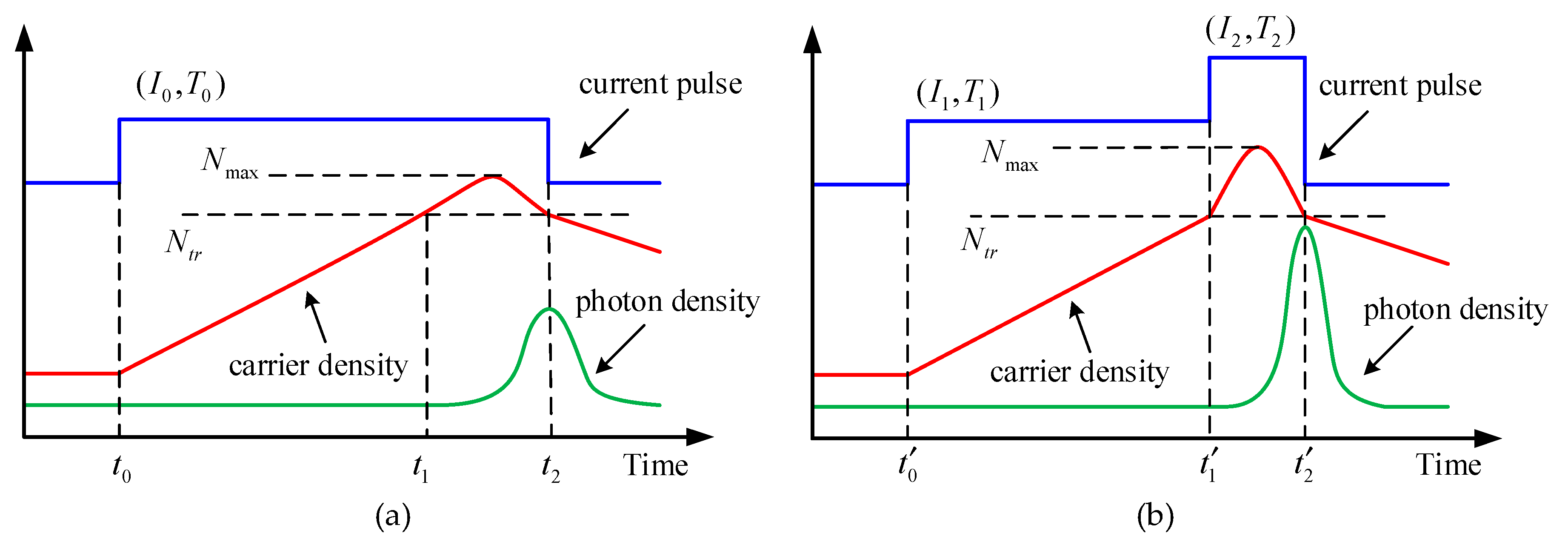
Figure 1 shows the evolution in the carrier and photon densities during a gain switch cycle, assuming that the bias current is 0 and that the initial photon density in the laser can be ignored. A rectangular wave modulation process is given in
Figure 1a: At time
, a current pulse is applied to a laser with the amplitude of
and pulse width of
. The initial rate of increase in photon density is very low, due to its low initial value. Without being significantly consumed by stimulated emission, injected electrons rapidly build the carrier density up to threshold
at time
. After that, the population inversion can be achieved, and the laser begins to emit the light pulse. When the stimulated emission begins to consume the carrier significantly, the population inversion reaches the maximum value
. With the generation of laser pulses, the carrier density drops to the threshold at time
, at which point the output pulse power reaches its peak value. At this time, the current should be terminated quickly to restrain the secondary oscillation. Therefore, to form a single pulse output with high peak power, the rectangular current pulse must be terminated for the first time when the carrier density drops to the steady-state threshold [
20].
The above analysis shows that, before the carrier density reaches the threshold, the photons are mainly generated by the spontaneous emission of the laser. Afterward, the carriers injected into the laser begin to be converted into stimulated emission photons. The peak reversal rate of carrier density given in the Reference [
21] is
, and with increasing
R, the peak power of the output pulse increased while the full width at half maxima (FWHM) decreased. Therefore, if we can increase the modulation current suddenly at the moment when the carrier density reaches the threshold, the peak reversal rate can be increased, and the optical pulse with higher power and shorter width will be obtained. To do this a step-pulse modulated signal is designed, as shown in
Figure 1b, in which the amplitude of the first modulation current is
, the pulse width is
, the second modulation current amplitude is
, and the pulse width is
.
Figure 1b shows the step-pulse modulation process: When the current is injected at time
, the carrier density increases gradually and achieves the threshold at time
; then the increase rate of carrier density is obviously improved and the peak power of output pulse increases as the modulation current becomes larger; finally the peak power reaches a maximum when the carrier density drops to the threshold at time
.
According to the process of step-pulse modulation process, the primary function of the first-stage modulation current (FSMC) is to accumulate the carrier, while the output pulse characteristic is mainly affected by the second-stage modulation current (SSMC). So when
, the carrier density in the laser does not reach the threshold after the end of the FSMC, until the SSMC has been injected for a period. Thus, the SSMC is not fully utilized for not the entire injected carrier is converted into the stimulated photon. When
, the laser has entered the stimulated emission state at the end of the FSMC, and the SSMC will not entirely increase the carrier injection rate. As a result, combined with the studies of Reference [
22], a simple design of the FSMC is
, that is to say, the semiconductor laser works stably at the threshold level before the SSMC begins.
3. Step Modulation Simulation and Discussion
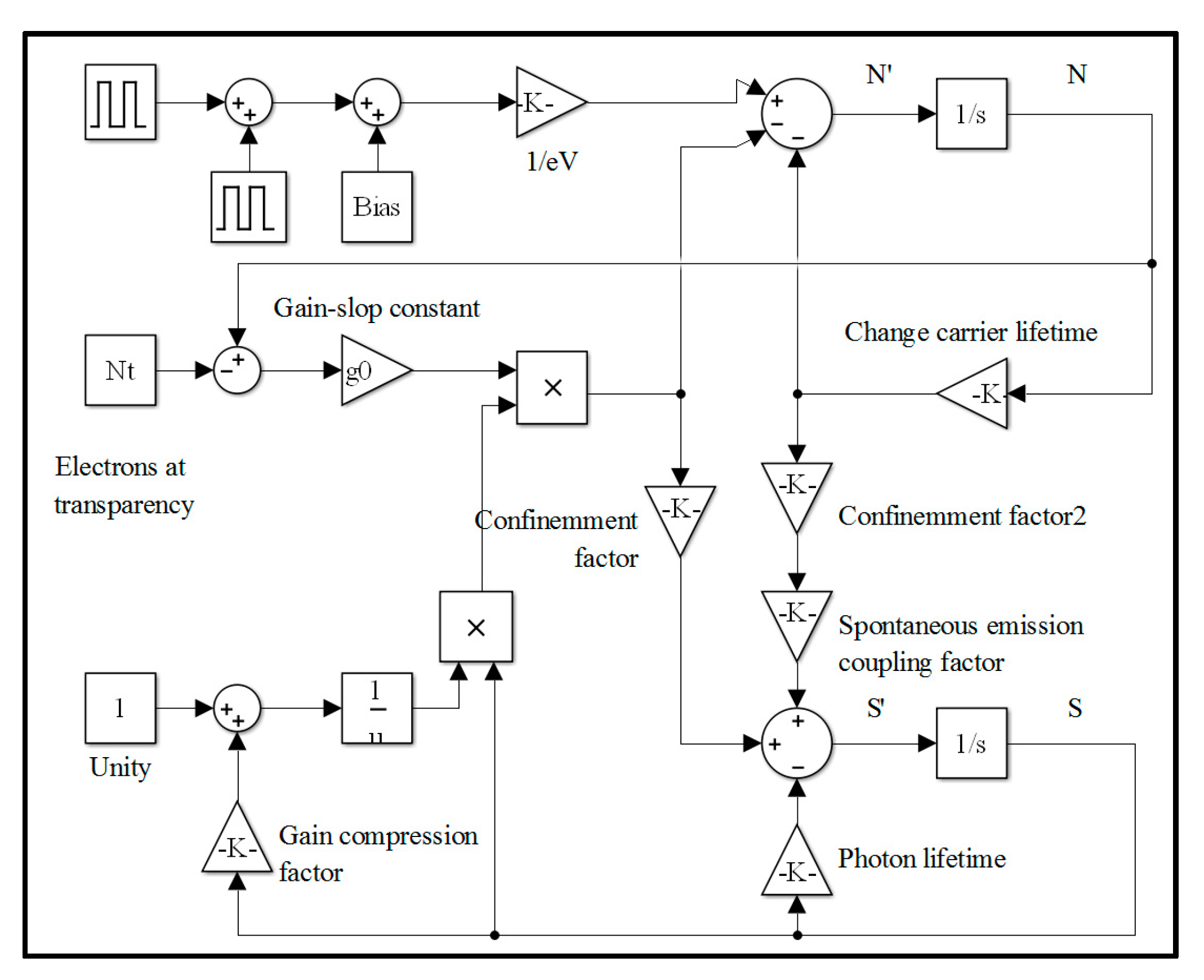
In order to analyze the effect of the parameter setting of the second stage modulated signal on the output light pulse, we establish the simulation models of single mode rate equations (Equations (1) and (2)) by SIMULINK, which is a visual simulation of MATLAB. To simulate the variation of the output pulse, we excite the semiconductor laser with a single current pulse. The amplitude of the first-stage modulation current is set to
mA, and the width is
ns, which is equal to the time of carrier density reaching the threshold for the first time. The bias current is set to 0 mA in order to get a high extinction ratio [
23]. The block diagram of step modulation simulation is shown in
Figure 2.
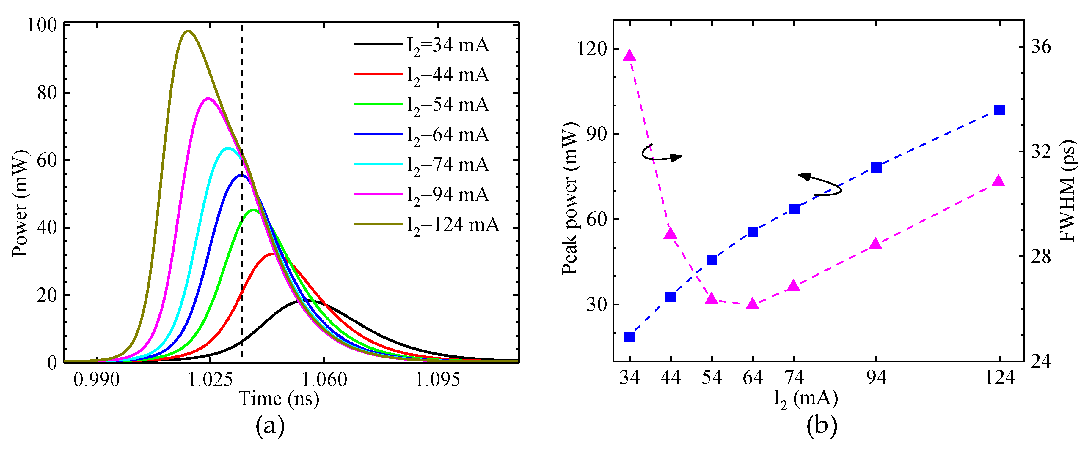
Figure 3 shows the simulation results of output pulses at different
when the
ps. From
Figure 3a, in which the dotted line corresponds to the end time of the modulation current, it is directly seen that with the increase of
, the rising edge of the output pulse becomes steep, the peak time is short, and the peak power is high. However, the pulse width decreases at first and then increases, as shown in
Figure 3b. If
mA, the step modulated signal can change into a rectangular modulated wave, it is clearly seen that using the step modulation can cause pulse energy increase and pulse duration decrease. When
mA, the output power reaches the maximum value at the time corresponding to the dotted line, also, the FWHM pulse width is smallest. When
mA, the peak pulse power lags behind the end time of current and the output pulse rise time is short, that is because the carrier density has not fallen to the threshold before the end of the current, even if terminating the injection current there will be excess carriers converted into photons. Therefore, as the accumulation rate of carriers increases proportionally to the
, the output pulse becomes narrow, and the peak power becomes large. When
mA, the output pulse has reached the peak before the current is terminated, and the pulse tail will appear with the injection of excess carriers. The bigger is the
, and the more serious is the tailing. Thus, the conclusion one is: When
is certain,
should be set to meet the condition–the output power reaches the maximum time is equal to the current termination time, in order to minimize the width of the output pulse.
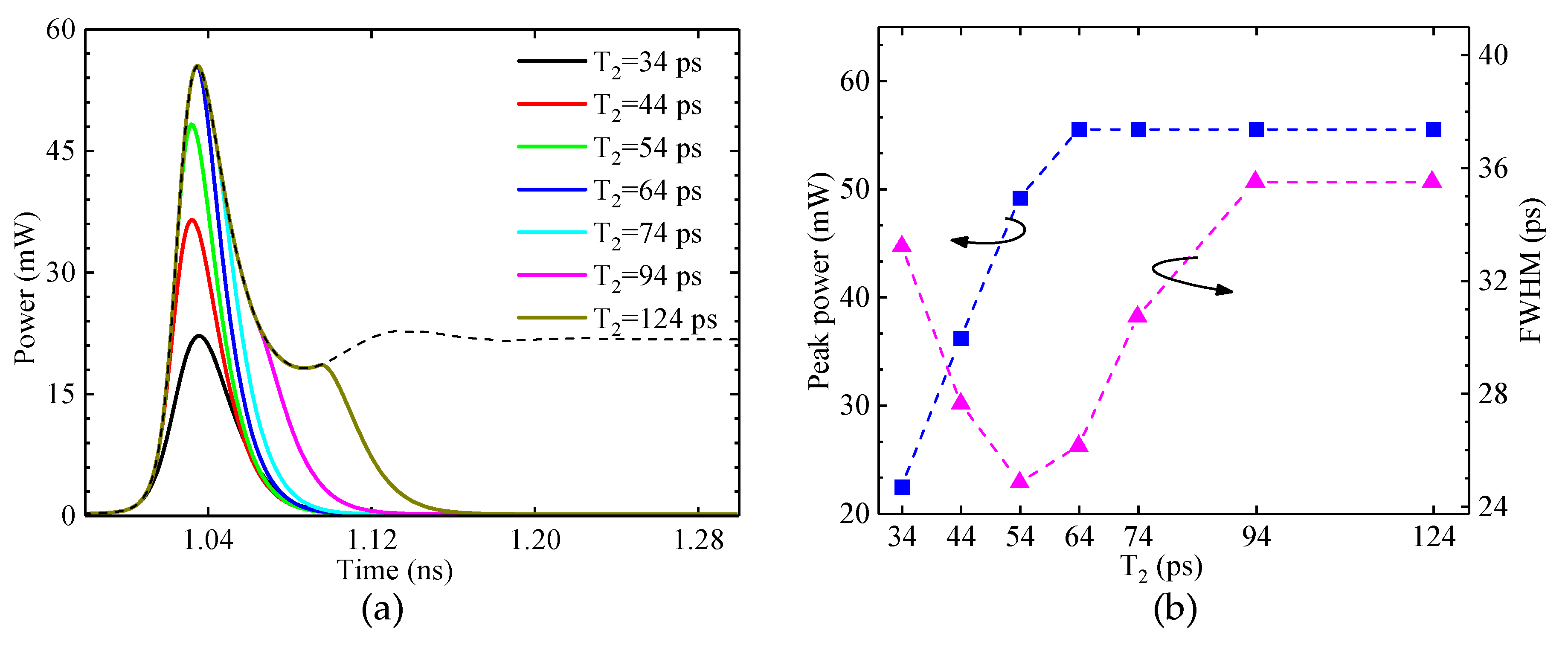
The simulation results of the output pulses at different
are shown in
Figure 4, in which the
mA. From
Figure 4a, it is directly seen that the output pulses have the similar front-end when fixing
, and the peak power increases with
until it reaches saturation. Similarly, with the increase of
, the changing rule of FWHM is first reduced and then increased, before reaching a steady value, as shown in
Figure 4b. When
ps, the peak power of output pulse reaches the maximum for the first time, which means the carrier density drops to the threshold at the moment of cutting the driving current completely. When
ps, the photon density is still on the rise, so the extended modulation time can increase the cumulative number of carriers and thus enhance the peak power. In such a situation, if
is small, the gain coefficient changes greatly with
and the accumulation rate of the photon is fast, which leads to the FWHM becomes small; else, the front-end of output pulses change slowly, and the FWHM becomes big. When
ps, the peak power does not change with the increase of
because of the photon density saturation phenomenon. However, the extension of the modulation time causes the post-stage oscillation to appear, and the pulse tail becomes worse. The fall time are 28.9 ps (64 mA), 32.7 ps (74 mA), 49.2 ps (94 mA) and 83.1 ps (124 mA) respectively. As stated in the introduction, the semiconductor laser would generate a series of gradually decaying spike pulse sequence before the laser achieves stabilized output attributing to the relaxation oscillation. Therefore, when
ps, another peak appears on the falling edge of the pulse, which means the terminal time of the electrical pulse is too late to suppress the onset of the second optical spike. To make it clear, the simulation output of
ps is used as a reference, indicated in
Figure 4a by dotted lines. Thus, the conclusion two is: When
is certain, the optimal
should be equal to the minimum time required to saturate the peak power of the optical pulse, that is, regulating
until the output peak power reaches saturation.
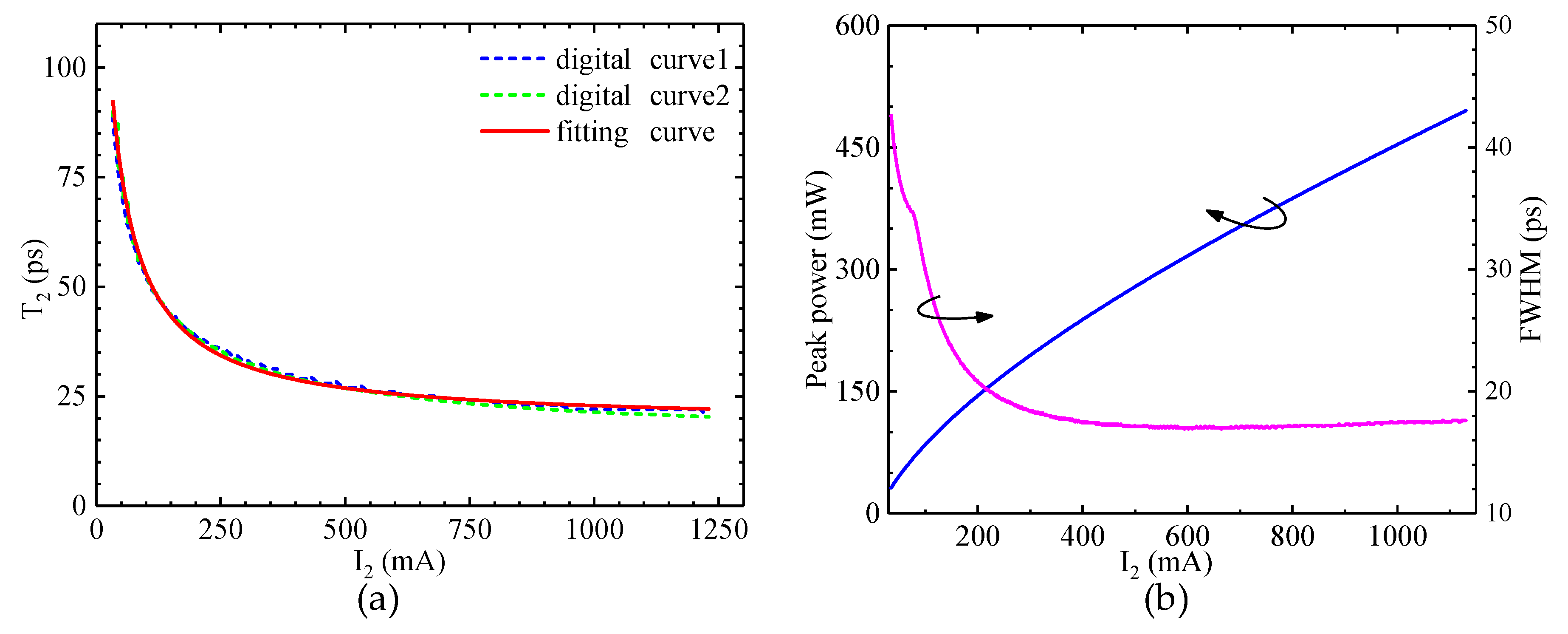
Figure 5a is the relation between
and
, in which the green curve2 is the result based on conclusion one, and the blue curve1 is the result based on conclusion two. It can be seen clearly that curves1 and 2 are basically coincident. To fit the curve1 and curve2 separately, we design an inverse function expression as follows:
where the units of
and
are mA and ps. In the experimental data disposal, the coefficient of determination is often used as a criterion of fitting goodness. In the case of
mA and
ns, calculations showed that the coefficient of determination of the fitting curve to curve1 is 0.99139, and the coefficient of determination for curve2 is 0.99242, when
mA∙ps,
mA,
ps. Therefore, Equation (4) can be used to characterize the relationship between
and
.
Figure 5b shows the variation of the peak power and the FWHM of the output pulse when
and
satisfy the relationship of Equation (4). According to the fitting curve in
Figure 5a, it is directly seen that: To get a short pulse with high peak power, firstly, we can increase
, and then reduce
, so that the output pulse is more and sharper at the same peak power, until
and
satisfy the analogous expression of Equation (4); when
increases indefinitely,
changes slowly and tends to be stable. At this time, although the peak power is still increasing, the output pulse width changes very little and tends to stabilize too.
4. Conclusions
The output characteristics of the gain-switched semiconductor laser are affected by the modulation signal and the intrinsic parameters of the laser. However, it is impossible to improve the performance of the output pulse by controlling the internal factors under the condition that the laser has been fabricated. According to the fact that the accumulation speed mainly determines the peak power and width of the output pulse after the carrier density reaches the threshold, we describe a method for generating ultra-short pulses with high extinction ratio based on step rectangular wave modulation. Then, through numerical simulation, the influence of amplitude and width of the second modulation current on the output pulse is discussed. It is concluded that when is constant, should be adjusted until the maximum time of output pulse power is equal to the injection current termination time. The moment is precisely the same as the injection current termination time; when is fixed, should be adjusted so that the output peak power just reaches saturation. At last, when the laser output pulse is optimal, the inverse proportional relationship between and is obtained by curve fitting. Compared with the rectangular wave modulation, it is shown that the step-pulse can increase the output pulse peak power by increasing the second modulation current and reduce the pulse width to saturation at the best working point. It should be noted that we did not consider the effect of temperature during modulation because of the mature of temperature control, which the precision could reach 0.01 degrees centigrade.
Although our simulation is based on the parameters in
Table 1, the results are applicable to other semiconductors with different parameters because the gain-switched process is always the same. The gain-switched pulse lasers with rectangular wave modulation have been studied for a long time and can be found in commercial products. Our method is an improvement to them, and it is not difficult to be achieved. In the real experiment, we can use the differential circuit in the falling edge of a square wave to generate spike as a scheme of generating step-pulse. Our method has excellent guidance for further improving the performance of the gain-switched semiconductor lasers and solving the application requirements for a high extinction ratio of short pulse signals, such as the optical time domain reflectometry.


