A Thiazolothiazole-Based Semiconducting Polymer with Well-Balanced Hole and Electron Mobilities


Abstract
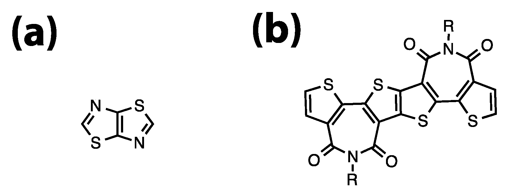
:1. Introduction
2. Methods and Materials
2.1. Materials
2.2. Instrumentation
2.3. Fabrication of OFET Devices and Measurement of the Transport Properties
2.4. Grazing Incident X-Ray Diffraction Measurements
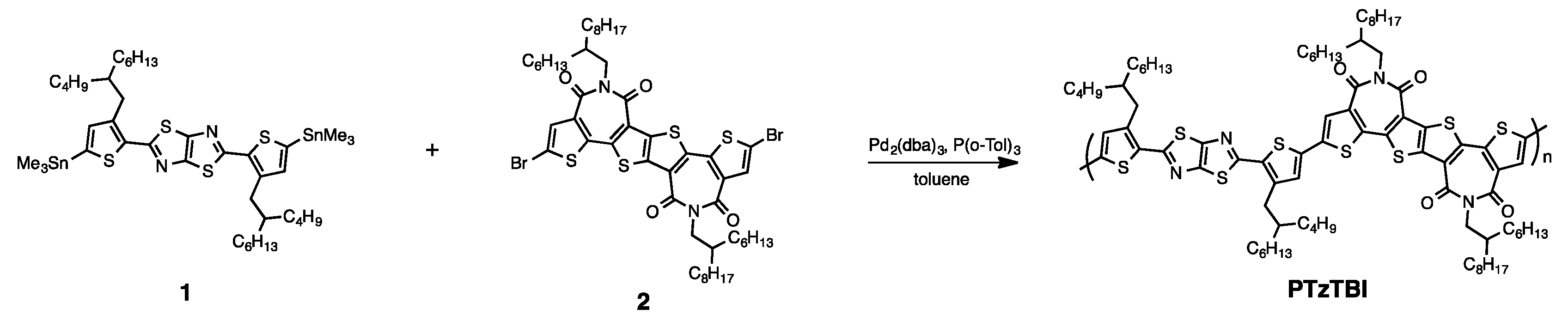
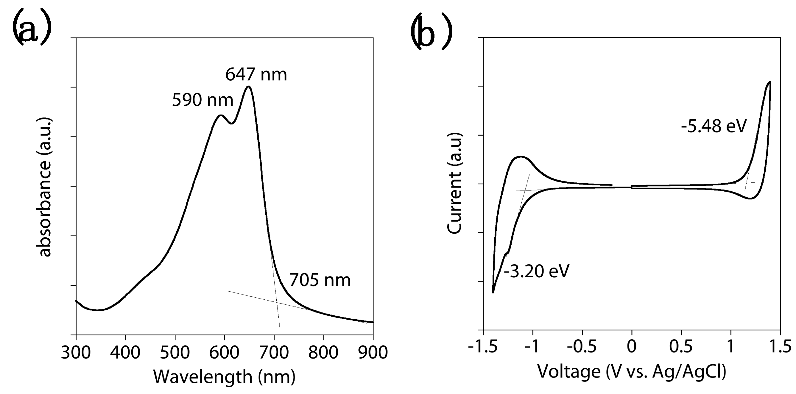
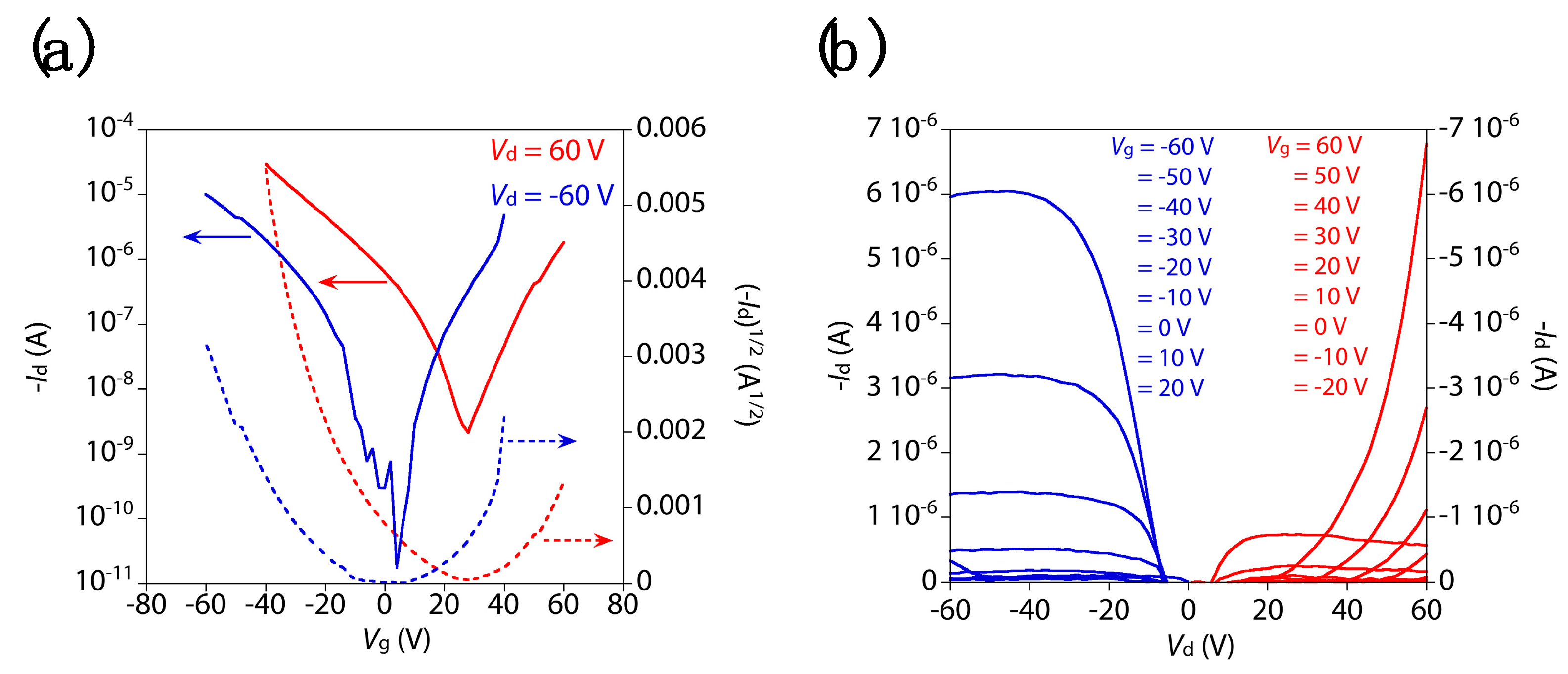
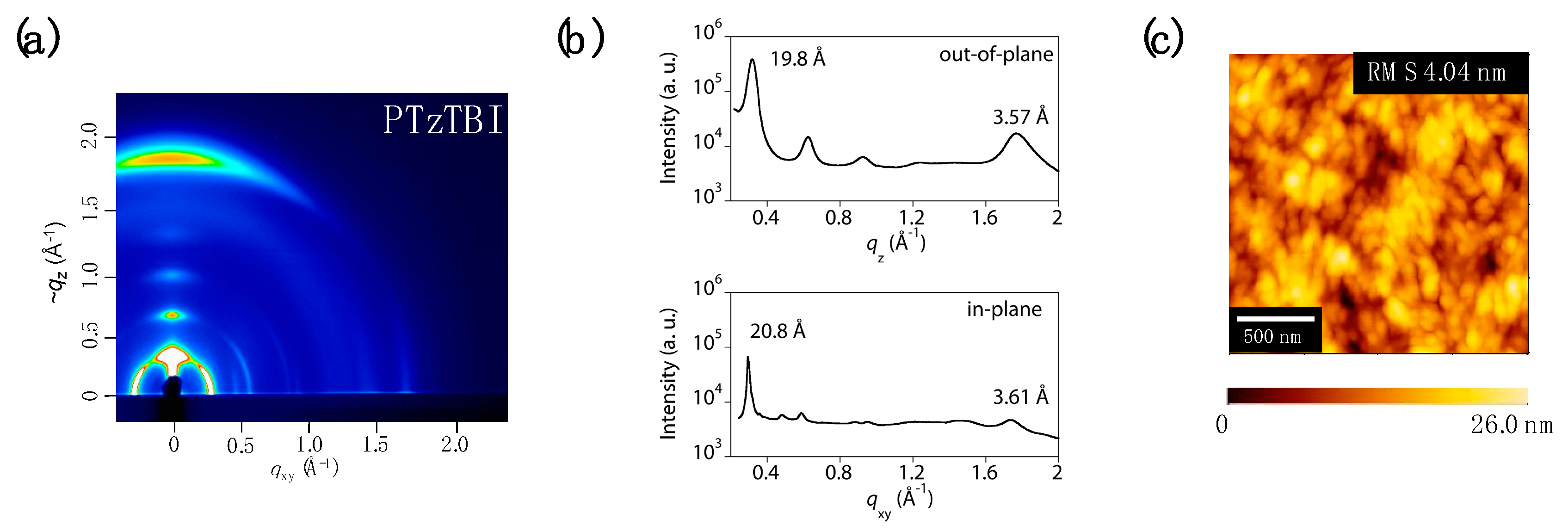
3. Results
4. Conclusions
Supplementary Materials
Author Contributions
Funding
Acknowledgments
Conflicts of Interest
References
- Sirringhaus, H. 25th Anniversary Article: Organic Field-Effect Transistors: The Path Beyond Amorphous Silicon. Adv. Mater. 2014, 26, 1319–1335. [Google Scholar] [CrossRef] [PubMed]
- McCulloch, I.; Heeney, M.; Chabinyc, M.L.; DeLongchamp, D.; Kline, R.J.; Colle, M.; Duffy, W.; Fischer, D.; Gundlach, D.; Hamadani, B.; et al. Semiconducting Thienothiophene Copolymers: Design, Synthesis, Morphology, and Performance in Thin-Film Organic Transistors. Adv. Mater. 2009, 21, 1091–1109. [Google Scholar] [CrossRef]
- Yu, G.; Gao, J.; Hummelen, J.C.; Wudl, F.; Heeger, A.J. Polymer Photovoltaic Cells: Enhanced Efficiencies via a Network of Internal Donor-acceptor Heterojunctions. Science 1995, 270, 1789–1791. [Google Scholar] [CrossRef]
- Günes, S.; Neugebauer, H.; Sariciftci, N.S. Conjugated Polymer-based Organic Solar Cells. Chem. Rev. 2007, 107, 1324–1338. [Google Scholar] [CrossRef] [PubMed]
- Grimsdale, A.C.; Chan, K.L.; Matrin, R.E.; Jokisz, P.G.; Holmes, A.B. Synthesis of Light-Emitting Conjugated Polymers for Applications in Electroluminescent Devices. Chem. Rev. 2009, 109, 897–1091. [Google Scholar] [CrossRef] [PubMed]
- Bao, Z.; Locklin, J. Organic Field-Effect Transistors; CRC Press: Boca Raton, FL, USA, 2007. [Google Scholar]
- Klauk, H. Organic Electronics II: More Materials and Applications; Wiley-VCH: Weinheim, Germany, 2012. [Google Scholar]
- McCulloch, I.; Heeney, M.; Bailey, C.; Genevicius, K.; MacDonald, I.; Shkunov, M.; Sparrowe, D.; Tierney, S.; Wagner, R.; Zhang, W.; et al. Liquid-crystalline semiconducting polymers with high charge-carrier mobility. Nat. Mater. 2006, 5, 328–333. [Google Scholar] [CrossRef]
- Osaka, I.; Abe, T.; Shinamura, S.; Takimiya, K. Impact of Isomeric Structures on Transistor Performances in Naphthodithiophene Semiconducting Polymers. J. Am. Chem. Soc. 2011, 133, 6852–6860. [Google Scholar] [CrossRef]
- Wang, S.; Kappl, M.; Liebewirth, I.; Muller, M.; Kirchhoff, K.; Pisula, W.; Mullen, K. Organic Field-Effect Transistors based on Highly Ordered Single Polymer Fibers. Adv. Mater. 2012, 24, 417–420. [Google Scholar] [CrossRef]
- Osaka, I.; Sauvé, G.; Zhang, R.; Kowalewski, T.; McCullough, R.D. Novel thiophene-thiazolothiazole copolymers for organic field-effect transistors. Adv. Mater. 2007, 19, 4160–4165. [Google Scholar] [CrossRef]
- Osaka, I.; Zhang, R.; Sauvé, G.; Smilgies, D.-M.; Kowalewski, T.; McCullough, R.D. Highly-lamellar ordering and amorphous-like π-network in short-chain thiazolothiazole-thiophenecopolymers lead to high mobilities. J. Am. Chem. Soc. 2009, 131, 2521–2529. [Google Scholar] [CrossRef]
- Osaka, I.; Zhang, R.; Liu, J.; Smilgies, D.-M.; Kowalewski, T.; McCullough, R.D. Highly stable semiconducting polymers based on thiazolothiazole. Chem. Mater. 2010, 22, 4191–4196. [Google Scholar] [CrossRef]
- Shi, Q.; Fan, H.; Liu, Y.; Hu, W.; Li, Y.; Zhan, X. A copolymer of benzodithiophene with TIPS side chain for enhanced photovoltaic performance. Macromolecules 2011, 44, 9173–9179. [Google Scholar] [CrossRef]
- Subramaniyan, S.; Xin, H.; Kim, F.S.; Jenekhe, S.A. New thiazolothiazole copolymer semiconductors for highly efficient solar cells. Macromolecules 2011, 44, 6245–6248. [Google Scholar] [CrossRef]
- Subramaniyan, S.; Xin, H.; Kim, F.S.; Shoae, S.; Durrant, J.R.; Jenekhe, S.A. Effect of side chains on thiazolothiazole-based copolymer semiconductors for high performance solar cell. Adv. Energy Mater. 2011, 1, 854–860. [Google Scholar] [CrossRef]
- Osaka, I.; Saito, M.; Mori, H.; Koganezawa, T.; Takimiya, K. Drastic change of molecular orientation in a thiazolothiazole copolymer by molecular-weight control and blending with PC61BM leads to high efficiencies in solar cells. Adv. Mater. 2012, 24, 425–430. [Google Scholar] [CrossRef] [PubMed]
- Subramaniyan, S.; Sunjoo, F.S.; Ren, G.; Li, H.; Jenekhe, S.A. High mobility thiazole-diketopyrrolopyrrole copolymer semiconductors for high performance field-effect transistors and photovoltaic devices. Macromolecules 2012, 45, 9029–9037. [Google Scholar] [CrossRef]
- Osaka, I.; Saito, M.; Koganezawa, T.; Takimiya, K. Thiophene-thiazolothiazole copolymers: Significant impact of side chain composition on backbone orientation and solar cell performances. Adv. Mater. 2014, 26, 331–338. [Google Scholar] [CrossRef]
- Ando, S.; Nishida, J.; Tada, H.; Inoue, Y.; Tokito, S.; Yamashita, Y. High Performance n-Type Organic Field-Effect Transistors Based on π-Electronic Systems with Trifluoromethylphenyl Groups. J. Am. Chem. Soc. 2005, 127, 5336–5337. [Google Scholar] [CrossRef]
- Takimiya, K.; Osaka, I.; Nakano, M. π-building blocks for organic electronics: Revaluation of ‘‘inductive’’ and “resonance” effect of π-electron deficient units. Chem. Mater. 2014, 26, 587–593. [Google Scholar] [CrossRef]
- Saito, M.; Osaka, I.; Suda, Y.; Yoshida, H.; Takimiya, K. Dithienylthienothiophenebisimide, a versatile electron-deficient unit for semiconducting polymers. Adv. Mater. 2016, 28, 6921–6925. [Google Scholar] [CrossRef]
- Rogers, J.T.; Schmidt, K.; Toney, M.F.; Kramer, E.J.; Bazan, G.C. Structural order in bulk heterojunction films prepared with solvent additives. Adv. Mater. 2011, 23, 2284–2288. [Google Scholar] [CrossRef] [PubMed]
- Roe, R.J. Methods of X-ray and Neutron Scattering in Polymer Science; Oxford University Press: New York, NY, USA, 2000. [Google Scholar]
- Saito, M.; Koganezawa, T.; Osaka, I. submitted.
- Duong, D.T.; Toney, M.F.; Salleo, A. Role of confinement and aggregation in charge transport in semicrystalline polythiophene thin films. Phys. Rev. B 2012, 86, 205205. [Google Scholar] [CrossRef]

© 2019 by the authors. Licensee MDPI, Basel, Switzerland. This article is an open access article distributed under the terms and conditions of the Creative Commons Attribution (CC BY) license (http://creativecommons.org/licenses/by/4.0/).
Share and Cite
Saito, M.; Osaka, I. A Thiazolothiazole-Based Semiconducting Polymer with Well-Balanced Hole and Electron Mobilities. Appl. Sci. 2019, 9, 451. https://doi.org/10.3390/app9030451
Saito M, Osaka I. A Thiazolothiazole-Based Semiconducting Polymer with Well-Balanced Hole and Electron Mobilities. Applied Sciences. 2019; 9(3):451. https://doi.org/10.3390/app9030451
Chicago/Turabian StyleSaito, Masahiko, and Itaru Osaka. 2019. "A Thiazolothiazole-Based Semiconducting Polymer with Well-Balanced Hole and Electron Mobilities" Applied Sciences 9, no. 3: 451. https://doi.org/10.3390/app9030451
APA StyleSaito, M., & Osaka, I. (2019). A Thiazolothiazole-Based Semiconducting Polymer with Well-Balanced Hole and Electron Mobilities. Applied Sciences, 9(3), 451. https://doi.org/10.3390/app9030451