High-Power GaN-Based Vertical-Cavity Surface-Emitting Lasers with AlInN/GaN Distributed Bragg Reflectors


Abstract
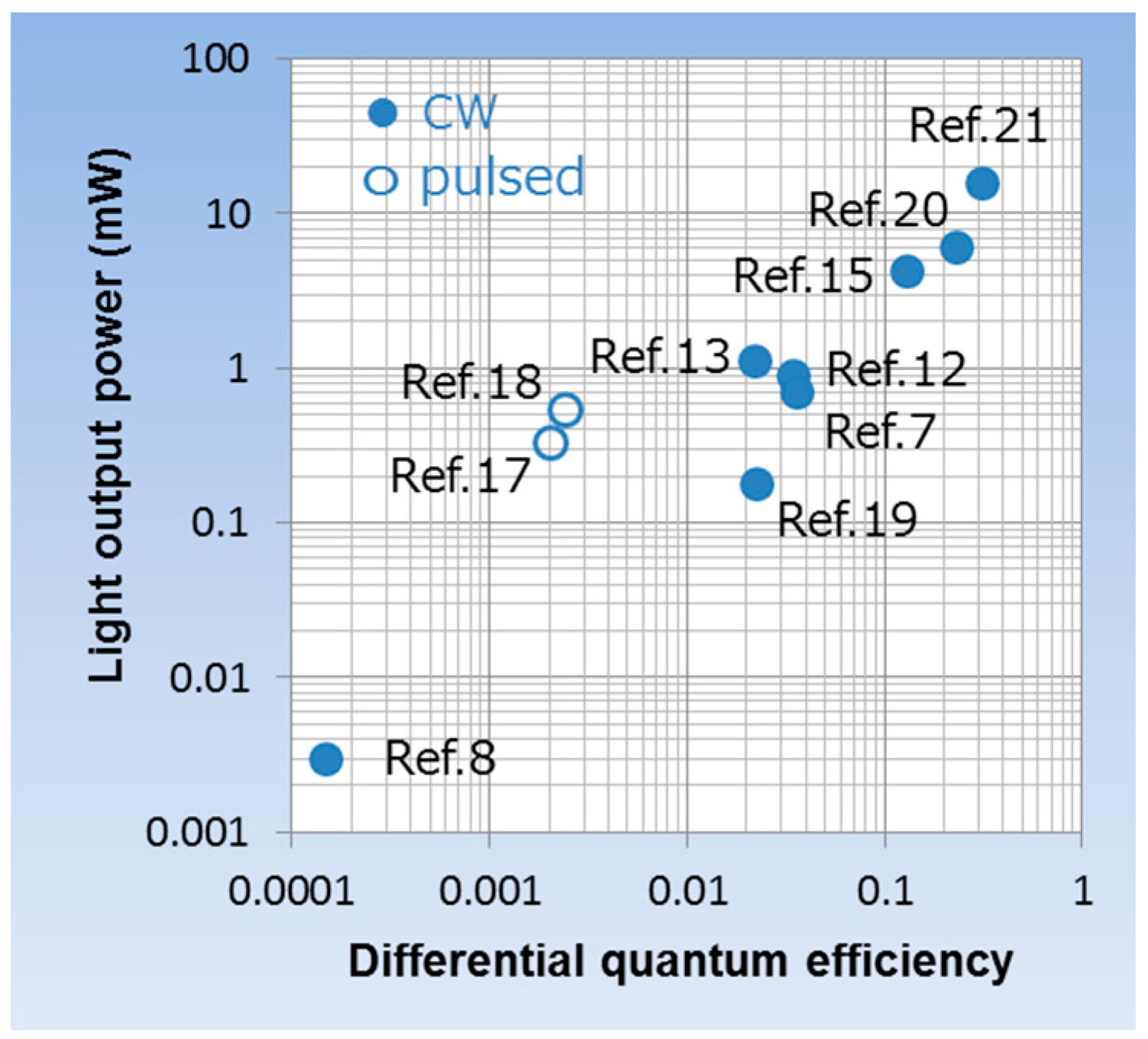
1. Introduction
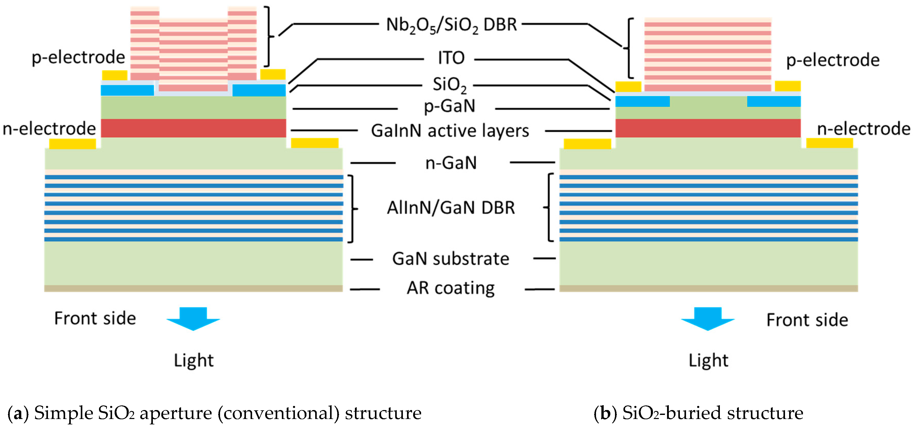
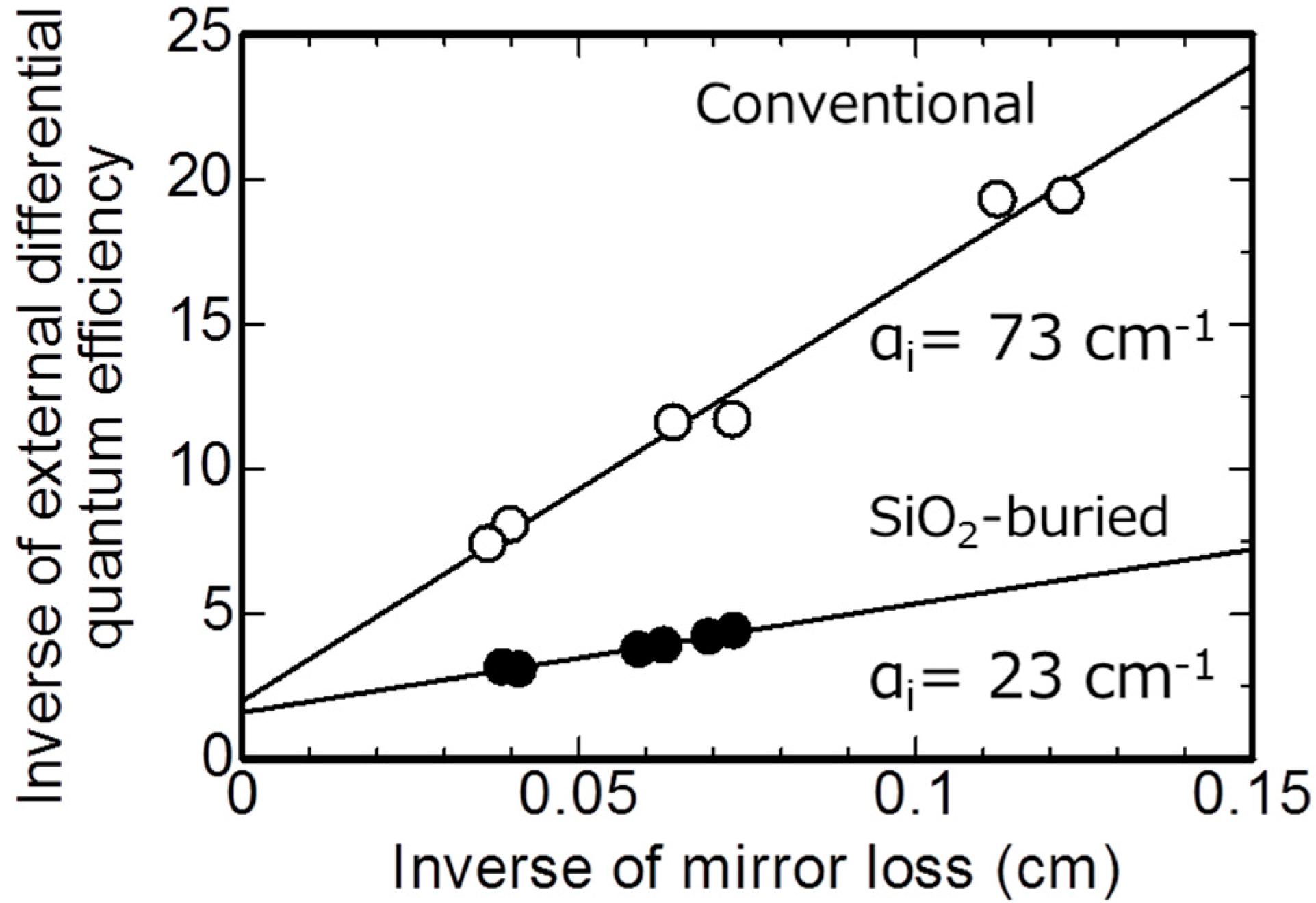
2. Enhancement of Differential Quantum Efficiency
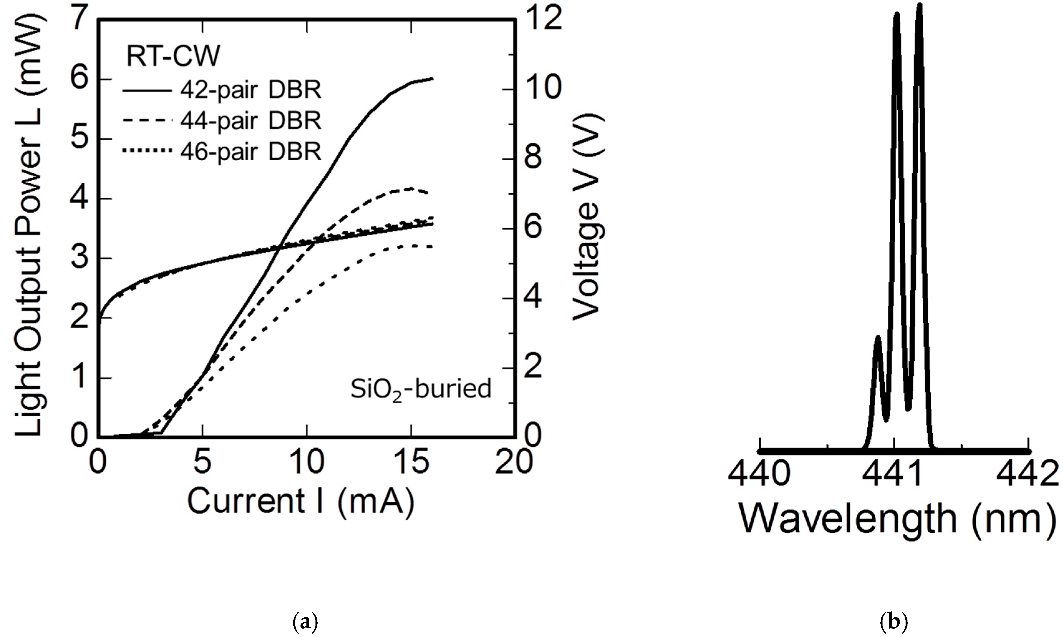
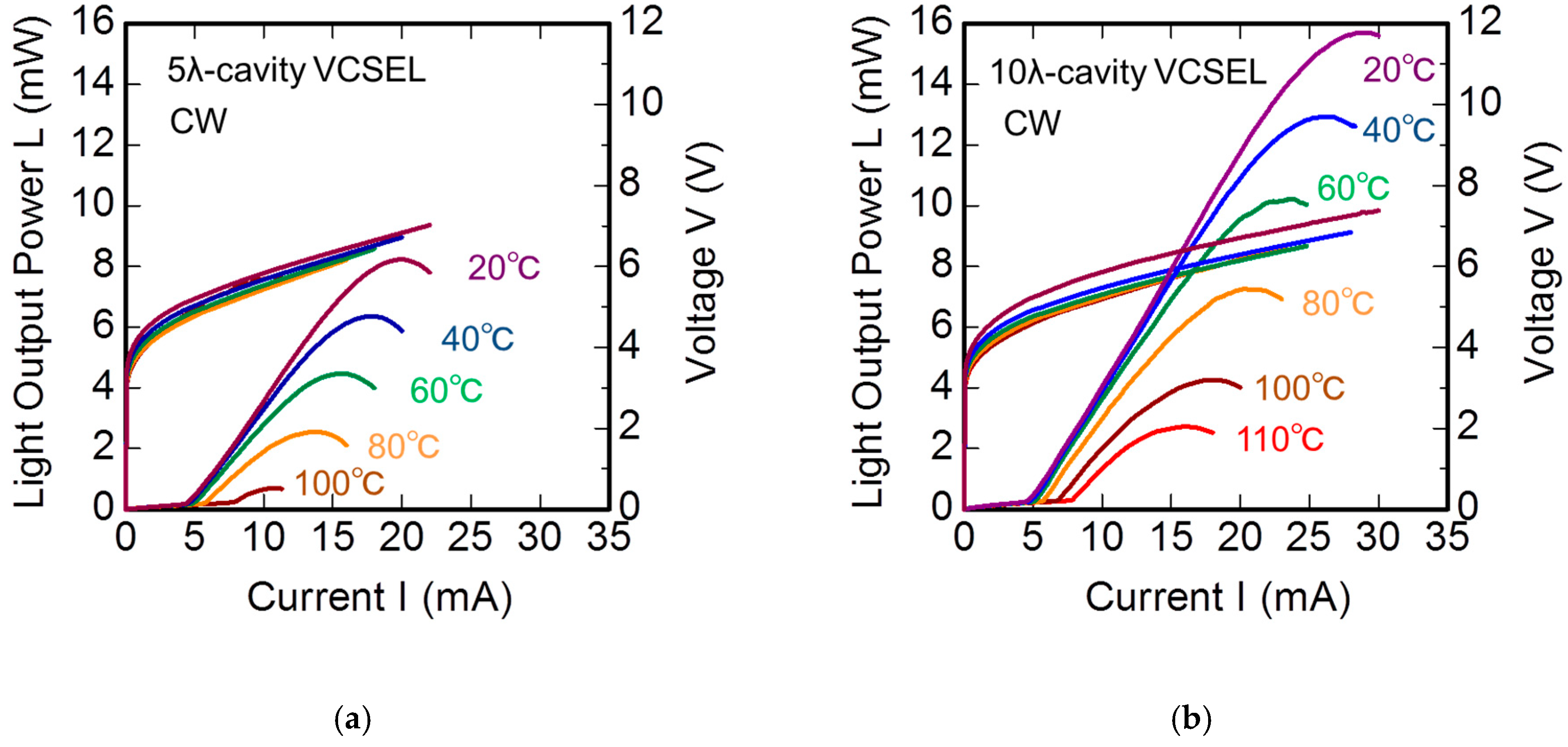
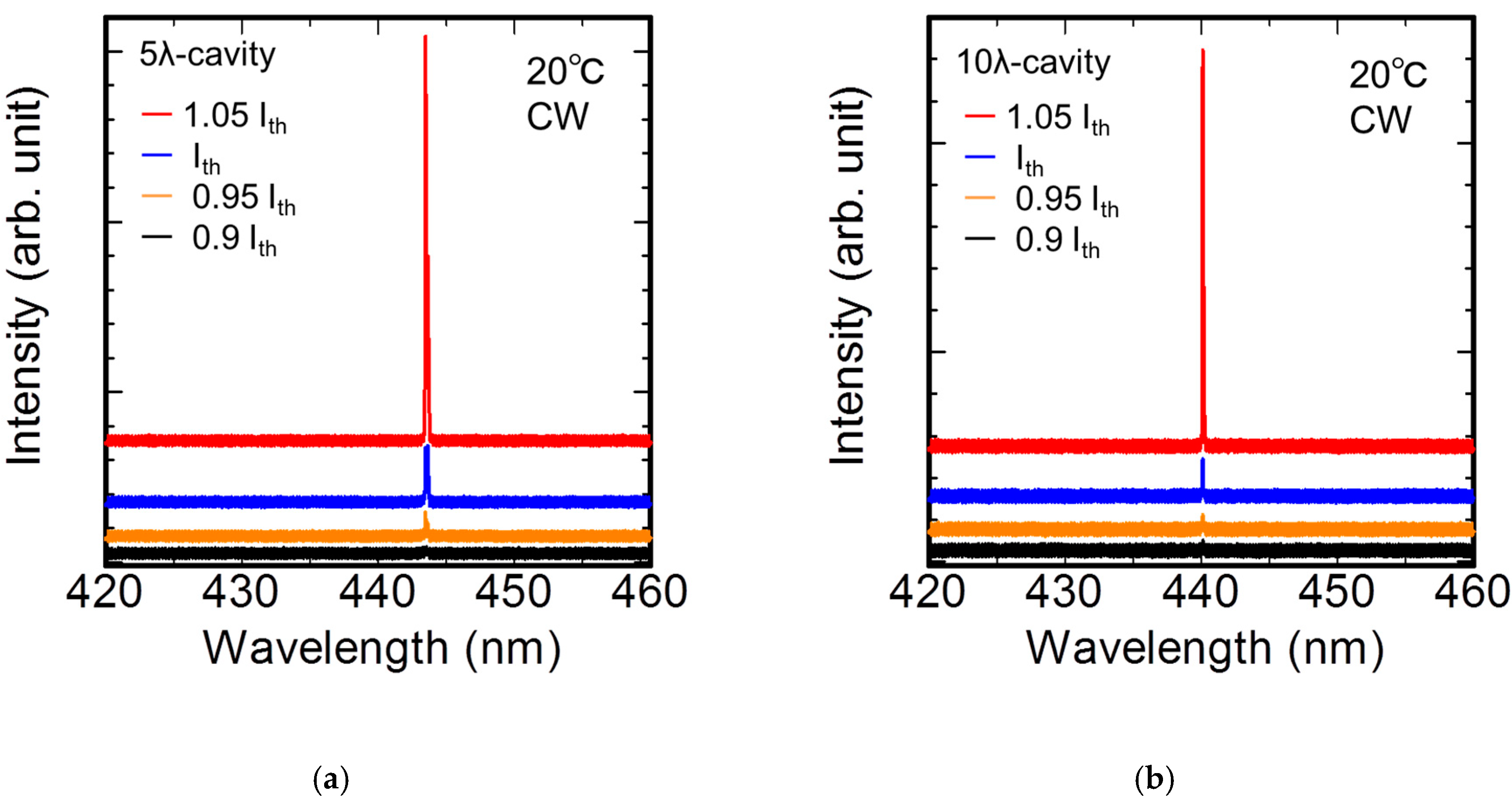
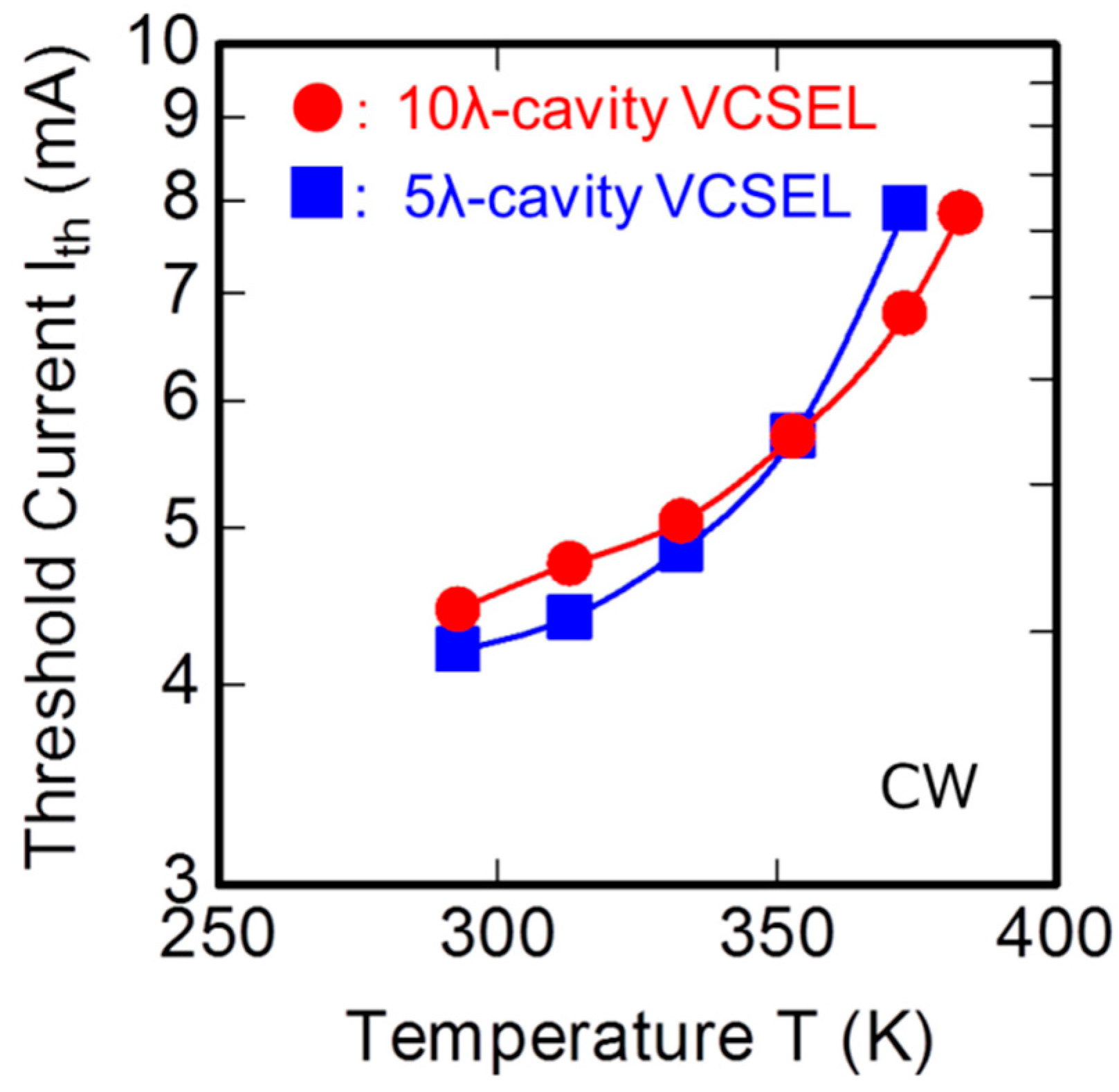
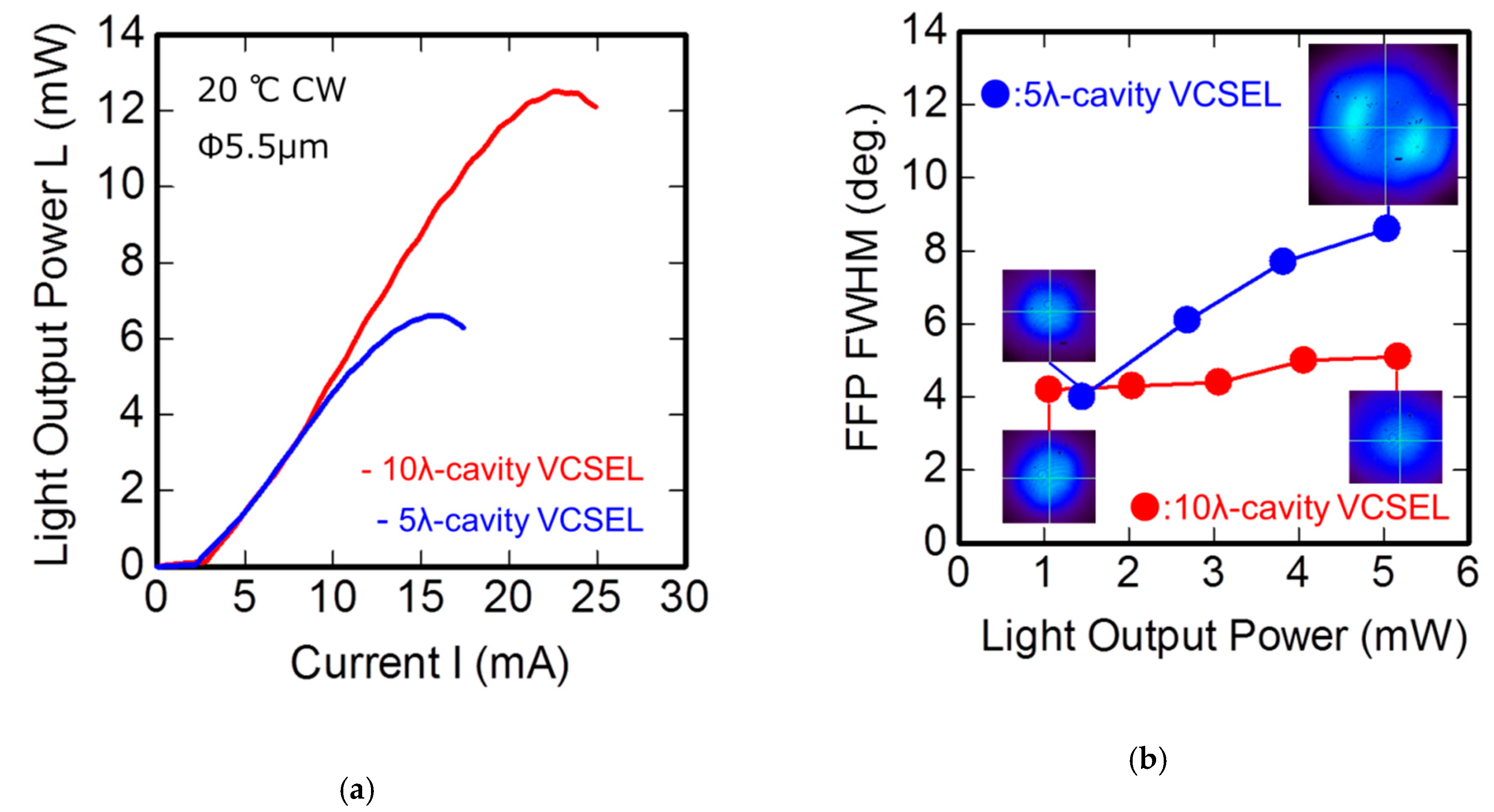
3. High-Power and Narrow Divergent Beam Performance Using a Long Cavity Structure
4. Conclusions
Author Contributions
Funding
Acknowledgments
Conflicts of Interest
References
- Hoshino, S.; Kita, Y.; Uchida, M.; Mori, T.; Kimura, Y.; Harata, S.; Saito, T.; Yatsuda, Y. Challenges for the laser scanning headlamps to realize safe driving experience. In Proceedings of the 12th International Symposium on Automotive Lighting; München Herbert Utz Verlag GmbH: München, Germany, 2017; Volume 17, pp. 299–305. [Google Scholar]
- Hager, J.; Seitz, M.; Bemmer, C.; Jahn, P.; Ansorg, P.; Woisetschlager, O.; Buchmann, F.; Sprenger, D.; Vogl, M.; Hering, O.; et al. Handling 17W of scanning laser power—Three years of exploration in the iLaS project. In Proceedings of the 12th International Symposium on Automotive Lighting; München Herbert Utz Verlag GmbH: München, Germany, 2017; Volume 17, pp. 271–280. [Google Scholar]
- Stroop, P.; Hilling, B.; Steudel, F.; Nolte, P. LASER scanning lighting systems—Optimization of contrast and further challenges. In Proceedings of the SIA VISION, Paris, France, 9–10 October 2018; Volume 2018, pp. 167–172. [Google Scholar]
- Lu, T.C.; Kao, C.C.; Kuo, H.C.; Huang, G.S.; Wang, S.C. CW lasing of current injection blue GaN-based vertical cavity surface emitting laser. Appl. Phys. Lett. 2008, 15, 141102. [Google Scholar] [CrossRef]
- Higuchi, Y.; Omae, K.; Matsumura, H.; Mukai, T. Room-Temperature CW Lasing of a GaN-Based Vertical-Cavity Surface-Emitting Laser by Current Injection. Appl. Phys. Express 2008, 1, 121102. [Google Scholar] [CrossRef]
- Lu, T.C.; Chen, S.W.; Wu, T.T.; Tu, P.M.; Chen, C.K.; Chen, C.H.; Li, Z.Y.; Kuo, H.C.; Wang, S.C. Continuous wave operation of current injected GaN vertical cavity surface emitting lasers at room temperature. Appl. Phys. Lett. 2010, 97, 071114. [Google Scholar] [CrossRef]
- Kasahara, D.; Morita, D.; Kosugi, T.; Nakagawa, K.; Kawamata, J.; Higuchi, Y.; Matsumura, H.; Mukai, T. Demonstration of Blue and Green GaN-Based Vertical-Cavity Surface-Emitting Lasers by Current Injection at Room Temperature. Appl. Phys. Express 2011, 4, 072103. [Google Scholar] [CrossRef]
- Onishi, T.; Imafuji, O.; Nagamatsu, K.; Kawaguchi, M.; Yamanaka, K.; Takigawa, S. Continuous Wave Operation of GaN Vertical Cavity Surface Emitting Lasers at Room Temperature. IEEE J. Quantum Electron. 2012, 48, 1107–1112. [Google Scholar] [CrossRef]
- Liu, W.-J.; Hu, X.-L.; Ying, L.Y.; Zhang, J.-Y.; Zhang, B.-P. Room temperature continuous wave lasing of electrically injected GaN-based vertical cavity surface emitting lasers. Appl. Phys. Lett. 2014, 104, 251116. [Google Scholar] [CrossRef]
- Izumi, S.; Fuutagawa, N.; Hamaguchi, T.; Murayama, M.; Kuramoto, M.; Narui, H. Room-temperature continuous-wave operation of GaN-based vertical-cavity surface-emitting lasers fabricated using epitaxial lateral overgrowth. Appl. Phys. Express 2015, 8, 062702. [Google Scholar] [CrossRef]
- Furuta, T.; Matsui, K.; Horikawa, K.; Ikeyama, K.; Kozuka, Y.; Yoshida, S.; Akagi, T.; Takeuchi, T.; Kamiyama, S.; Iwaya, M.; et al. Room-temperature CW operation of a nitride-based vertical-cavity surface-emitting laser using thick GaInN quantum wells. Jpn. J. Appl. Phys. 2016, 55, 05FJ11. [Google Scholar] [CrossRef]
- Hsieh, D.H.; Tzou, A.J.; Kao, T.S.; Lai, F.I.; Lin, D.W.; Lin, B.C.; Lu, T.C.; Lai, W.C.; Chen, C.H.; Kuo, H.C. Improved carrier injection in GaN-based VCSEL via AlGaN/GaN multiple quantum barrier electron blocking layer. Opt. Express 2015, 23, 27145–27151. [Google Scholar] [CrossRef]
- Hamaguchi, T.; Fuutagawa, N.; Izumi, S.; Murayama, M.; Narui, H. Milliwatt-class GaN-based blue vertical-cavity surface-emitting lasers fabricated by epitaxial lateral overgrowth. Phys. Status Solidi A 2016, 213, 1–7. [Google Scholar] [CrossRef]
- Hayashi, N.; Ogimoto, J.; Matsui, K.; Furuta, T.; Akagi, T.; Iwayama, S.; Takeuchi, T.; Kamiyama, S.; Iwaya, M.; Akasaki, I. A GaN-Based VCSEL with a Convex Structure for Optical Guiding. Phys. Status Solidi 2018, 215, 1700648. [Google Scholar] [CrossRef]
- Takeuchi, T.; Kamiyama, S.; Iwaya, M.; Akasaki, I. GaInN VCSELs with AlInN/GaN DBRs. In Proceedings of the International Conference on Nitride Semiconductors, Strasbourg, France, 24–28 July 2017. [Google Scholar]
- Yu, H.C.; Zheng, Z.W.; Mei, Y.; Xu, R.B.; Liu, J.P.; Yang, H.; Zhang, B.P.; Lu, T.C.; Kuo, H.C. Progress and prospects of GaN-based VCSEL from near UV to green emission. Prog. Quantum Electron. 2018, 57, 1–19. [Google Scholar] [CrossRef]
- Cosendey, G.; Castiglia, A.; Rossbach, G.; Carin, J.F.; Grandjean, N. Blue monolithic AlInN-based vertical cavity surface emitting laser diode on free-standing GaN substrate. Appl. Phys. Lett. 2012, 101, 151113. [Google Scholar] [CrossRef]
- Leonard, J.T.; Young, E.C.; Yonkee, B.P.; Cohen, D.A.; Margalith, T.; Denbaars, S.P.; Speck, J.S.; Nakamura, S. Demonstration of a III-nitride vertical-cavity surface-emitting laser with a III-nitride tunnel junction intracavity contact. Appl. Phys. Lett. 2015, 107, 091105. [Google Scholar] [CrossRef]
- Xu, R.; Mei, Y.; Xu, H.; Ying, L.Y.; Zheng, Z.; Long, H.; Zhang, D.; Zhang, B.; Liu, J. Green Vertical-Cavity Surface-Emitting Lasers Based on Combination of Blue-Emitting Quantum Wells and Cavity-Enhanced Recombination. IEEE Trans. Electr. Devices 2018, 65, 4401–4406. [Google Scholar] [CrossRef]
- Kuramoto, M.; Kobayashi, S.; Akagi, T.; Tazawa, K.; Tanaka, K.; Saito, T.; Takeuchi, T. Enhancement of slope efficiency and output power in GaN-based vertical-cavity surface-emitting lasers with a SiO2-buried lateral index guide. Appl. Phys. Lett. 2018, 112, 111104. [Google Scholar] [CrossRef]
- Kuramoto, M.; Kobayashi, S.; Akagi, T.; Tazawa, K.; Tanaka, K.; Saito, T.; Takeuchi, T. High-output-power and high-temperature operation of blue GaN-based vertical-cavity surface-emitting laser. Appl. Phys. Express 2018, 11, 112101. [Google Scholar] [CrossRef]
- Ellafi, D.; Iakovlev, V.; Sirbu, A.; Grigore, S.; Mickovic, Z.; Caliman, A.; Mereuta, A.; Kapon, E. Effect of Cavity Lifetime Variation on the Static and Dynamic Properties of 1.3-μm Wafer-Fused VCSELs. IEEE J. Sel. Top. Quantum Electron. 2015, 21, 1700509. [Google Scholar] [CrossRef]
- Hashemi, E.; Bengtsson, J.; Gustavsson, J.; Stattin, M.; Cosendey, G.; Grandjean, N.; Haglund, A. Analysis of structurally sensitive loss in GaN-based VCSEL cavities and its effect on modal discrimination. Opt. Express 2014, 22, 411–426. [Google Scholar] [CrossRef]
- Hadley, G.R. Effective index model for vertical-cavity surface-emitting lasers. Opt. Lett. 1995, 20, 1483–1485. [Google Scholar] [CrossRef]
- Michalzik, R. VCSELs, Springer Series in Optical Science; Springer: Berlin, Germany, 2013; Volume 166, p. 38. [Google Scholar]
- Kuksenkov, D.V.; Temkin, H.; Swirthun, S. Measurement of internal quantum efficiency and losses in vertical cavity surface emitting lasers. Appl. Phys. Lett. 1995, 66, 1720–1722. [Google Scholar] [CrossRef]
- Westbergh, P.; Gustavsson, J.S.; Kogel, B.; Haglund, A.; Larsson, A. Impact of Photon Lifetime on High-Speed VCSEL Performance. IEEE J. Sel. Top. Quantum Electron. 2011, 17, 1603–1613. [Google Scholar] [CrossRef]
- Koyama, F.; Suematsu, Y.; Arai, S.; Tawee, T. 1.5–1.6 µm GaInAsP/InP dynamic-single-mode (DSM) lasers with distributed Bragg reflector. IEEE J. Quantum Electron. 1983, QE-19, 1042–1051. [Google Scholar] [CrossRef]
- Tong, H.; Zhang, J.; Liu, G.; Herbsommer, J.A.; Huang, G.S.; Tansu, N. Thermoelectric properties of lattice-matched AlInN alloy grown by metal organic chemical vapor deposition. Appl. Phys. Lett. 2010, 97, 112105. [Google Scholar] [CrossRef]
- Zhang, J.; Tong, H.; Liu, G.; Herbsommer, J.A.; Huang, G.S.; Tansu, N. Characterizations of Seebeck coefficients and thermoelectric figures of merit for AlInN alloys with various In-contents. J. Appl. Phys. 2011, 109, 053706. [Google Scholar] [CrossRef]
- Zou, J.; Kotchetkov, D.; Balandin, A.A.; Florescu, D.I.; Pollak, H. Thermal conductivity of GaN films: Effects of impurities and dislocations. J. Appl. Phys. 2002, 92, 2534–2539. [Google Scholar] [CrossRef]
- Shibata, H.; Waseda, Y.; Ohta, H.; Kiyomi, K.; Shimoyama, K.; Fujito, K.; Nagaoka, H.; Kagamitani, Y.; Simura, R.; Fukuda, T. High Thermal Conductivity of Gallium Nitride (GaN) Crystals Grown by HVPE Process. Mater. Trans. 2007, 48, 2782–2786. [Google Scholar] [CrossRef]
- Mishkat-UI-Masabih, S.; Leonard, J.; Cohen, D.; Nakamura, S.; Feezell, D. Techniques to reduce thermal resistance in flip-chip GaN-based VCSELs. Phys. Status Solidi A 2017, 214, 1600819. [Google Scholar] [CrossRef]
- Chang, T.-C.; Kuo, S.-Y.; Lian, J.-T.; Hong, K.-B.; Wang, S.-C.; Lu, T.-C. High-temperature operation of GaN-based vertical-cavity surface-emitting lasers. Appl. Phys. Express 2017, 10, 112101. [Google Scholar] [CrossRef]
- Mei, Y.; Xu, R.-B.; Xu, H.; Ying, L.-Y.; Zheng, Z.-W.; Zhang, B.-P.; Li, M.; Zhang, J. A comparative study of thermal characteristics of GaN-based VCSELs with three different typical structures. Semicond. Sci. Technol. 2018, 33, 015016. [Google Scholar] [CrossRef]
- Michalzik, R. VCSELs, Springer Series in Optical Science; Springer: Berlin, Germany, 2013; Volume 166, p. 19. [Google Scholar]
- Lu, T.-C.; Wu, T.-T.; Chen, S.-W.; Tu, P.-M.; Li, Z.-Y.; Chen, C.-K.; Chen, C.-H.; Kuo, H.-C.; Wang, S.-C.; Zan, H.-W.; et al. Characteristics of Current-Injected GaN-Based Vertical-Cavity Surface-Emitting Lasers. IEEE J. Sel. Top. Quantum Electron. 2011, 17, 1594–1601. [Google Scholar]
- Holder, C.O.; Leonard, J.T.; Farrell, R.M.; Cohen, D.A.; Yonkee, B.; Speck, J.S.; Denbaars, S.P.; Nakamura, S.; Feezell, D.F. Nonpolar III-nitride vertical-cavity surface emitting lasers with a polarization ratio of 100% fabricated using photoelectrochemical etching. Appl. Phys. Lett. 2014, 105, 031111. [Google Scholar] [CrossRef]
- Lu, B.; Zhou, P.; Cheng, J.; Malloy, J.; Zolper, J.C. High temperature pulsed and continuous-wave operation and thermally stable threshold characteristics of vertical-cavity surface-emitting lasers grown by metalorganic chemical vapor deposition. Appl. Phys. Lett. 1994, 65, 1337–1339. [Google Scholar] [CrossRef]
- Yeh, P.S.; Chang, C.-C.; Chen, Y.-T.; Lin, D.-W.; Liou, J.-S.; Wu, C.C.; He, J.H.; Kuo, H.-C. GaN-based vertical-cavity surface emitting lasers with sub-milliamp threshold and small divergence angle. Appl. Phys. Lett. 2016, 109, 241103. [Google Scholar] [CrossRef]


© 2019 by the authors. Licensee MDPI, Basel, Switzerland. This article is an open access article distributed under the terms and conditions of the Creative Commons Attribution (CC BY) license (http://creativecommons.org/licenses/by/4.0/).
Share and Cite
Kuramoto, M.; Kobayashi, S.; Akagi, T.; Tazawa, K.; Tanaka, K.; Saito, T.; Takeuchi, T. High-Power GaN-Based Vertical-Cavity Surface-Emitting Lasers with AlInN/GaN Distributed Bragg Reflectors. Appl. Sci. 2019, 9, 416. https://doi.org/10.3390/app9030416
Kuramoto M, Kobayashi S, Akagi T, Tazawa K, Tanaka K, Saito T, Takeuchi T. High-Power GaN-Based Vertical-Cavity Surface-Emitting Lasers with AlInN/GaN Distributed Bragg Reflectors. Applied Sciences. 2019; 9(3):416. https://doi.org/10.3390/app9030416
Chicago/Turabian StyleKuramoto, Masaru, Seiichiro Kobayashi, Takanobu Akagi, Komei Tazawa, Kazufumi Tanaka, Tatsuma Saito, and Tetsuya Takeuchi. 2019. "High-Power GaN-Based Vertical-Cavity Surface-Emitting Lasers with AlInN/GaN Distributed Bragg Reflectors" Applied Sciences 9, no. 3: 416. https://doi.org/10.3390/app9030416
APA StyleKuramoto, M., Kobayashi, S., Akagi, T., Tazawa, K., Tanaka, K., Saito, T., & Takeuchi, T. (2019). High-Power GaN-Based Vertical-Cavity Surface-Emitting Lasers with AlInN/GaN Distributed Bragg Reflectors. Applied Sciences, 9(3), 416. https://doi.org/10.3390/app9030416