Article

A Visible and Near-IR Tunnel Photosensor with a Nanoscale Metal Emitter: The Effect of Matching of Hot Electrons Localization Zones and a Strong Electrostatic Field

1
Laboratory of System Problems in Control and Automation in Mechanical Engineering, Institute of Precision Mechanics and Control, RAS, 410028 Saratov, Russia
2
Volga-Svet Co. Ltd., 410052 Saratov, Russia
3
Department of Optics and Biophotonics, Faculty of Physics, Saratov State University, 410012 Saratov, Russia
4
Laboratory of Laser Diagnostics of Technical and Living Systems, Institute of Precision Mechanics and Control, RAS, 410028 Saratov, Russia
5
Department of Physics, Yury Gagarin State Technical University of Saratov, 410054 Saratov, Russia
*
Author to whom correspondence should be addressed.
Appl. Sci. 2019, 9(24), 5356; https://doi.org/10.3390/app9245356
Submission received: 10 October 2019 / Revised: 23 November 2019 / Accepted: 3 December 2019 / Published: 8 December 2019
(This article belongs to the Special Issue Nano-Photonics Materials and Devices)

Abstract

:
The results of the research and design of a novel vacuum photosensor with a planar molybdenum blade structure are presented. The advanced prototype implements the principle of an increasing penetrability of the Schottky barrier for the metal–vacuum interfaces under the action of an external strong electrostatic field. Theoretical and experimental substantiation of the photosensor performance in a wide range of wavelengths (from 430 to 680 nm and from 800 to 1064 nm) beyond the threshold of the classical photoelectric effect is given. The finite element method was applied to calculate distribution of the optical and electrostatic fields inside the photosensor structure. The sensor current-to-light response was studied using the periodic pulsed irradiation with the tunable wavelength. It was shown that the nanoscale localization zones of two types are formed near the surface of the blade tip: the zone of an increased concentration of hot electrons localized inside the molybdenum blade, and the zone with an increased strength of the external electrostatic field localized outside the blade. In general, the mutual positions of these zones may not coincide, whereas the position of the first-type localization zone significantly varies with the changes in the wavelength of the irradiating light. This causes features in the spectrum of the quantum yield of the photosensor such as expressed non-monotonic behavior and occurrence of sharp dips. The design of the photosensor that provides matching of the positions for both types of localization zones was proposed; the manufactured prototypes of the designed device were experimentally studied. In the designed photosensor, the ballistic transport of photoelectrons in the vacuum gap with a strong field provides a possibility for the creation of ultra-fast optoelectronic devices, such as modulators, detectors, and generators.

1. Introduction

It is hard to overestimate the importance of high-performance photosensing devices and technologies for modern technical progress [1]. Typically, any photosensing device converts the incoming light to an electrical signal on the basis of photon absorption by a photosensitive material, with conversion of an optical into an electric signal realized. Important applications of such units as high-speed information transceivers and communication networks [2,3], various types of remote sensing using the photosensitive matrices [4], and ultrafast sources of hot electrons in vacuum microelectronics devices [5,6] should be mentioned.
In particular, significant research efforts in recent years have been focused on the creation of novel photosensing material platforms, allowing for control of the bandgap width as well as an increase in the efficiency of light absorption and generation of hot electrons [2,3,7]. For example, the structures based on ultrathin layers of semiconductors such as transition metal dichalcogenides with a fundamental absorption in the near infrared (NIR) and visible regions possess very favorable properties for successful applications in photonics and optoelectronics [8]. The nanoscaled 2D layered structures based on the black phosphorus [9] opened up new possibilities for the bandgap control. This ensures the photosensing tuning within a broad wavelength range (from the visible to the infrared). It should be noted, however, that all the mentioned photosensors are based on the internal photoelectric effect.
Photosensors based on the external photoelectric effect are required in the various areas of modern vacuum optoelectronics (for example, for rapid modulation of intense electron beams). In particular, the photocurrent in the vacuum under IR irradiation can be obtained using the structures based on the combination of low-dimensional semiconductor structures and plasmonic materials [10]. However, despite a high level of optical absorption and enhancement of excitation of plasmonic oscillations in these structures, there are problems related to significant electrical capacitance of the structure and, respectively, persistence of the charge transfer [10,11]. These problems can adversely affect the performance of a photosensor.
Photosensors with metal sensing elements are somewhat prominent in this series of devices. They have an undeniable advantage of a high rate of excitation of the electrons in the conduction band (hereinafter referred to as “free electrons”) and their transport into the vacuum. However, owing to a relatively high work function, the photoeffect is observed only under a short-wavelength irradiation (in particular, in the ultraviolet region). Only using the surface plasmon resonance and/or deformation of the Schottky barrier at the metal–vacuum interface, the desired result can be achieved. In particular, this approach was successfully applied using nanosized gold plasmon structures [5,6]. The periodicity of the arrays of planar emitters [5] and bulk emitters [6,12] was reduced to 1 µm; this value corresponds to the marginal possibilities of modern technologies based on the e-beam lithography. The gaps between the emitters were equal to 200 nm in the case of the planar structure, and 150 nm in the case of the bulk emitters. However, the necessity to provide a high-precision topology for such structures with the developed working surface makes the production of such devices very expensive and time-consuming. In addition, their functional properties become very sensitive to deviations in the technological parameters.
On the contrary, the photosensor design discussed in this work is sufficiently less sensitive to the above mentioned technological problems. Its production is based on the standard planar technology [13,14] and includes the photolithography, liquid etching, and magnetron sputtering deposition. In addition, the developed vacuum technology provides high performance and reproducibility of the devices. Another advantage is the application of molybdenum as the material platform for the discussed device, which is widely used in electron–vacuum instrumentation. Our work also presents the results of the examination of the developed vacuum photosensor in the wavelength ranging from the visible to the near IR.

2. Materials and Methods

2.1. The Design and Production Technology of a Photosensor

Application the planar cycle technology, which is traditional in manufacturing of solid-state multilayer structures, provides certain advantages in manufacturing the emitter blade structure. In particular, providing a precise submicron gap between the flat emitter and gate electrodes allows for the occurrence of high amplification of the local electrostatic field in the vicinity of the blade tip under relatively low voltages between the gate and the emitter. The photosensor in the vacuum glass case is shown in Figure 1a; Figure 1b displays the top view of the blade array. Schematic of the composition of a single molybdenum blade-emitter (1), the molybdenum gate electrode (3), and a silica layer (2) between them, which is used in modeling of the light-sensor interaction, are shown in Figure 1c. The gap between the emitter and the gate (thickness of the insulating SiO2 layer) is equal to 700 nm. The gap between the emitter and the case wall is 200 µm. The gate layer thickness is 200 nm and the emitter thickness is 300 nm.
The stages of photosensor manufacturing include various technologies of deposition, etching, heating, and pumping. In particular, the magnetron sputtering deposition is used in the creation of the molybdenum gate layer; PECVD (Plasma Enhanced Chemical Vapor Deposition) at 5.28 MHz HF and 100 W power is applied to create the silica layer; the photosensor is pumped out using the turbo-molecular and Penning-type pumps for one hour at the temperature equal to 320 °C (the residual pressure in the sealed case is 10−6 Torr).

2.2. The Free Path Length of Hot Electrons in Molybdenum

When a conduction electron interacts with a photon, it transits to a non-equilibrium (hot) state. Its energy can be estimated as EF + ± kT, where EF is the Fermi energy, is the photon energy, k is the Boltzmann constant, and T is the temperature. Typically, the characteristic time τ of non-equilibrium electron relaxation in metals is between 1 fs and 10 fs. In particular, the relaxation time for molybdenum is equal to 6 fs [15].
With the known characteristic time, the mean free path of hot electrons can be estimated as Lτ = τ⋅υ [16]. Here, υ is the maximal electron velocity, which is defined as υ = {2(EF + )/m}1/2 (m is the mass of the electron). Rough estimations of υ for molybdenum give the value with the order of υ = 1.6 × 10⁶ m/s. Accordingly, the mean free path of hot electrons in molybdenum is approximately equal to 10 nm.
The parameter Lτ is directly related to the maximal depth of the subsurface layer characterized by the non-zero probability of hot electron tunneling into the vacuum in the case when the electron momentum is directed perpendicularly to the emitter surface. That is why the mean free path of hot electrons is a fundamental parameter controlling the quantum yield of the sensor with the tunneling photoemission.
The classical photoelectric effect in the metals is observed if the resulting energy EF + of the nonequilibrium photon-interacting electron that was initially located in the conduction band near the Fermi level is larger than the work function φ0 [17]. In this case, the probability for a hot electron to escape from the metal is equal to the unity. Correspondingly, a long-wavelength cutoff for photoemission is defined as
λr(nm) = 1240/φ0 (eV).
The features of the photoelectric effect, taking into account the effect of the temperature T and irradiation with the wavelength near the red border in the ultraviolet area at r + kTφ0, were considered in terms of the quantum mechanics in Fowler’s work [18].
For molybdenum, λr = 288 nm, that is, it belongs to the ultraviolet (UV) range. Therefore, to ensure photosensitivity of the molybdenum emitter during irradiation in the visible and NIR ranges is a nontrivial task. Its solution is connected with the use of special impact methods in order to deform the potential Schottky barrier on the emitter surface and create conditions for realization of the tunnel photoemission mode.

2.3. A Model for Calculating the Optical Field in the Structure During Laser Irradiation

To consider the features forming the localization zone of the optical field, a boundary value problem with the corresponding boundary conditions is formulated in the structure under study, and the Helmholtz equation is solved using the finite element method in the computational domain, shown in Figure 1c. The width of the sensor element is 750 μm (can be seen from the photograph in Figure 1b). Thus, a width of more than 45 exceeds the half-period of the structure (16.5 μm). This allows us to neglect the edge effects in the mathematical modeling of wave processes and use the two-dimensional formulation of the problem as an acceptable approximation. To solve the problem, the Comsol Multiphysics 5.1 software package (Wave Optics module) was used. Irradiation of the structure, shown in Figure 1c, was simulated using the plane monochromatic wave in the visible and the near IR ranges. We considered the case of the normal light incidence from above over the structure with the polarization vector of the electric field lying in the plane of the figure. On the left and right boundaries of the computational domain, the continuity conditions for the normal component of the electric field and equality to the zero of the tangential component are specified. For the considered case of polarization of the incident wave in the plane of the figure, these boundaries become the symmetry planes. The field scattered by the structure is absorbed by PML (Perfectly Matched Layer) at the upper boundary of the computational domain. As the depth of the skin layer for Mo is less than the thickness of the gate electrode, an impedance boundary condition is used at the lower boundary. To describe the dielectric function of molybdenum, we used the interpolation data provided by M. Querry et al. [19], and for Si02, we used the data presented by L. Gao et al. [20].

2.4. A Model for Calculation of the Electrostatic Field in the Structure

To consider the features shaping the localization zone of the electrostatic field in the structure under study, a boundary value problem with the corresponding boundary conditions is formulated, and the Laplace equation is solved using the finite element method in the computational domain, shown in Figure 1c. On the gate, the potential Ug is set over the grounded housing of the device equal to the zero potential. In the symmetry planes passing vertically through the middle of the emitter and the middle of the gate, adiabatic boundary conditions are specified. The conditions for potential continuity and the normal vector of the electrical induction are fulfilled for all the boundary conjugation surfaces of dissimilar materials.

3. Results and Discussion

3.1. The Radiation Diffraction on the Structure

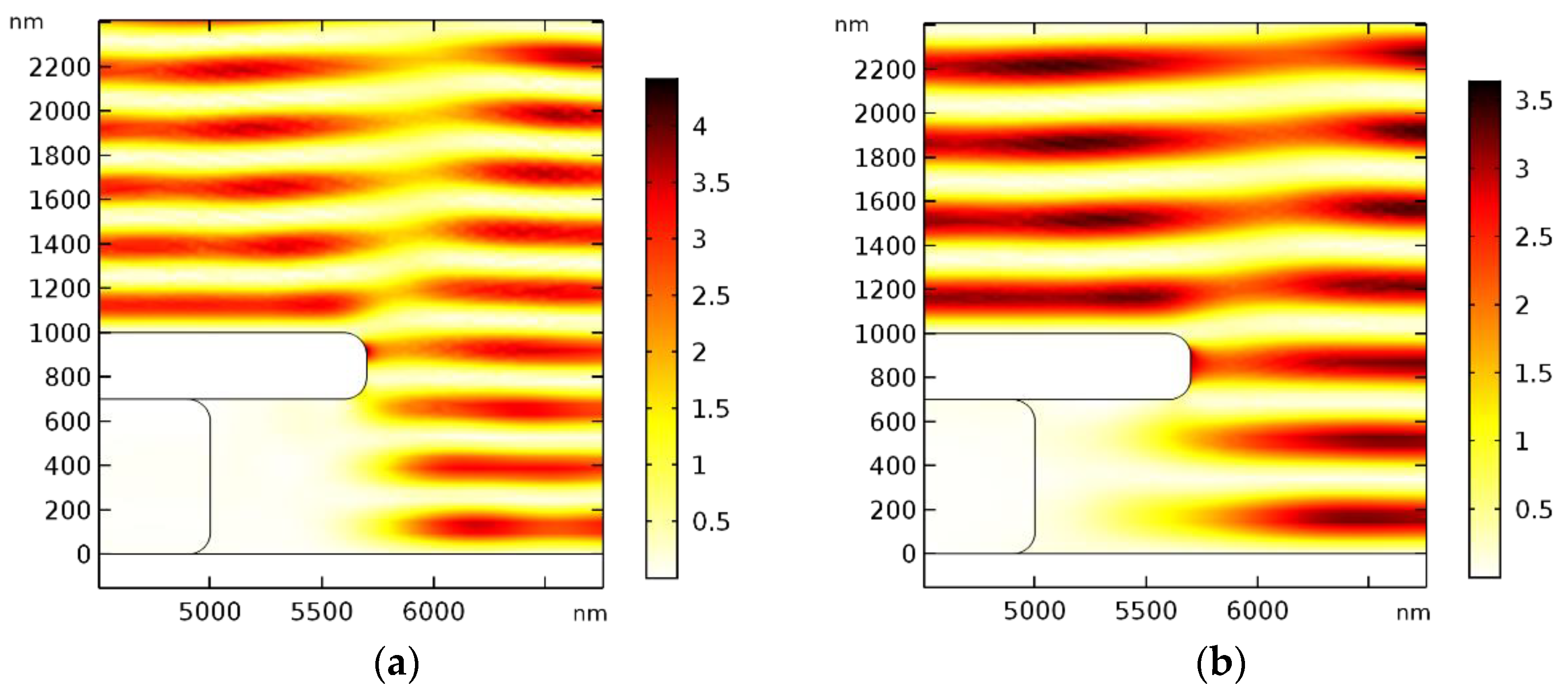
Figure 2 presents the calculation results of the irradiating light diffraction over the analyzed structure (AS). We consider a monochromatic plane electromagnetic wave, a normal incident on the AS in the negative direction of the y axis. This wave with the complex vector of the electric field E0 is linearly polarized along the x axis. Here are the normalized distributions of the squared absolute value of the electric vector |E|2/|E0|2, where E = Es + E0 is the complex vector of the total electric field, that is, the sum of the complex vectors of the scattered Es and the given irradiating E0 fields. These distributions, calculated at a wavelength of the illuminating beam of 500 nm and 700 nm, are presented in the fragments of Figure 2a,b, respectively.
It can be seen that the field distributions have the form of a series of bands with the minimum and maximum values alternating in the vertical direction with the period close to λ/2. These distributions have a pronounced interference structure characteristic of the standing waves with the alternating nodes and antinodes. Thus, the field distribution is largely determined by the interference of the waves, which are incident and reflected from the blade and the gate. With a change in λ, the location of the interference fringes changes. As a result, the tip of the blade may be in the region of low or high field values. This leads to migration of the areas of increased field absorption in the area of the tip of the blade-emitter, which is analyzed in the next section.

3.2. Spectral and Spatial Dependences of Amplification of the Optical and Electrostatic Fields on the Blade of the Structure

The efficiency of the photosensor is largely determined by the absorption intensity of radiation by its cathode. It is desirable to maximize this intensity and, consequently, the number of photoexcited (hot) electrons [21,22,23,24]. The local intensity value of radiation absorption is determined by the following equation [24]:
Q = 0.25·ν·ε|E|2,
where ν is the radiation frequency and ε is the imaginary part of the dielectric function of the absorbing material. The calculation of the local intensity distribution of radiation absorption is actually reduced to the calculation of the squared modulus distribution of the electric field vector |E|2 in the absorbing material. The results of the given calculation are presented in Figure 3.
The calculation results of the two-dimensional distribution of the function |E|2/|E0|2 inside the nanoscale tip of the molybdenum blade and outside in the vicinity of the tip, that is, in the vacuum, are presented in this figure. We can see a high degree of field localization in molybdenum in the near-surface layer, with the depth of several nanometers. In addition, there is a heterogeneity of the near-surface field in the orthogonal direction along the perimeter of the forming blade. Moreover, the location of these field inhomogeneities varies depending on the wavelength of the incident radiation. A similar pattern is observed near the tip of the emitter in the vacuum. The maxima of the field change their position along the perimeter of the forming blade with a change in the wavelength of the incident radiation. Thus, the spectral dependence of the areas of increased field absorption location in the emitter blade is obvious, which should be taken into account when choosing the operation modes of the given type of photosensors with increased efficiency.
The qualitative proximity of the field distribution in Figure 3a,c is explained by the fact that a node of a standing wave is located in the center of the end face of the blade. Field distribution in Figure 3b differs significantly from the previous ones owing to the fact that the antinode of the standing wave is located approximately in the center of the end face of the blade. We emphasize that near the nanosized edge of the blade, there is a significant deformation of the field distribution. As a result of this, in particular, the period of following nodes and antinodes decreases.
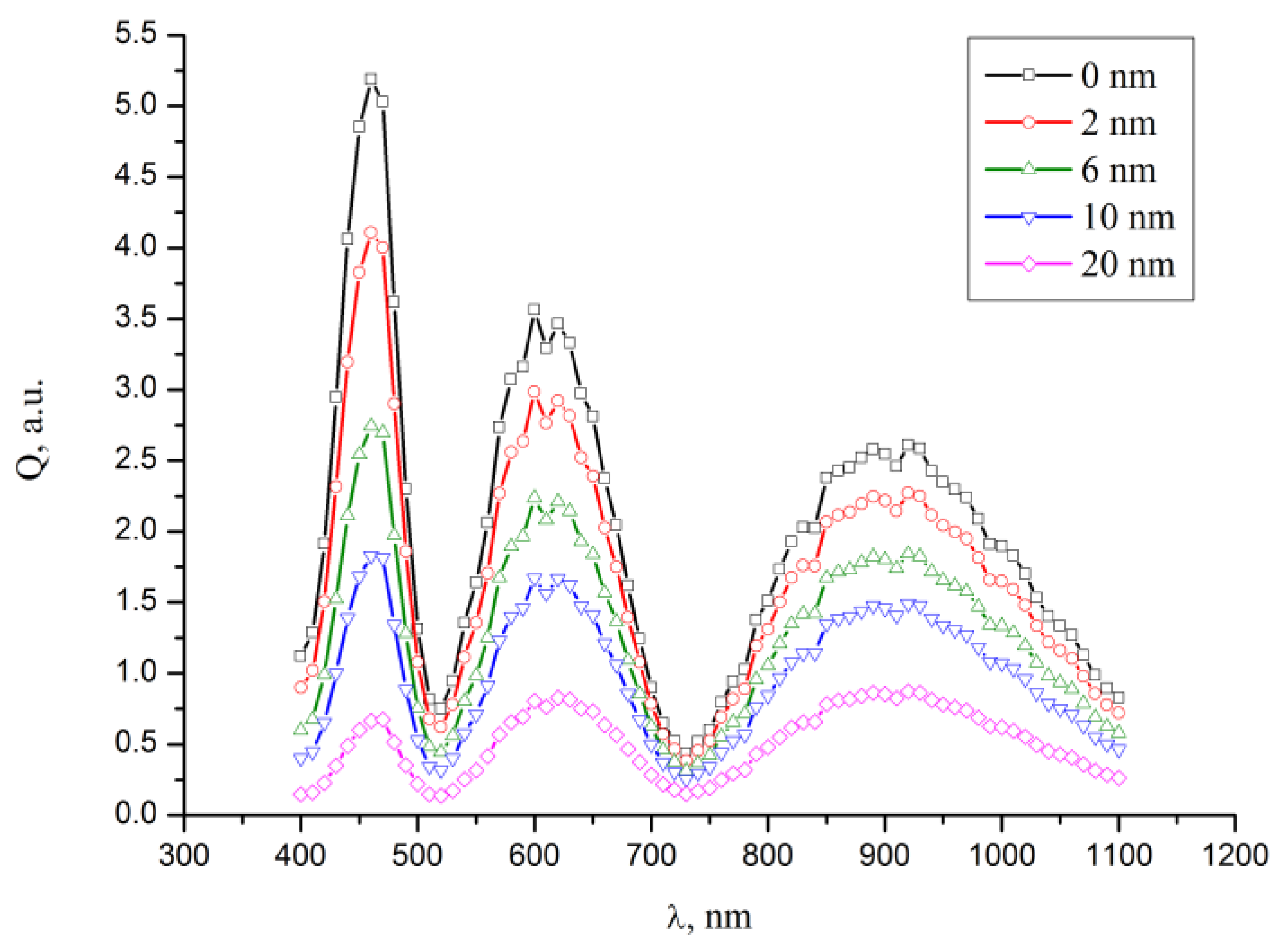
Formula (2) allows to quantify the specific power level of the absorbed photons and identify the patterns of their dependence on the absorption depth based on the analysis of results of spectral distribution estimation of the function presented in Figure 4. The calculation is carried out in the vicinity of point 2 (the designation is entered in Figure 3), which is located at the interface of the emitter tip rounding with its end surface. The curves in Figure 4 correspond to the specific absorption rate determined at different depths from the surface, starting from zero and ending at the depth of 20 nm. Additionally, we take into account that the data relating the specific absorbed power level are important in terms of estimating potential efficiency of the photosensor, as it is proportional to the concentration of hot electrons. Then, the top four curves in Figure 4 give a quantitative characteristic of the absorbed photon power, which is spent on excitation of the electrons, which can transport to the surface of the emitter (the depth is less than the free path of the hot electron in molybdenum Lτ = 10 nm).
An unexpected result referred not to the maxima or minima of the spectral absorption function, but to their significant difference in the magnitude (by 5–8 times depending on the wavelength of the radiation). The concentration of the hot electrons changes accordingly. It is also seen that the attenuation degree of the optical signal as the function of depth has spectral dependence. The observation point over the surface of the emitter tip was chosen arbitrarily during the computational experiment. However, an additional investigation demonstrated the existence of similar patterns in the other points across the emitter parameter.
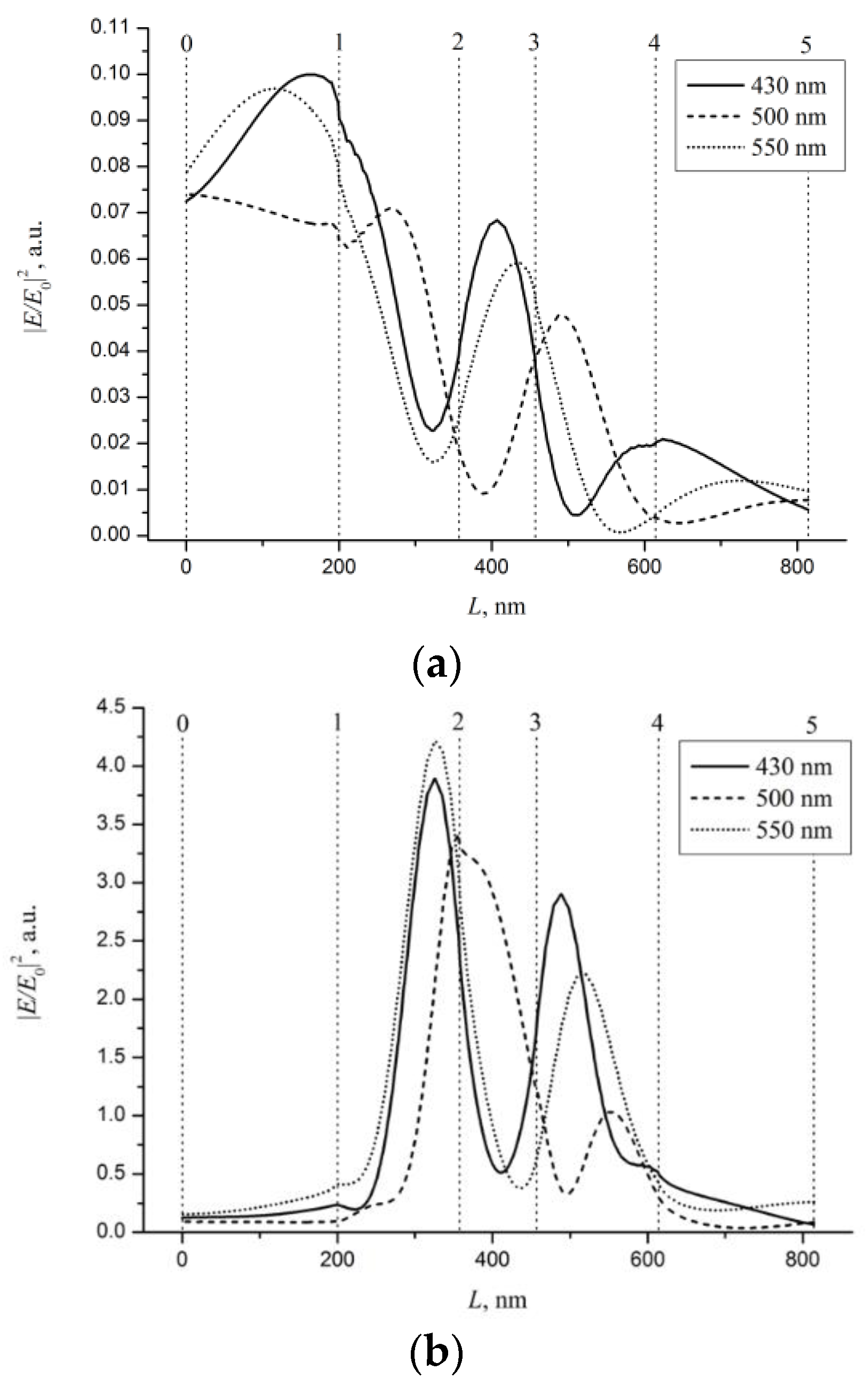
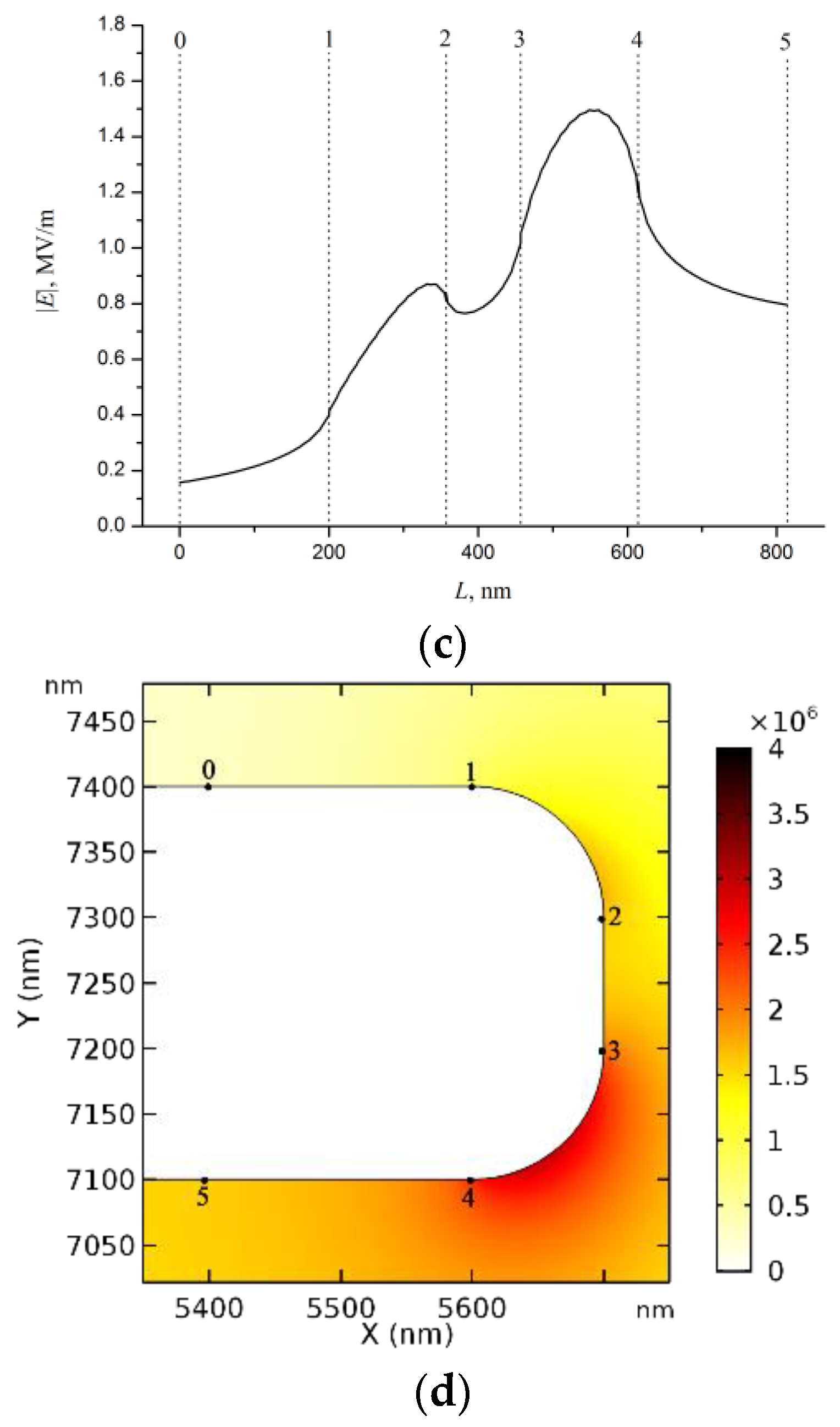
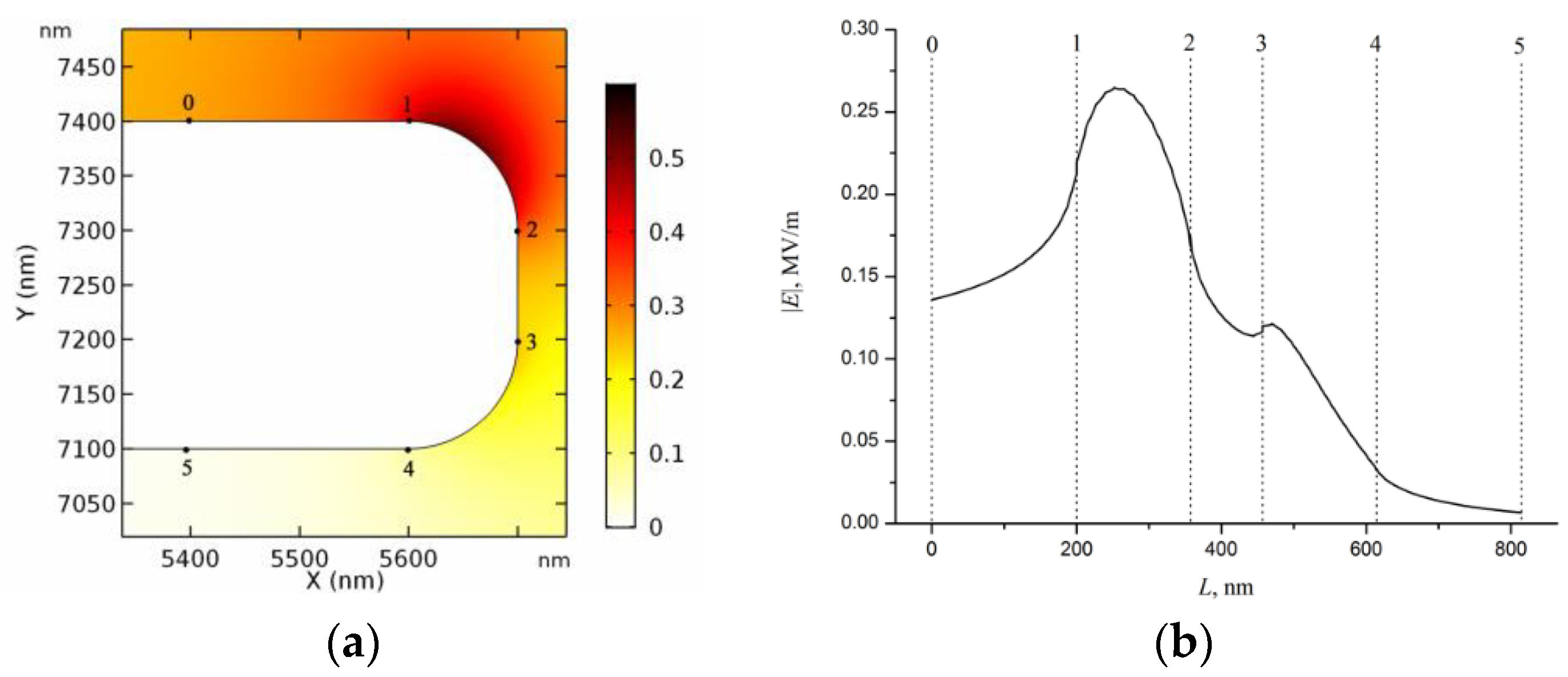
In particular, this evidence is provided by the results of numerical simulation of the function |E|2/|E0|2 built along the perimeter of the blade generator inside molybdenum (Figure 5a), and within the vacuum (Figure 5b) when exposed to light with different wavelengths. Here, Figure 5c,d show distribution of the modulus of electrostatic field intensity when applied to the gate of the potential Ug = 1 V (along the perimeter of the blade generator outside the emitter and a two-dimensional distribution near the tip of the emitter, respectively). The electrostatic field is also characterized by a certain degree of localization. However, the actual localization zone does not change the position compared with the spectral dependence of the position of optical field intensity extrema.
It is obvious that efficiency of the analyzed structure of the photosensor will improve if an additional adjustment element is introduced that ensures implementation of the matching principle to the localization zones of the absorbed optical and electrostatic fields.

3.3. A Model for the Tunnel Photocurrent within the Structure

In contrast to traditional metal photosensors with a flat radiation receiver, the surface of the sensitive element being investigated has a two-dimensional structure, where the depth of topological irregularities can be compared with the radiation wavelength. Therefore, as a result of the direct and reflected wave interference, we find a complex pattern of standing waves, particularly near the tip of the emitter blade (see Figure 2 and Figure 3). The calculations also showed that, when the emitter is irradiated by electromagnetic radiation of the visible or near IR range, the penetration depth of electromagnetic waves into the molybdenum blade (the skin depth) can be about 30 nm (distribution of the normalized specific absorption power at the depths up to 20 nm is shown in Figure 4). In this case, the diffraction effects of the fields in the vacuum form significant spatial inhomogeneity of the optical field and inside the emitter along the blade perimeter, as shown in Figure 4. This leads to substantial inhomogeneity of the specific absorption power not only along the depth of the skin layer, but also along the perimeter of the tip of the blade.
In the external strong electrostatic field, the height of the potential barrier over the metal surface decreases by
Δφ = (e3F)1/2 = 1.2 (F(V/nm))1/2,
where e is the absolute value of electron charge.
Then, the tunneling probability of the hot electrons from the emitter surface when exposed to optical radiation in both the visible and near-IR ranges increases exponentially. This happens despite the low photon energy, which is noticeably less than the work function φ0. The results provided in the recent works [5,12,13,25,26] demonstrate the experimental observation of the tunnel photoemission.
As follows from the analysis of strength distribution in the electrostatic field presented in Figure 5c,d, the localization zone in the emitter is limited to the part of the segment designated by the points 3 and 4. According to (3), it is only in this zone that the Schottky barrier decreases to the maximum, whereas the permeability increases, respectively, and conditions can arise for the tunneling of photoelectrons into the vacuum.
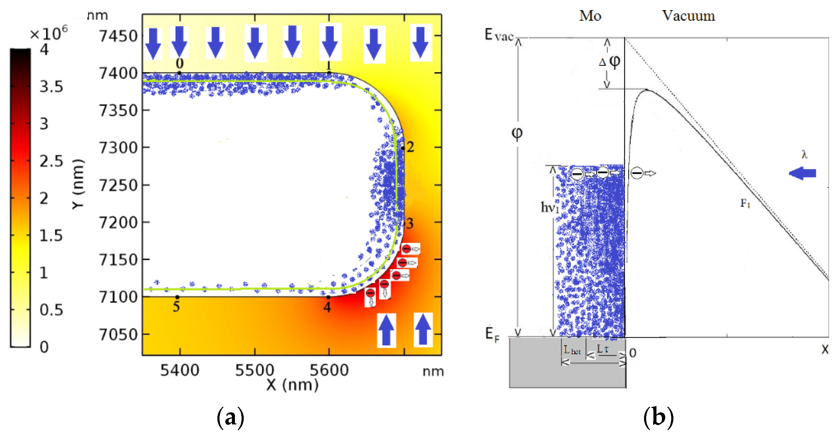
A generalized scheme and mechanisms for sequential irradiation of the tip of the blade, generation of hot electrons at the volume of the molybdenum emitter skin layer, the transport of hot electrons from the layer with Lτ thickness to the surface of the emitter, and their tunneling into the vacuum in the localization zone of the electrostatic field are given in Figure 6.
The probability of tunneling of nonequilibrium photoelectrons generated in the surface layer of molybdenum with the thickness Lτ with the energy EF + and the momentum directed normally to the surface of the emitter is determined by the following relationship [13,21]:
D λ = exp [ 8 π / 3 ( 2 m / h ) ( φ h ν ) 3 / 2 e F ϑ ( y ) ]
Here, is the energy of irradiating photons, y ≡ (e3F)1/2/(φ) is the relative decrease in the potential barrier height for nonequilibrium photoelectrons, ϑ ( y ) is the Nordheim elliptic function, the range of the argument variation is 1 > y 0 , m is the effective mass electron, and F is intensity of the electrostatic field.
Accounting of the temperature effects carried out in the work of [12] allowed us to obtain the relations needed to determine the tunneling probability of hot electrons that reach the surface of the emitter Pλ, and the tunneling photocurrent density IPh from the metal emitter depending on the electrostatic field F and the monochromatic light intensity Iλ.
P λ = h 2 F 2 β T 2 16 π m ( φ h ν ) G ( β T E F ) D λ ,
IPh = Iλ (e/) (1 − Rλ) Pλfλ (1 − exp(−αλL)),
where βT = 1/(kT); G is the Fowler function; Rλ = |(1 − nr)/(1 + nr)|2, where (nr)2 = εr (the relative permittivity of the metal); fλ is the coefficient taking into account the ratio of the free path Lτ of hot electrons to the absorption length of electromagnetic radiation at the wavelength λ; αλ is the absorption coefficient, and L is the molybdenum blade thickness.
It follows from relations (4)–(6) that the photocurrent of hot electrons depends exponentially on the electrostatic field. This pattern is similar to the dependence of the field emission on the strength of the local field. At the same time, the photocurrent of the hot electrons increases linearly with an increase in intensity of the detected optical radiation.
A new design of the photosensor modernized by introducing an additional electrode from the opposite side of the gate will broaden the possibilities to influence the configuration and position of the electrostatic field localization zone (the second type). To make the influence of the potential Ua on the additional control electrode significant, it is necessary to ensure a relatively small gap between the electrode and the plane of the emitter. There is experience in manufacturing the structures of the given type [27,28]. To make it clear, let us set the gap at 5 nm when simulating a transformed electrostatic field.
As can be seen in Figure 7a,b, application of a unit potential to an additional electrode leads to the appearance of the localization zone of the electrostatic field on the surface of the upper curve of the emitter blade and its end portion. However, the amplification level of the local field is noticeably lower than when the same unit potential is applied to the gate. This conclusion follows from comparing the data relating the field strength in Figure 5c,d (on the fragment of the boundary surface between the points 3 and 4) on the lower rounding with relevant data relating the field strength in Figure 7a,b on the upper rounding (between the points 1 and 2). Therefore, approximately equivalent enhancement of the field strength with control of both electrodes is achieved when the potential ratio Ua/Ug is equal to 4. The results of the calculation of the field strength distribution for the given potential ratio are shown in Figure 7c,d, where both the expansion of the area of the localization zone and the increase in the maximum field strength are demonstrated simultaneously. The calculation examples provided in Figure 6 and Figure 8 demonstrate the possibilities for the changes within a wide range of topology and position of electrostatic localization zones, as well as the maximum field level within the zones.

3.4. Design of the Experiment

A response of the photosensor prototype was experimentally studied using repetitively pulsed laser radiation with a tunable wavelength. An automated optical parametric oscillator LT-2214-PC pumped by a multi-harmonics Nd/YAG laser was applied as the radiation source (both units are the products of the “Lotis TII” company, Minsk, the Republic of Belarus). The converted laser beam passed through a concave quartz lens with the focal length equal to 50 mm. After the lens, the diverging laser beam fell onto the sensor surface placed at the distance of 150 mm from the lens. The diameter of light spot at the sensor surface was equal to 7 mm. The angle of laser beam incidence onto the sensor surface was approximately equal to 85° and the part of retro-reflected beam was used to evaluate the average power of laser irradiation with a Maestro power meter (the product of Gentec Electro-Optics, Inc., Quebec city, QC, Canada). Before experiments, the setup was calibrated in order to estimate the average power of laser light reaching the sensor surface. The experimental study was carried out with the following parameters of laser irradiation: the wavelength varied from 420 nm to 700 nm and from 800 nm to 1064 nm; the pulse duration was equal to 10 ns; the repletion rate was equal to 10 Hz; and the energy of laser pulses reaching the sensor surface varied between 2 mJ and 12 mJ. This corresponds to the optical power density of the laser beam in a pulse of 50–300 kW/cm2.

3.5. Results of the Experimental Study and Their Interpretation

Spectral dependence of the photo-sensor response was recovered using the experimental data obtained in the accordance with the above subsection. The switch-on mode of the device corresponded to that shown in Figure 5, when a single electrode, a gate, was used for controlling. Analysis of the measurement results in Figure 8a, performed at various levels of the gate potential, shows that an increase in the electrostatic field strength leads to a noticeable increase in the photon emission with the wavelength ranging between 520–580 nm. A two-fold increase in the photocurrent is achieved with a slight increase (about 3%) in electrostatic field strength. Regarding the rest of the investigated range of the wavelength of irradiating laser, a growth in the photocurrent is also observed, though it is less evident. It is necessary to notice an increased irregularity of the spectral curves in Figure 8a. The laser with a tunable working wavelength used in the experiment has a spectral dependence of the pulse energy, as shown in Figure 8b, and a gap ranging within 700–800 nm. During the tests in the available range of tuning of the near-infrared radiation (from 800 to 1064 nm), 0.2–0.8 µA photocurrent of the vacuum sensor under laser pulse irradiation of 0.2–0.5 mJ was also detected.
In our view, the observed regularities of the far-field diffraction effect of the optical wave at the submicron scale stage (emitter—gate) on significant phase dispersion in the amplitude and direction of the Poiting vector over the molybdenum emitter surface (see simulation results in Figure 5) provide an adequate interpretation of the experimentally observed processes. The position of localization zones of the specific optical signal absorption power, on the one hand, and unchanging position of the electrostatic field localization zone, on the other hand, which rapidly change with the frequency of the irradiating beam, lead to their asynchronous behavior. A lack of coordination of the two types of localization zones (optical absorption and electrostatic external field) relating the mutual position results in the decrease of the photo-sensor response within a relatively narrow frequency range. With a further change in the radiation wavelength, there conditions are favorable for both the absorption and tunneling of hot electrons into the vacuum.
Under such conditions, an emerging possibility for an additional adjustment of the system by varying positions of electrostatic field localization zones and changing the potential of control electrodes, as shown in Figure 7, ensures the prospect for improving the vacuum photosensor parameters.
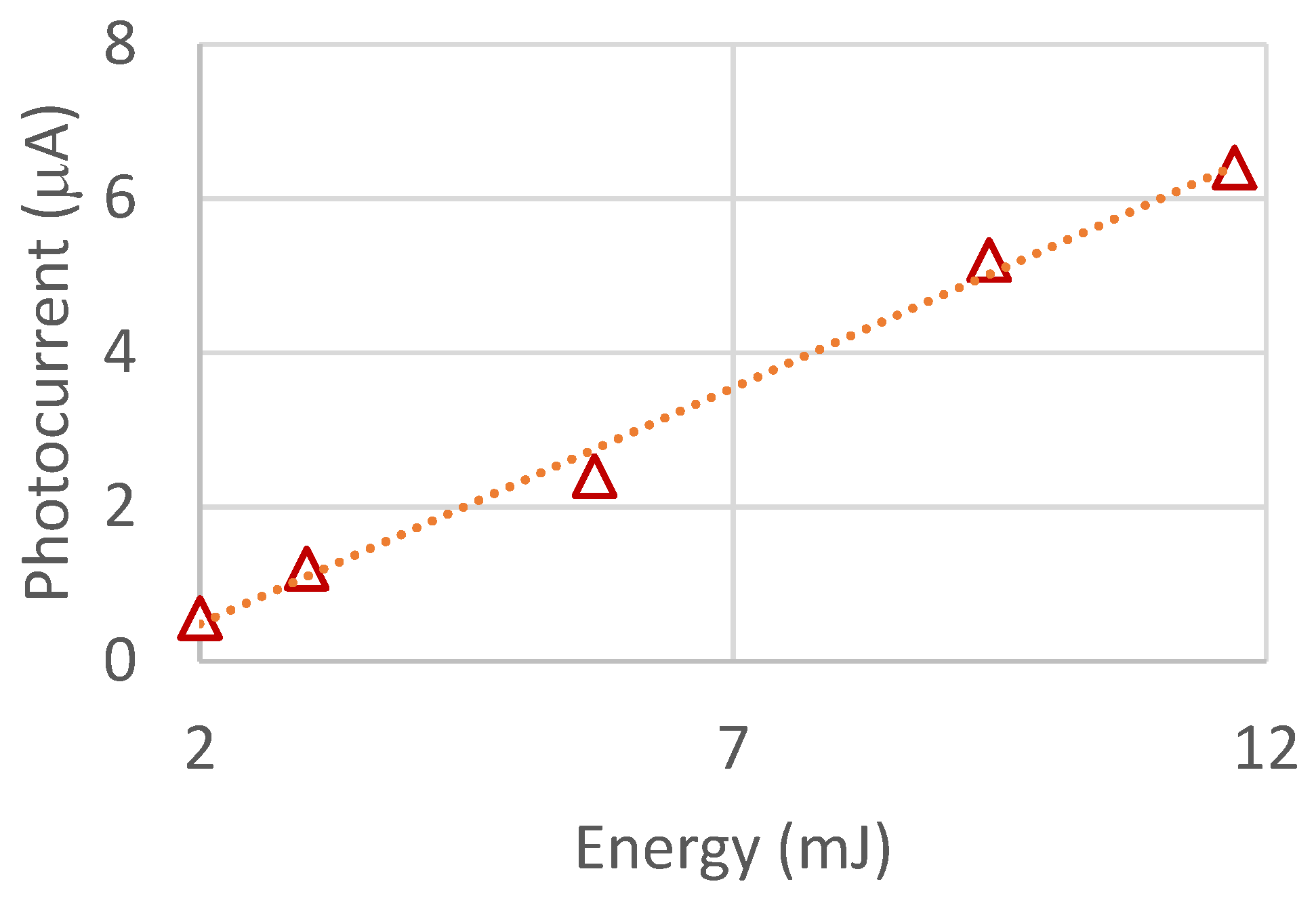
The illustrated possibility that ensures the performance of the vacuum photosensor in a wide wavelength range (ranging from the visible up to near infrared radiation) is explained by a single photon effect of the tunnel photoemission process. To prove the performance reliability, we provide the measurements of the photocurrent as the function of the laser pulse energy. Linearity of the dependence designed in Figure 9 indicates the absence of nonlinear processes characteristic of the multiphoton photoemission. This allows us to predict a possibility to further upgrade the efficiency of the tunnel photoemission.
Note the structure of a 1 µm cell period with the localization of the electrostatic field [5], the measured photo current rates for the fixed bias voltages showed a significant non-linear increase with an increase in the optical power. In our view, the reason for such photo current behavior could be extremely high levels of the form-factor and small inter-tip distances. As a result of intensified near-field effects (localization of the optical field on the nanoscale tips), redistribution of the concentration of hot electrons can lead to the nonlinear effects of electron–electron and electron–phonon interactions. Linearity of the photo current-optical power characteristics of the proposed and investigated photosensor is estimated as preferable for the majority of optical-electronic applications.
Known devices based on arrays of gold plasmon nanosized elements can be mentioned as similar photosensors: in the form of “mushrooms” [6] and in the form of a triangular unit-cell on adjacent rows [5]. In both cases, the effect of local surface plasmon resonance of gold nanostructures is used. On the basis of a theoretical analysis, the above studies show that the electric field enhancement can reach 100–120 only at certain resonant frequencies. The experimental data on the study of the photoeffect in a vacuum diode are presented for two wavelengths of 633 and 785 nm in the work of [6] and for one value λ = 785 nm in the work of [5]. A feature of the nanostructure [5] is a very small vacuum gap between adjacent opposite points, which is 50 nm. The photoeffect is observed while ensuring the electric field in the gap at a level of up to 1 GV/m. When the field was varied, a photocurrent of 0.3–8 μA was detected upon irradiation with a laser beam with an intensity of 0.2 kW/cm2. The analysis of the results of the study of the photosensor in this article allows us to determine the intensity of the working field. The photoeffect is detected at a field of 0.22–0.24 GV/m. The magnitude of the photocurrent in this case varies in the range 0.3–5.8 μA (see Figure 8a), which approximately corresponds to the level of the photoresponse of the analog [5].
Along with the broadband of the studied photosensor, it is necessary to note the following additional advantages in comparison with analogues:
(i)
The simplicity and low cost of manufacturing technology (traditional photolithography compared with e-beam lithography, molybdenum instead of gold).
(ii)
The “open” structure of the photosensor electrodes allows the formation of a directed electron flow from the tip of the blade into the free space. This is important for creating current sources for vacuum devices (X-ray tubes, UHF (Ultra high frequency) and THz (Terahertz) generators, and amplifiers) with ultrafast optical signal modulation. In known analogues with nanoscale vacuum gap, the possibility of forming an electron flow with a controlled trajectory is associated with great difficulties.

4. Conclusions

Thus, it is shown that a two-level system of electrodes with a submicron gap provides favorable possibilities for localization of the electrostatic field on the tip of the molybdenum blade and ensures efficient tunnel photoemission into the vacuum within a wide wavelength range (visible radiation and near IR).
An investigation, on the basis of theoretical analysis, of the interaction characteristic of the incident optical radiation with the blade structure proves the existence of two types of nanoscale localization that must be taken into account when designing the vacuum photosensors with a metal nanoscale sensitive element. The results of the experiments to study the spectral dependence of the response confirm the conclusions of theoretical investigations.
The results of theoretical and experimental studies demonstrate the expanding range of the single-photon tunnel photosensitivity of the vacuum metal sensor from the near UV to the near IR.
The proposed method of implementing the matching principle for localization zones of the hot electrons and a strong electrostatic external field provides the prospect to improve the parameters of the vacuum photosensors. The described photosensors, owing to a possibility of ballistic transport of photoelectrons in the vacuum gap with a high electrostatic field intensity, are candidates for creating ultrafast applications, including optoelectronic modulators of electron beams, ultrafast photodetectors, and terahertz radiation generators.

Author Contributions

D.Z. and A.Y. conceived and designed the theoretical investigations and experiments; N.A. supervised all aspects of photosensor fabrication; G.A., S.Y., S.V., and A.L. fabricated the samples and performed measurements. Y.A., G.A., S.Z., and A.Y. developed the physical and computational models and performed calculations. All authors contributed to scientific discussions and manuscript writing and editing.

Funding

This research was funded by the Russian Foundation for Basic Research (project No. 19-07-00378) in the part of photosensor fabrication and measurements performing, by the Ministry of Science and Higher Education of the Russian Federation (project AAAA-A18-118042790042-4) in the part of development of physical and computational models. D.Z. thanks the Ministry of Education and Science of the Russian Federation (project 3.7567.2017) for support of this work in the part of design of the experimental setup. S.V. acknowledges the support from the Russian Foundation for Basic Research (project No. 19-32-90221) in the part of experimental studies.

Conflicts of Interest

The authors declare no conflict of interest.

References

  1. Brongersma, M.L.; Halas, N.J.; Nordlander, P. Plasmon-induced hot carrier science and technology. Nat. Nanotechnol. 2015, 10, 25–34. [Google Scholar] [CrossRef] [PubMed]
  2. Goykhman, I.; Desiatov, B.; Khurgin, J.; Shappir, J.; Levy, U. Waveguide based compact silicon Schottky photodetector with enhanced responsivity in the telecom spectral band. Opt. Expess 2012, 20, 28594–28602. [Google Scholar] [CrossRef] [PubMed]
  3. Wei, L.; Valentine, J. Metamaterial Perfect Absorber Based Hot Electron Photodetection. Nano Lett. 2014, 14, 3510–3514. [Google Scholar] [CrossRef]
  4. Pu, H.; Kamruzzaman, M.; Sun, D.-W. Selection of feature wavelengths for developing multispectral imaging systems for quality, safety and authenticity of muscle foods-a review. Trends Food Sci. Technol. 2015, 45, 86–104. [Google Scholar] [CrossRef]
  5. Piltan, S.; Sievenpiper, D. Plasmonic Nano-arrays for Enhanced Photoemission and Photodetection. JOSA B 2018, 35, 208–213. [Google Scholar] [CrossRef]
  6. Forati, E.; Dill, T.J.; Tao, A.R.; Sievenpiper, D. Photoemission-based microelectronic devices. Nat. Commun. 2016, 7, 13399. [Google Scholar] [CrossRef] [Green Version]
  7. Saidaminov, M.I.; Adinolfi, V.; Comin, R.; Abdelhady, A.L.; Peng, W.; Dursun, I.; Yuan, M.; Hoogland, S.; Sargent, E.H.; Bakr, O.M. Planar-integrated single-crystalline perovskite photodetectors. Nat. Commun. 2015, 6, 8724. [Google Scholar] [CrossRef] [Green Version]
  8. Mak, K.F.; Shan, J. Photonics and optoelectronics of 2D semiconductor transition metal dichalcogenides. Nat. Photonics 2016, 10, 216–226. [Google Scholar] [CrossRef]
  9. Buscema, M.; Groenendijk, D.J.; Blanter, S.I.; Steele, G.A.; van der Zant, H.S.J.; Castellanos-Gomez, A. Fast and Broadband Photoresponse of Few-Layer Black Phosphorus Field-Effect Transistors. Nano Lett. 2014, 14, 3347–3352. [Google Scholar] [CrossRef] [Green Version]
  10. Huang, J.-A.; Luo, L.-B. Low-Dimensional Plasmonic Photodetectors: Recent Progress and Future Opportunities. Adv. Optical Mater. 2018, 6, 1701282. [Google Scholar] [CrossRef]
  11. Zhang, Z.; Wang, K.; Zheng, K.; Deng, S.; Xu, N.; Chen, J. Electron Bombardment Induced Photoconductivity and High Gain in a Flat Panel Photodetector Based on ZnS Photoconductor and ZnO Nanowire Field Emitters. ACS Photonics 2018, 5, 4147–4155. [Google Scholar] [CrossRef]
  12. Forati, E.; Sievenpiper, D. Electron emission by long and short wavelength lasers: Essentials for the design of plasmonic photocathodes. J. Appl. Phys. 2018, 124, 083101. [Google Scholar] [CrossRef]
  13. Aban’shin, N.P.; Akchurin, G.G.; Avetisyan, Y.A.; Loginov, A.P.; Mosiyash, D.S.; Yakunin, A.N. Tunnel electron photoemission in the nanoscale DLC film structure with electrostatic field localization. Proc. SPIE 2017, 10337, 1033707. [Google Scholar] [CrossRef]
  14. Aban’shin, N.P.; Avetisyan, Y.A.; Akchurin, G.G.; Loginov, A.P.; Morev, S.P.; Mosiyash, D.S.; Yakunin, A.N. A planar diamond-like carbon nanostructure for a low-voltage field emission cathode with a developed surface. Technical Phys. Lett. 2016, 42, 509–512. [Google Scholar] [CrossRef]
  15. Foiles, C.L. Drude parameters of pure metals. In Electrical Resistivity, Thermoelectrical Power and Optical Properties; Hellwege, K.-H., Olsen, J.L., Eds.; Springer: Berlin/Heidelberg, Germany, 1985; pp. 212–222. ISBN 978-3-540-11694-3. [Google Scholar]
  16. Abrikosov, A.A. Fundamentals of the Theory of Metals, Dover Edition; Dover Publications Inc.: New York, NY, USA, 2017; pp. 115–117. ISBN 0486819019. [Google Scholar]
  17. Einstein, A. Übereinen die Erzeugung und Verwandlung des Lichtes betreffenden heuristischen Gesichtspunkt. Ann. Phys. 1905, 322, 132–148. [Google Scholar] [CrossRef]
  18. Fowler, R.H. The analysis of photoelectric sensitivity curves for clean metals at various temperatures. Phys. Rev. 1931, 38, 45–56. [Google Scholar] [CrossRef]
  19. Ordal, M.A.; Bell, R.J.; Alexander, R.W.; Newquist, L.A.; Querry, M.R. Optical properties of Al, Fe, Ti, Ta, W, and Mo at submillimeter wavelengths. Appl. Opt. 1988, 27, 1203–1209. [Google Scholar] [CrossRef]
  20. Gao, L.; Lemarchand, F.; Lequime, M. Refractive index determination of SiO2 layer in the UV/Vis/NIR range: spectrophotometric reverse engineering on single and bi-layer designs. J. Europ. Opt. Soc. Rap. Public. 2013, 8, 13010. [Google Scholar] [CrossRef] [Green Version]
  21. Nolle, E.L. Tunneling photoeffect mechanism in metallic nanoparticles activated by cesium and oxygen. Physics Uspekhi 2007, 50, 1079–1082. [Google Scholar] [CrossRef]
  22. Chang, L.; Besteiro, L.V.; Sun, J.; Santiago, E.Y.; Gray, S.K.; Wang, Z.; Govorov, A.O. Electronic Structure of the Plasmons in Metal Nanocrystals: Fundamental Limitations for the Energy Efficiency of Hot Electron Generation. ACS Energy Lett. 2019, 4, 2552–2568. [Google Scholar] [CrossRef]
  23. Akchurin, G.G.; Zimnyakov, D.A.; Aban’shin, N.P.; Akchurin, G.G., Jr.; Avetisyan, Y.A.; Loginov, A.P.; Yuvchenko, S.A.; Zarkov, S.V.; Yakunin, A.N. Spectral and polarization characteristics of a broadband vacuum photosensor with tunnel emission from a metal nanoscale blade. Proc. SPIE 2019, 11066, 110660A. [Google Scholar] [CrossRef]
  24. Khorashad, L.K.; Besteiro, L.V.; Wang, Z.; Valentine, J.; Govorov, A.O. Localization of Temperature Using Plasmonic Hot Spots in Metal Nanostructures: The Nano-Optical Antenna Approach and Fano Effect. J. Phys. Chem. C 2016, 120. [Google Scholar] [CrossRef] [Green Version]
  25. Tsujino, S.; Beaud, P.; Kirk, E.; Vogel, T.; Sehr, H.; Gobrecht, J.; Wrulich, A. Ultrafast electron emission from metallic nanotip arrays induced by near infrared femtosecond laser pulses. Appl. Phys. Lett. 2008, 92, 193501. [Google Scholar] [CrossRef] [Green Version]
  26. Akchurin, G.G.; Yakunin, A.N.; Aban’shin, N.P.; Gorfinkel’, B.I.; Akchurin, G.G., Jr. Controlling the Red Boundary of the Tunneling Photoeffect in Nanodimensional Carbon Structures in a Broad (UV–IR) Wavelength Range. Tech. Phys. Lett. 2013, 39, 544–547. [Google Scholar] [CrossRef]
  27. Yakunin, A.N.; Aban’shin, N.P.; Mosiyash, D.S.; Avetisyan, Y.A.; Akchurin, G.G. Features of field emission and formation of electron beam in a multi-electrode planar cathode. In Proceedings of the 2018 International Conference on Actual Problems of Electron Devices Engineering (APEDE), Saratov, Russia, 27–28 September 2018; Amirit Co. Ltd.: Saratov, Russia, 2018; pp. 249–252. [Google Scholar] [CrossRef]
  28. Yakunin, A.N.; Aban’shin, N.P.; Avetisyan, Y.A.; Akchurin, G.G.; Akchurin, G.G., Jr.; Loginov, A.P.; Morev, S.P.; Mosiyash, D.S. Stabilization of Field- and Photoemission of a Planar Structure with a Nanosized Diamond-Like Carbon Film. J. Commun. Technol. Electron. 2019, 64, 83–88. [Google Scholar] [CrossRef]
Figure 1. A photosensor (a) in the vacuum housing with a planar glass molybdenum blade structure; (b) the top view of the parallel blade system; (c) the computational domain (with a half-period of 16.5 μm) for constructing a finite element model of a section of a blade emitter—(1) molybdenum emitter, with the thickness of 300 nm and potential of 0 V; (2) dielectric layer of SiO2, with the thickness of 700 nm; (3) molybdenum gate with the potential Ug; (4) vacuum.
Applsci 09 05356 g001
Figure 2. Normalized distributions of the squared modulus of the complex total electric field vector |E|2/|E0|2 in the analyzed structure, where E0 is the complex electric field vector of the illuminating beam at the wavelength of (a) 500 nm and (b) 700 nm.
Applsci 09 05356 g002
Figure 3. Spatial distributions of the normalized squared modulus of the electric field vector |E|2/|E0|2 near the emitter in the vacuum (right tone scale) and inside the molybdenum emitter (left tone scale). The wavelength of the irradiating light is (a) 430 nm, (b) 500 nm, and (c) 550 nm.
Applsci 09 05356 g003
Figure 4. Spectral dependences of the normalized specific absorption power of optical radiation over the surface and different depths (0, 2, 6, 10, and 20 nm) inside the molybdenum emitter, estimated in the vicinity of point 2 indicated in Figure 3.
Applsci 09 05356 g004
Figure 5. Dependencies of the squared modulus of the optical field along the generatrix 0–5 of the emitter molybdenum blade section inside (a) and outside (b) the surface; dependence of electrostatic field at the unit potential Ug along the perimeter of the generatrix 0–5 (c) and a two-dimensional vicinity of the emitter blade tip (d).
Applsci 09 05356 g005aApplsci 09 05356 g005b
Figure 6. (a) Two-dimensional schematic image of the tip of the emitter nano-edge irradiated by the optical beam (blue arrows from top to bottom), and reflected radiation from the gate (blue arrows from bottom to top), uneven formation of hot electrons (blue dots) both across the depth of the skin layer and across the emitter perimeter (occurrence of spatial localization zones at each given irradiation wavelength); tunneling of hot electrons into the vacuum in the localization zone of the external strong electrostatic field (the scale of the electrostatic field strength is on the left). (b) Diagram of the energy levels in the metal within a strong external electrostatic field when the emitter surface is irradiated with optical radiation (blue arrow) with the photon energy less than the outcoming energy of electrons φ equal to the difference between the energy in the vacuum level and the Fermi level; probability of electron tunneling depends exponentially on the electron energy (EF for the field emission, and EF + for the photoemission) and the height of the potential barrier, which decreases in the strong electrostatic field by (3).
Applsci 09 05356 g006
Figure 7. Dependence of the electrostatic field strength at the unit potential Ug in the vicinity of the tip of the emitter blade (a) and along the perimeter of the generatrix 0–5 (b); (c,d), the same in the case when the potentials are applied to both control electrodes of the photosensor Ug = 1 V and Ua = 4 V.
Applsci 09 05356 g007aApplsci 09 05356 g007b
Figure 8. Spectral dependence of the sensor response at two levels of the gate potential Ug—158 V and 170 V (a); laser pulse energy dependence vs. wavelength (b).
Applsci 09 05356 g008
Figure 9. Dependence of the photocurrent of the vacuum sensor with a molybdenum blade sensing element on the laser pulse energy; the wavelength of the irradiating beam is 540 nm.
Applsci 09 05356 g009