Article

Classic Discrete Control Technique and 3D-SVPWM Applied to a Dual Unified Power Quality Conditioner

by
Y. A. Garces-Gomez
1,*,
Fredy E. Hoyos
2 and
John E. Candelo-Becerra
3
1
Academic Training Unit in Natural Sciences and Mathematics, Universidad Católica de Manizales, Cra 23 No. 60-63, Manizales 170001, Colombia
2
School of Physics, Faculty of Science, Universidad Nacional de Colombia-Sede Medellín, Carrera 65 No. 59A-110, Medellín 050034, Colombia
3
Department of Electrical Energy and Automation, Faculty of Mines, Universidad Nacional de Colombia-Sede Medellín, Carrera 80 No 65-223, Campus Robledo, Medellín 050041, Colombia
*
Author to whom correspondence should be addressed.
Appl. Sci. 2019, 9(23), 5087; https://doi.org/10.3390/app9235087
Submission received: 29 October 2019 / Revised: 9 November 2019 / Accepted: 14 November 2019 / Published: 25 November 2019
(This article belongs to the Section Electrical, Electronics and Communications Engineering)

Abstract

:
The unified power quality conditioners (UPQCs) are useful to correct distortions in voltage and current waveforms in case of problems related to harmonics, flicker, and power factor. The dual topology of the UPQC allows a loop control in the inverters less demanding in terms of switching functions; however, the control techniques proposed in the literature have some disadvantages as large computation time and some calculation delays. Therefore, this paper presents the application of a classic discrete-time control model for a three-dimensional space vector pulse width modulation (3D-SVPWM) to be used with the dual UPQC, obtaining a fixed commutation frequency and a low computation cost. The results show that the applied method helps to reduce the harmonics in the source, voltage sags and load current and improve the power factor of the electrical circuit tested. Furthermore, the high frequency created by the switching of elements in the UPQC is filtered by the impedance of the power source and it does not represent a problem for the circuit. Due to the simplicity of the model, simulations demonstrate that the application of this classical control technique is enough to achieve good results to compensate harmonics and power factor with the dual UPQC. The development of the controllers is carried out by discretization of the transfer functions of the control in continuous time and their application with the three-dimensional space vector pulse width modulation (3D-SVPWM) technique.

1. Introduction

Most efforts to improve power system operation are focused on using the most advanced technical solutions such as flexible AC transmission systems (FACTS) [1,2], and for distribution networks, there is a wide variety of options that includes series and shunt compensators to improve power quality or reduce harmonics problems [3,4]. Therefore, the unified power quality conditioner (UPQC) is considered as a good solution because it gives versatility when compensating several problems simultaneously [5].
An UPQC consists of two power inverters operating as active filters that share the same direct current (DC) bus [6,7,8,9,10,11]; and they are widely used as energy controllers [12,13,14,15]. The active power filters (APFs) are connected to the power system generally by means of coupling inductors for the shunt active power filters (shunt APF), and coupling transformers for the series active power filters (series APF). Both the shunt and the series inverters operate as controlled voltage or current sources in the system, mitigating the effects of power quality problems such as voltage and current harmonics, voltage sags, momentary voltage swells, flicker, unbalanced source, and unbalanced load.
The schematic diagram of the UPQC is presented in Figure 1 [16,17,18], where the series and shunt APFs are used to improve the harmonics. The term i i a , i i b , and i i c are the currents of the main electrical circuit that considers the source and load, which is supplied through phases a, b, and c, respectively; R r d a , R r d b , and R r d c are the resistances of the power grid in phases a, b, and c, respectively; L r d a , L r d b , and L r d c are the inductances of the power grid in phases a, b, and c, respectively; V B is the DC link voltage; C b 1 and C b 1 are the corresponding capacitors in the DC bus; i c s a , i c s b , and i c s c are the currents of the series APF in phases a, b, and c, respectively; i c p a , i c p b , and i c p c are the currents of the shunt APF in phases a, b, and c, respectively; L s a , L s b , and L s c are the inductances of the series APF in phases a, b, and c, respectively; and finally, L p a , L p b , and L p c are the inductances of the shunt APF, in phases a, b, and c.
The traditional topology and the dual topology of the UPQC have identical devices in their circuit configuration, as shown in Figure 2 and Figure 3. Thus, the traditional topology of the UPQC considers a series of APF that work as a controlled voltage source and a shunt APF that works as a controlled current source (see Figure 2). On the other side, the filters in the dual topology of the UPQC are interchanged and now the shunt APF works as a controlled voltage source and the series APF works as a controlled current source [19,20,21,22,23] (see Figure 3); where the terms v f and i f are the controlled voltage and current sources of the APFs, respectively.
The main advantage of the dual topology of the UPQC lies in the loop control of the inverters. In the traditional UPQC model, the voltage and current reference signals are highly distorted, and consequently, the control effort in power devices is considerable when trying to generate these distorted waveforms. On the other hand, in the dual UPQC, the compensation voltage references are pure sinusoidal, which allows a less demanding in the inverters in terms of switching frequency.
The use of UPQCs in distribution networks and their performance analyses are widely found in the literature. For example, in [24] the authors verify the static and dynamic performance of the power quality conditioners PQC operating as UPQC. Besides, in [25], authors propose the use of three isolated H-bridge with a voltage source at the DC side of series active power filter with capability to protect sensitive loads against harmonics, sags, swells and unbalances of the power system voltages. Furthermore, in [17], the authors present an experimental evaluation of a digital control system based on a dual digital signal processor architecture for a three-phase UPQC; where the results show the minimization of delays caused by the processing time and the increment of the UPQC performance.
On the other side, several control techniques have been proposed in the literature [5], such as the based on artificial neural networks to separate the harmonics in the nonlinear load [26,27], which can present delays and large computation time. Other authors have used wavelet analysis techniques to represent a time-varying signal to control the UPQC [5], such as in [28] where a control strategy is proposed to extract the compensating signals for the control of series and shunt converters of the UPQC, or in [29] where it is used for power quality improvement with the UPQC. Other techniques based on pq and dq theories have been proposed [5], such as in [30] where the authors proposed a solution for power quality issues with the UPQC under-voltage and load unbalances conditions; or in [31], where the authors use a UPQC to inject a minimum active power and with limitations in the rated voltage capacities of the series compensators and the phase difference during voltage sags events; however these techniques use low pass and high pass filters that can affect the performance of the controller [5].
The literature shows that the UPQC has been used to improve power quality and the harmonics of the system; however; the control techniques have some disadvantages as large computation time and calculation delays. Therefore, this paper presents the application of a classic discrete-time control model for a three-dimensional space vector pulse width modulation (3D-SVPWM). The proposed control technique enables the UPQC to isolate the load from a harmonic-contaminated power supply and the momentary variations of the signals. At the same time, the current harmonics are eliminated and the power factor of the load is corrected, generating an ideal system at the common connection point. The designed model allows us to quickly implement the control technique as a prototyping system with a low computational cost. The classic discrete-time control has the advantage of obtaining a fixed commutation frequency [32] what for industrial application helps to reduce audible noise, size of electrical equipment, eliminate subharmonics in the output signal, and others. Besides, PID controllers are developed for the series APF, shunt APF, DC bus voltage, DC bus unbalance voltage, and PWM.
The rest of the document is divided into four more sections. Section 2 describes the UPQC in dual topology, defining the detailed models of the series and shunt APFs. Section 3 presents the discrete controllers designed in the frequency domain and the 3D-SVPWM. Section 4 presents the results obtained from the application of the dual UPQC to a three-phase system. Finally, Section 5 presents the conclusions of the document.

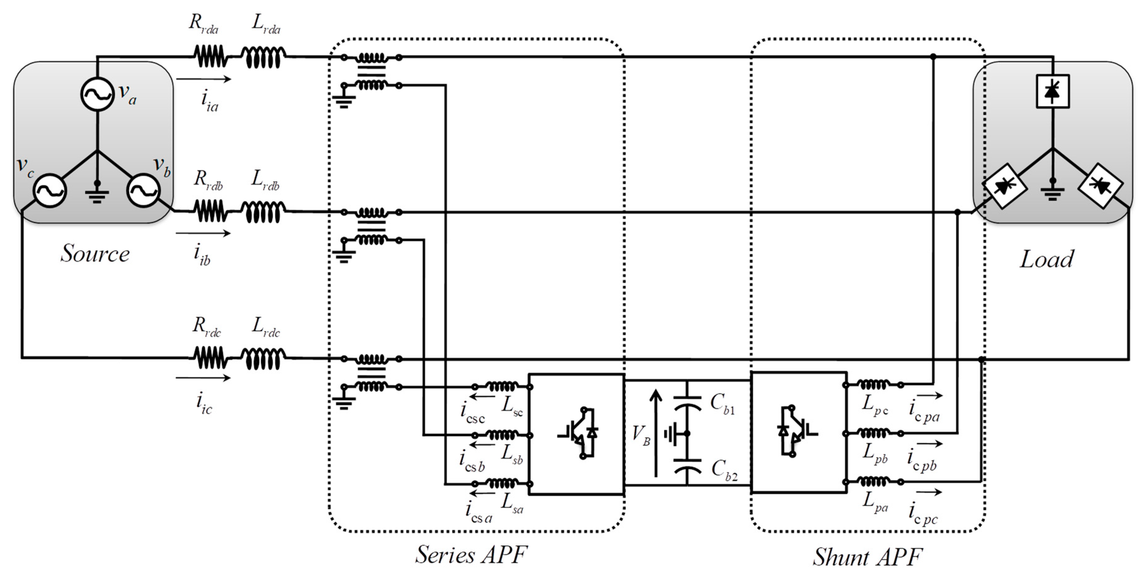
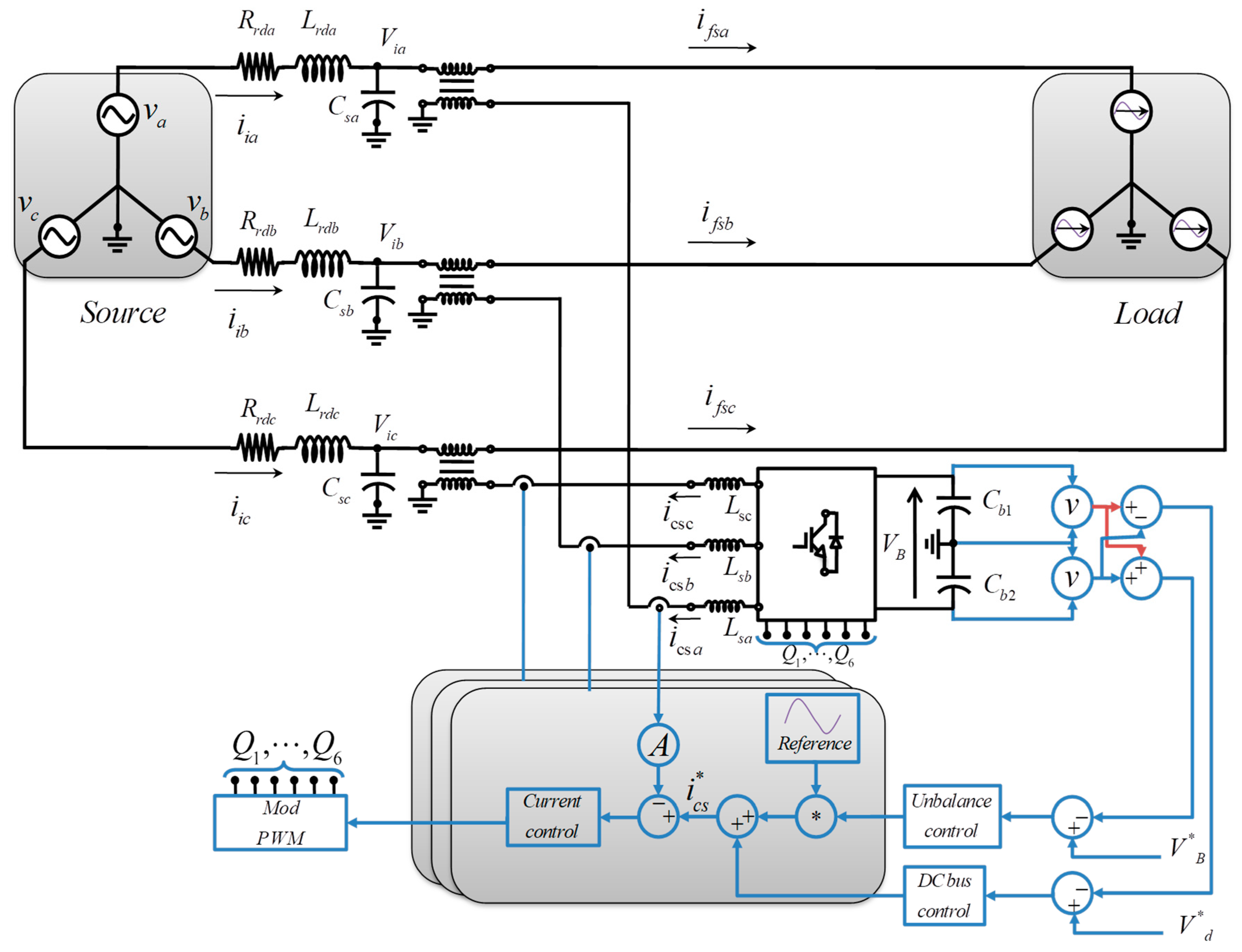
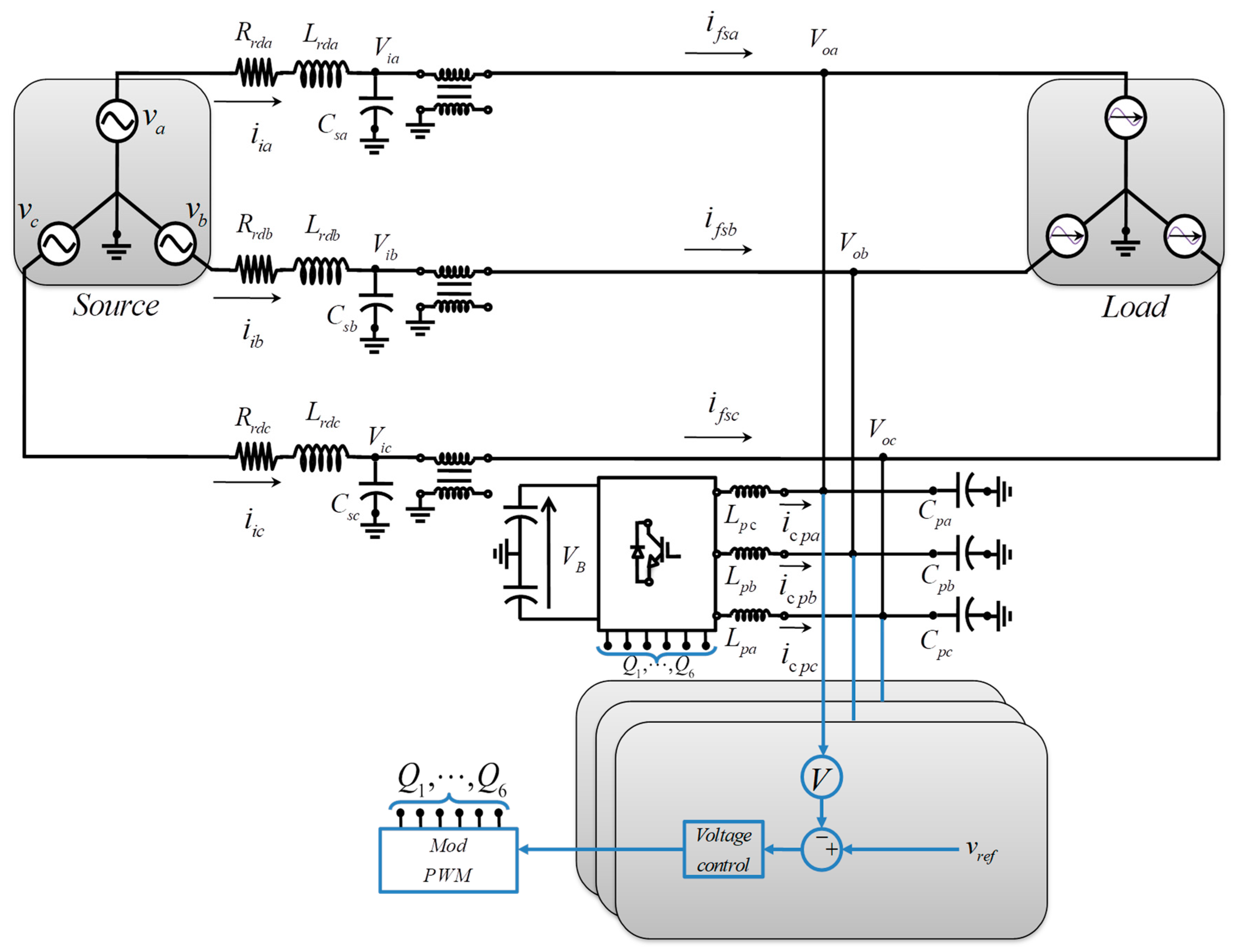
2. UPQC in Dual Topology

To model the UPQC, the split capacitor configuration in the DC bus was selected, allowing to develop each three-phase inverter like three independent single-phase inverter. Furthermore, series and shunt APFs were considered in the UPQC model.

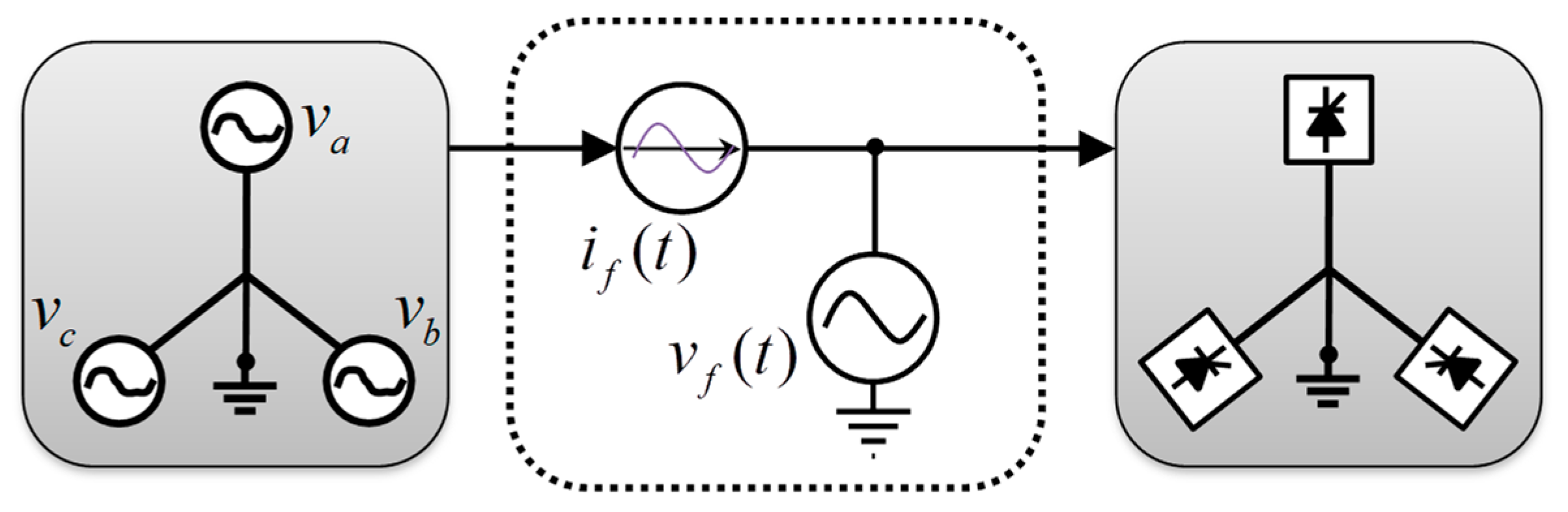
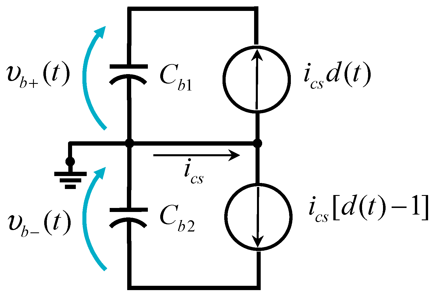
2.1. Series Active Power Filter (Series APF)

The simplified circuit in Figure 4 represents the series APF of the UPQC. Additionally to the terms defined in Section 1 for Figure 1, V i a , V i b , and V i a are voltages in the power grid between the series compensator and the network for phases a, b, and c, respectively; C s a , C s b , and C s c are the power grid capacitance of phases a, b, and c, respectively; and i f s a , i f s b , and i f s c are the filtered currents supplied to the load using the series APF. Moreover, Q 1 Q 6 are the duty cycles for the three-phase inverter; V d * is a reference for the unbalance voltage between the two DC capacitors; V B * is a reference for the DC link voltage; and i c s * is a reference for the current supplied by the series APF.
From the control scheme, there are three control loops. The first control loop corresponds to the current in the source side, responsible for controlling independently the current of each phase in the source. The second control loop corresponds to the voltage in the DC bus of the inverter to keep constant the voltage. The third control loop is required because of the DC branch that divides capacitors, and it is used to maintain the same voltage values in capacitors.
The block diagram in Figure 5 represents the control system of the series APF, which illustrates the three control loops previously mentioned only for phase a; this diagram is the same for phases b and c. Herein, V B * ( t ) is the required voltage in the DC bus of the power inverter applied as a reference with positive and negative values, according to the requirements in the capacitors of more or less energy drained through bi-directional inverter. Besides, the term H v is a voltage sensor gain. Furthermore, inside the “phase A control loop” the term H i represents the current sensor gain, V m is the PWM gain, G i ( s ) is the current loop transfer function, and K i is the current sensor gain ( K i = 0.44 ). Moreover, H d is the unbalanced voltage sensor gain, G d represents the unbalanced voltage transfer function, G v refers to the voltage loop transfer function, K v is the voltage control attenuation ( K v = 0.64 ), and K d denotes the unbalanced voltage control attenuation ( K d = 319 ). Finally, the output of the circuit is represented by two voltages: V d that refers to the unbalance voltage between two DC capacitors and V B defined as the DC link voltage.
The unbalance voltage is expected to have a small value so it can be neglected. Finally, the current reference is a sinusoidal signal synchronized with the fundamental frequency of the power network, so the load in conjunction with the series APF behaves as a pure resistive load.
The split capacitor configuration has several advantages. From the circuit point of view, a midpoint that allows correcting the unbalanced current of the load. From the modeling point of view, three independent single-phase inverters that allow analyzing the three-phase inverter, as this simplifies the circuit. Hence, the equivalent model of the series APF used in the UPQC is represented in Figure 6; where, Figure 6a presents the single-phase circuit; Figure 6b shows the circuit referred to the primary of the transformer; and finally, Figure 6c displays the final equivalent circuit per phase in which the switching period is much lower than the network frequency. Thus, the terms V r d ( t ) and V 0 ( t ) are constant in the switching periods.
The equivalent resistances and inductances in the primary and secondary of the transformer are calculated as described next. Equation (1) obtains the equivalent resistance in the secondary ( R e q _ s ) using the term R r d as the resistance of the power grid and R s as the secondary scattering resistors of the transformer. Equation (2) obtains the equivalent inductance in the secondary of the transformer ( L e q _ s ), by using the term L r d as the inductance of the power grid and L s as the secondary scattering inductance of the transformer. Equation (3) represents the output difference voltage in the transformer ( Δ v s ), calculated as the difference between the power grid network ( V r d ) and the output voltage ( V 0 ). Equation (4) represents the transformer relation n , calculated using n p as the number of turns in the primary coil of the transformer and n s as the number of turns in the secondary coil of the transformer. Finally, Equation (5) is the equivalent inductance in the primary of the transformer ( L e q _ p ), calculated using the terms L s and L p defined as the secondary and primary scattering inductances of the transformer, respectively.
R e q _ s   =   R r d + R s
L e q _ s   =   L r d + L s
Δ v s   =   V r d ( t ) V 0 ( t )
n = n p n s = 1
L e q _ p = L s e + L p ,
Additionally, in previous figures the term R p is the primary scattering resistors of the transformer, C b 1 and C b 1 are the corresponding capacitors in the DC bus, V A is the PWM voltage in the output of the inverters. Furthermore, i c s _ p and i c s _ s are the currents of the shunt APF in the primary and secondary of the transformer, respectively. Finally, Z M is the magnetizing impedance of the transformer model that considers R m as the magnetizing resistance and L m as the magnetizing inductance.
The DC-AC inverter can be modeled as a half-bridge controlled by the two switches S1 and S2, obtaining an output voltage V A [33,34], as shown in Figure 7; where d is the duty cycle and T s is the commutation period.
For the final equivalent circuit presented in Figure 6c, the state-space model is obtained as expressed in Equation (6):
[ V B D ( s ) 0 ] = [ R p + S L e q _ p + Z M Z M Z M S L e q _ s + R e q _ s + Z M ] [ I c s _ p ( s ) I c s _ s ( s ) ]
From the state-space model, the current loop transfer function G i ( s ) , which relates the output current of the inverter I c s _ p ( s ) with the duty cycle of the circuit breakers D ( s ) , a new expression is obtained as shown in Equation (7):
G i ( s ) = I c s _ p ( s ) D ( s ) = V B s 2 k 1 + s k 2 + k 3 s 3 k 4 + s 2 k 5 + s k 6 + k 7 ,
where k 1 k 7 are terms that represent the equivalent resistances and inductances of the circuit and they are defined follows:
k 1 = L e q s L m k 2 = R e q s R m k 3 = R e q s L m + R m L m + R m L e q s k 4 = L e q p L e q s L m k 5 = R p L e q s L m + L e q p L e q s R m + L e q p R e q s L m + R m L m L e q p + R m L m L e q s k 6 = R p L e q s R m + L m R p R e q s + R p R m L m + L e q p R e q s R m + R m L m R e q s k 7 = R p R e q _ s R m .
Herein, R m is the magnetizing resistance, L m is the magnetizing inductance, R e q _ s is the equivalent resistance in the secondary of the transformer, L e q _ s is the equivalent inductance in the secondary of the transformer, L e q _ p is the equivalent inductance in the primary of the transformer, and R p is the primary scattering resistors of the transformer.
To represent the equivalent voltage in the DC bus ( V ¯ B ), the bidirectional three-phase inverter will be considered as a current source ( I ¯ e q ) that feeds the circuit in the DC side of the same inverter, and with a current value equal to the average value of the load current I ¯ b , as illustrated in Figure 8.
In the circuit of Figure 8, a fictitious load R b has been included because the capacitor ( C b ) does not consume active power, so it would not make sense to represent an average current I ¯ e q charging the capacitor in the steady-state. However, the power is considered null from the point of view of the power grid frequency, but not so for the switching frequency of the inverter switches, in which case if an instantaneous power consumption is required to maintain the desired average voltage between DC bus terminals and for which this fictitious load R b is included.
By means of power balance analysis, the power supplied to the DC bus ( P b ), is given by the sum of the power per phase in the inverter ( P c s ), according to Equation (8).
P b = I ¯ e q V ¯ B = 3 P c s .
Writing the input power P c s as a function of the peak of the network voltage V r d _ p k and the peak of the fundamental current I c s _ p k ; then, the expression in Equation (9) is obtained:
P c s = n V r d _ p k 2 I c s _ p k 2 = n V r d _ p k I c s _ p k 2 .
By replacing P c s of Equation (9) in Equation (8) and then clearing I ¯ e q , the expression presented in Equation (10) is obtained:
I ¯ e q = 3 2 n V r d _ p k I c s _ p k V ¯ B .
The average current I ¯ e q can be considered equal to the effective current circulating through the impedance of the equivalent circuit of the DC bus, so the equivalent voltage in the DC bus V ¯ B is obtained as shown in Equation (11):
V ¯ B ( s ) = I ¯ e q 1 R b + s C b .
With Equations (10) and (11), the transfer function that relates the voltage in the DC bus to the peak of the input current in the inverter is obtained, as shown in Equation (12). For the voltage mesh, this current is seen as a low-frequency component, for this reason, it is considered as a sinusoidal component, in the following way:
G v ( s ) = V ¯ B ( s ) I c s _ p k ( s ) = 3 2 n V r d _ p k V ¯ B   1 1 R b + s C b .
For the analysis performed in this research, the resistance R b was assumed on the impedance of the DC side with the inverter as an active filter. Then, it can be assumed that R b , as no current flows through it. Finally, the transfer function can be represented as shown in Equation (13).
G v ( s ) = 3 2 V r d _ p k V ¯ B   n s C b .
The unbalanced grid transfer function must relate the voltage difference in the capacitors to the current injected from the bidirectional inverter to them. In the circuit of Figure 9, the current through the switches S1 and S2 have been represented as two current sources feeding each capacitor, where the midpoint allows each phase to be analyzed separately.
From Figure 9, and considering the switching functions as complementary, Equations (14) and (15) are defined as follows:
i c s ( t ) d ( t ) = C b 1 d υ b + ( t ) d t
i c s ( t ) [ d ( t ) 1 ] = C b 2 d υ b ( t ) d t .
After transforming and applying zero initial conditions to Equations (14) and (15), then Equations (16) and (17) are obtained.
V b + ( s ) = D s C b 1 I c s ( s )
V b ( s ) = ( D 1 ) s C b 2 I c s ( s ) .
Knowing that C B = C b 1 2 = C b 2 2 , or that 2 C B = C b 1 = C b 2 , then the expression in Equation (18) is obtained:
V b + ( s ) V b ( s ) I c s ( s )   = 1 2 s C B .
This is the transfer function of the represented single-phase system. Thus, if the contribution of each phase is considered, the transfer function of the unbalance voltage loop is given by Equation (19):
G d ( s ) = V b + ( s ) V b ( s ) I c s ( s )   = 3 2 s C B .

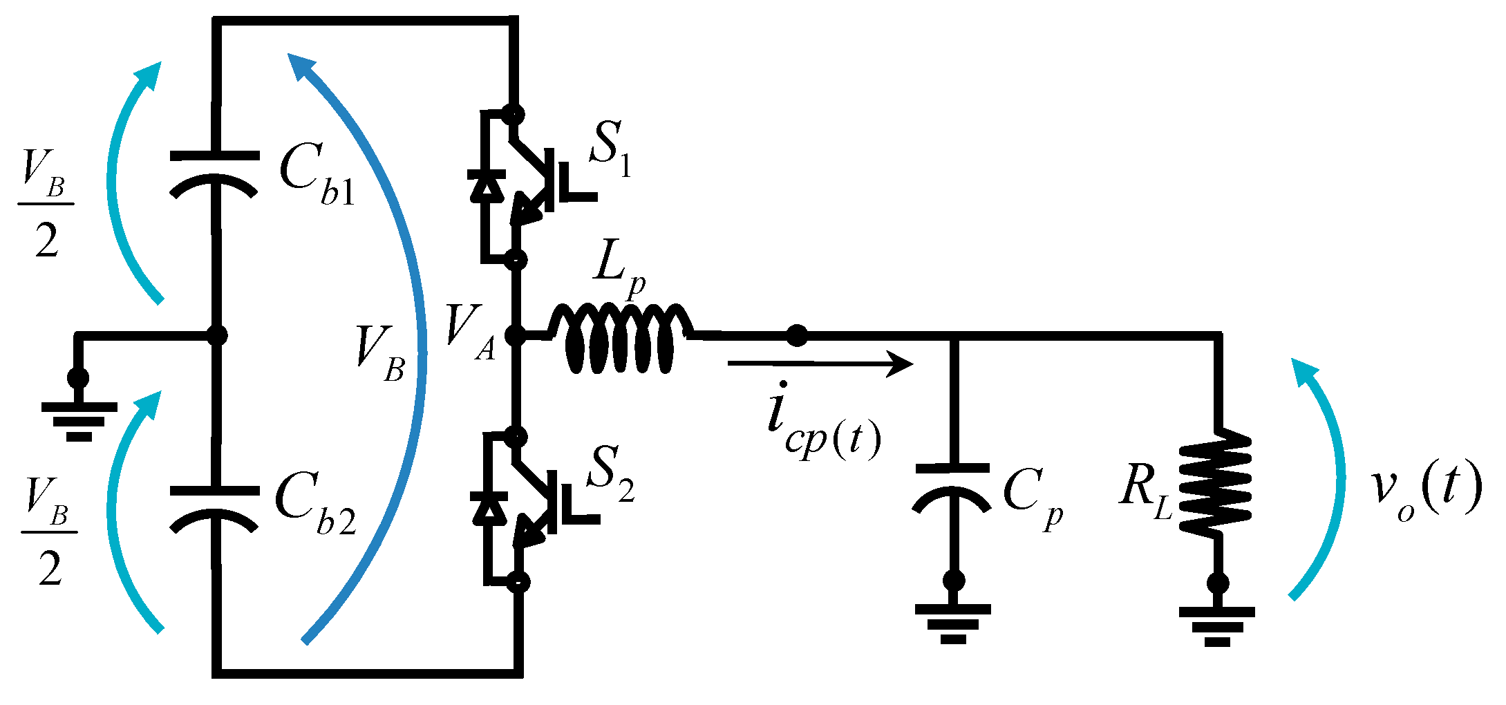
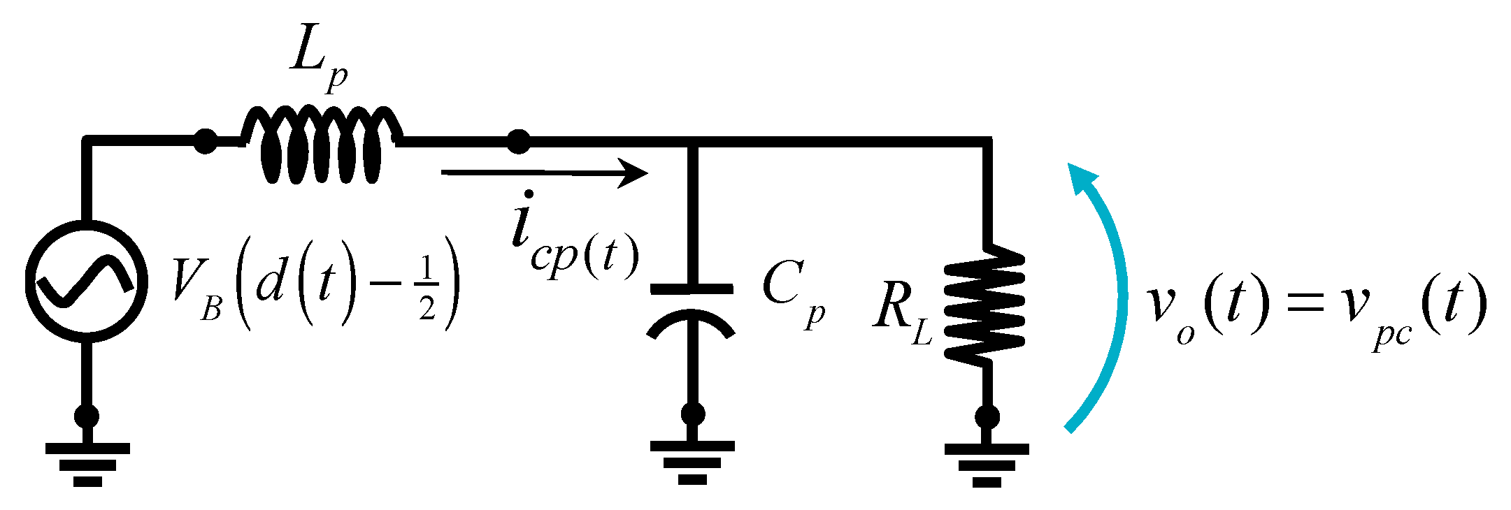
2.2. Shunt Active Power Filter (Shunt APF)

The shunt APF of the dual UPQC aims to provide the load with a sinusoidal voltage of low harmonic distortion and maintain the balance on the three-phase system. The APF consists of a bi-directional power electronics inverter to which a capacitor must be added in parallel to the output.
The transfer function of the shunt APF relates the output voltage with the duty cycle (see Figure 10). Additionally to the parameters defined previously for Figure 1 and Figure 4, the term V o a , V o b , and V o c are the voltage in the load of the power grid; i f s a , i f s b , and i f s c are the filtered currents supplied to the load using the series APF; C p a , C p b , and C p c are the capacitors of the shunt APF; Q 1 - Q 6 are the duty cycle for three-phase inverter; and v r e f is a voltage reference for the voltage controller.
The shunt inverter can be modeled as a single-phase equivalent by the split capacitor characteristic on the DC bus. The circuit in Figure 11 illustrates the equivalent circuit for voltage plant analysis.
From the circuit presented in Figure 11, an equivalent circuit can be obtained as shown in Figure 12, for which the transfer function is given by Equation (20).
G p ( s ) = V o ( s ) D ( s )   = V B L p C p 1 s 2 + ( 1 C p R L ) s + 1 L p C p .

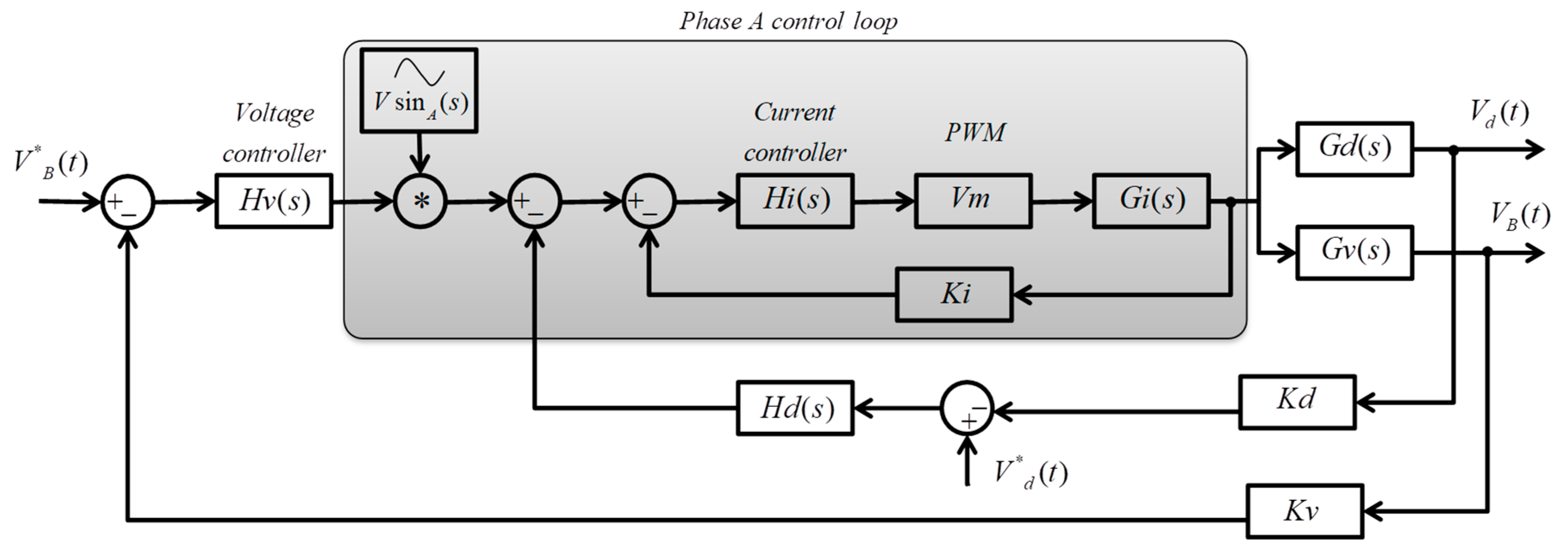
3. Design of Controllers

From the extracted models, the transfer functions for the control can be projected. The controllers will be projected by the method of frequency response for each of the loops of the plant. In order to project controllers, it is necessary to know the frequency response of the system without a controller. Afterward, the frequency and gain requirements of each control actions are determined from the responses. When the transfer function of the controller has been projected, then it is discretized.

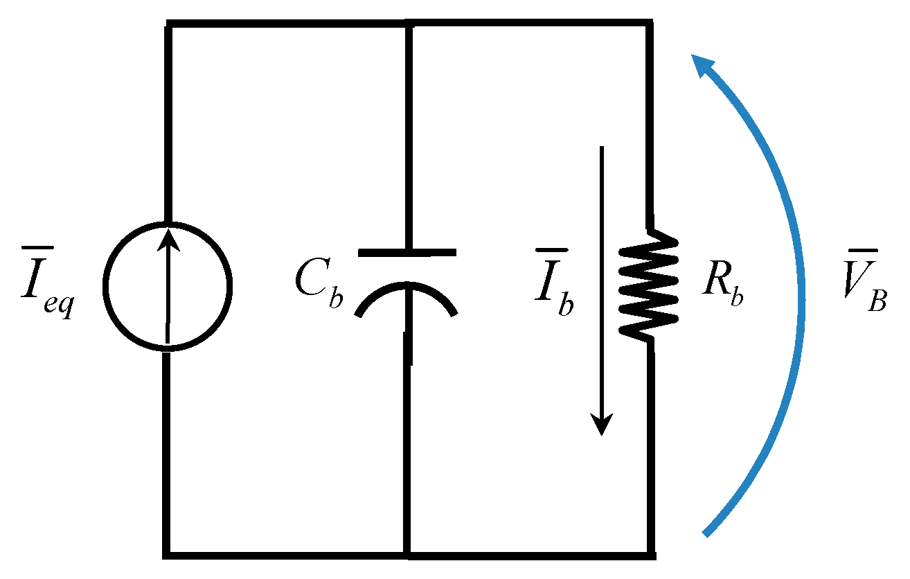
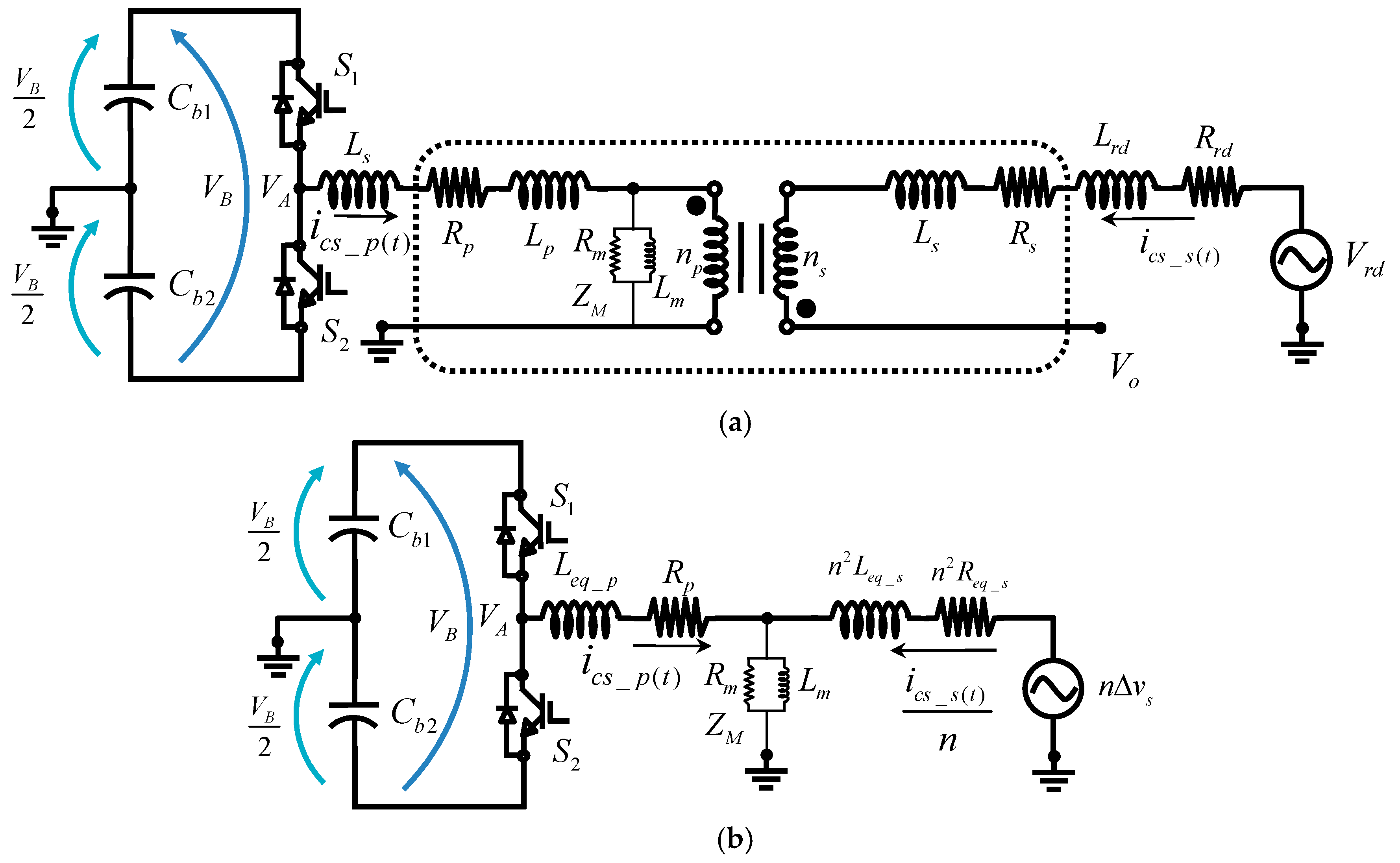
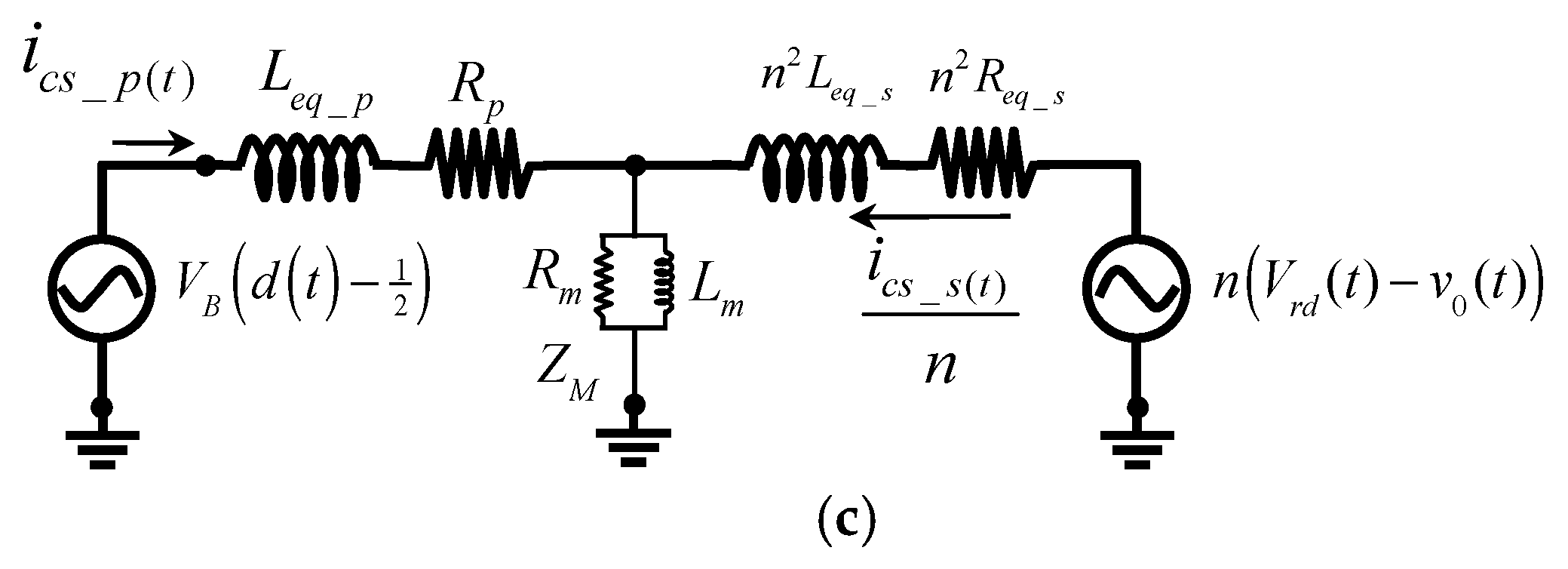
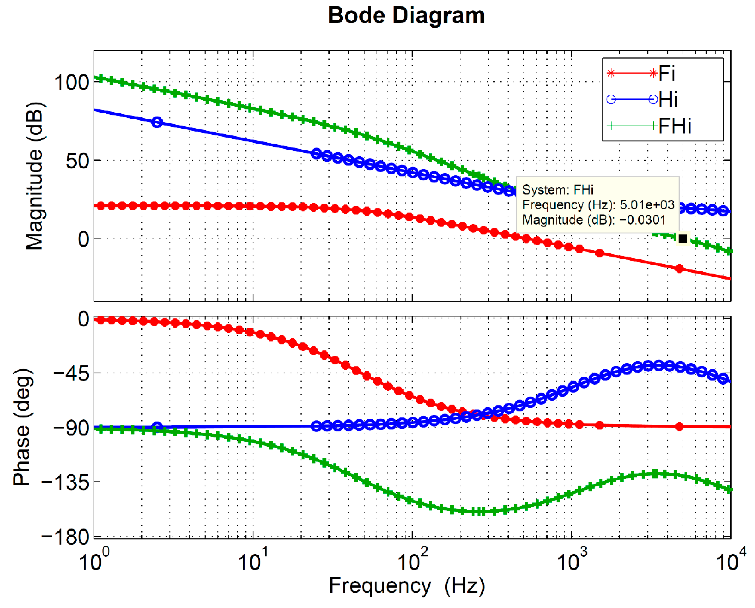
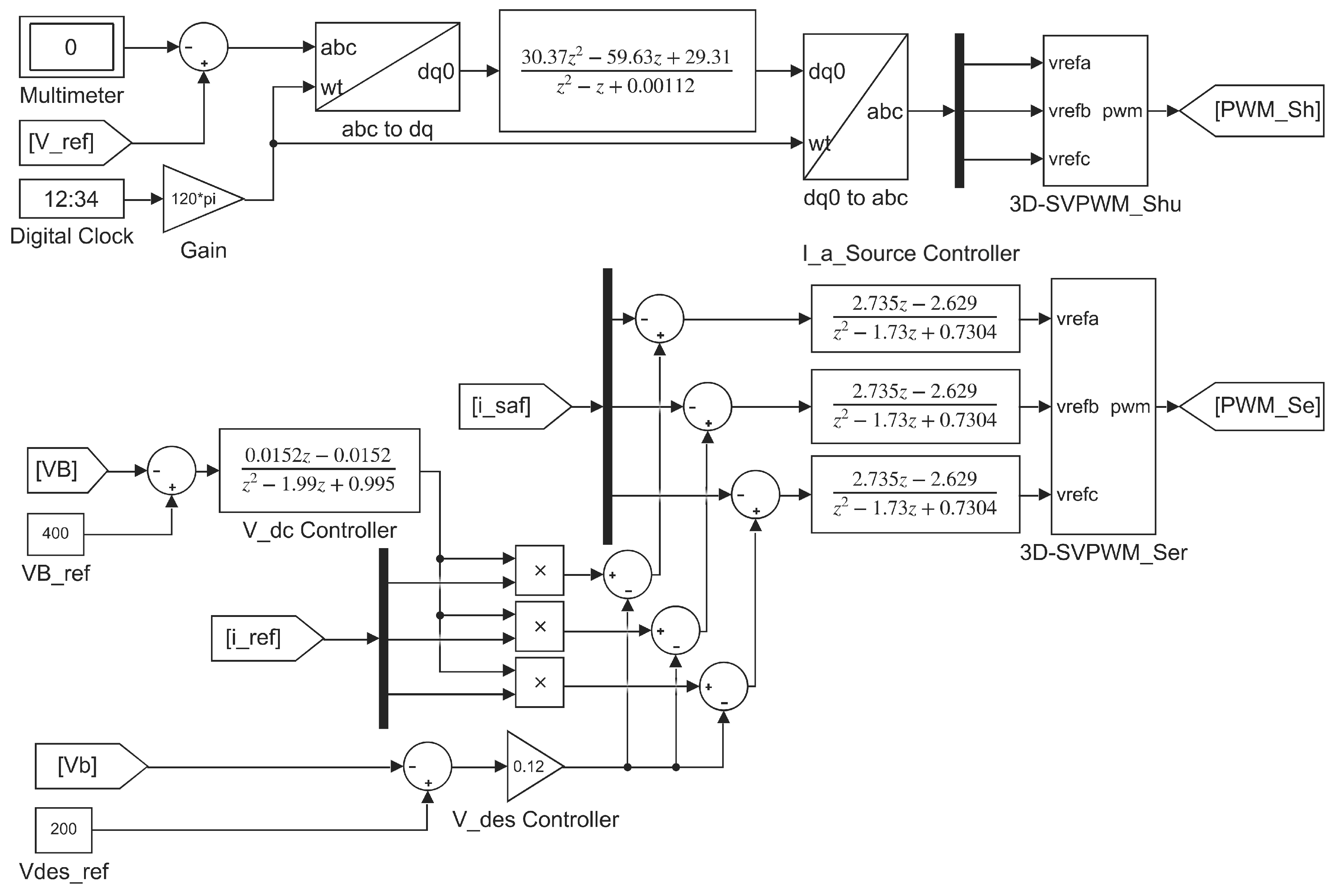
3.1. Current, DC bus, and DC bus Unbalance Controllers

The current controller of the series APF is given by Equation (21), using zero-order hold technique on the input; where the term H i represents the current sensor gain.
H i ( z ) = 2.735 z 2.629 z 2 1.73 z + 0.73 .
Starting from the proportional action, the controller will raise the zero-cross frequency of the system to the required 5 kHz (one-quarter of the switching frequency); the integral action reduces the error in the system and also improves the rejection of disturbances. However, the speed of response is reduced with respect to the proportional action. A pole is added to the PI controller to reduce high-frequency noise. The bode diagram in Figure 13 presents the result of applying the controller to the system.
The DC bus controller and DC bus unbalance controllers are described in Equations (22) and (23); where H D C is the transfer function of the DC bus controller and H u n b is the transfer function of the DC bus unbalance controller.
H D C ( z ) = 15.2 10 3 z 15.2 10 3 z 2 1.99 z + 0.995
H u n b ( z ) = 0.12 .
The DC bus voltage unbalance control is a proportional gain chosen from the maximum current value required to compensate unbalances during transient events, starting from the maximum time in which it must be compensated.

3.2. Voltage Controller

The control strategy selected for the shunt APF consists of PID actions with two poles and two zeros. One of the poles is placed at the source to reduce the speed error and improve noise rejection, the second is positioned at a higher frequency to attenuate high-frequency noise. On the other hand, the zeros are positioned at the same frequency of the poles of the power plant to reduce their effects. The discretized transfer function of the voltage controller in the shunt APF ( H v ) is given by Equation (24).
H v ( z ) = 30.37 z 2 59.63 z + 29.31 z 2 z + 1.12 10 3 .

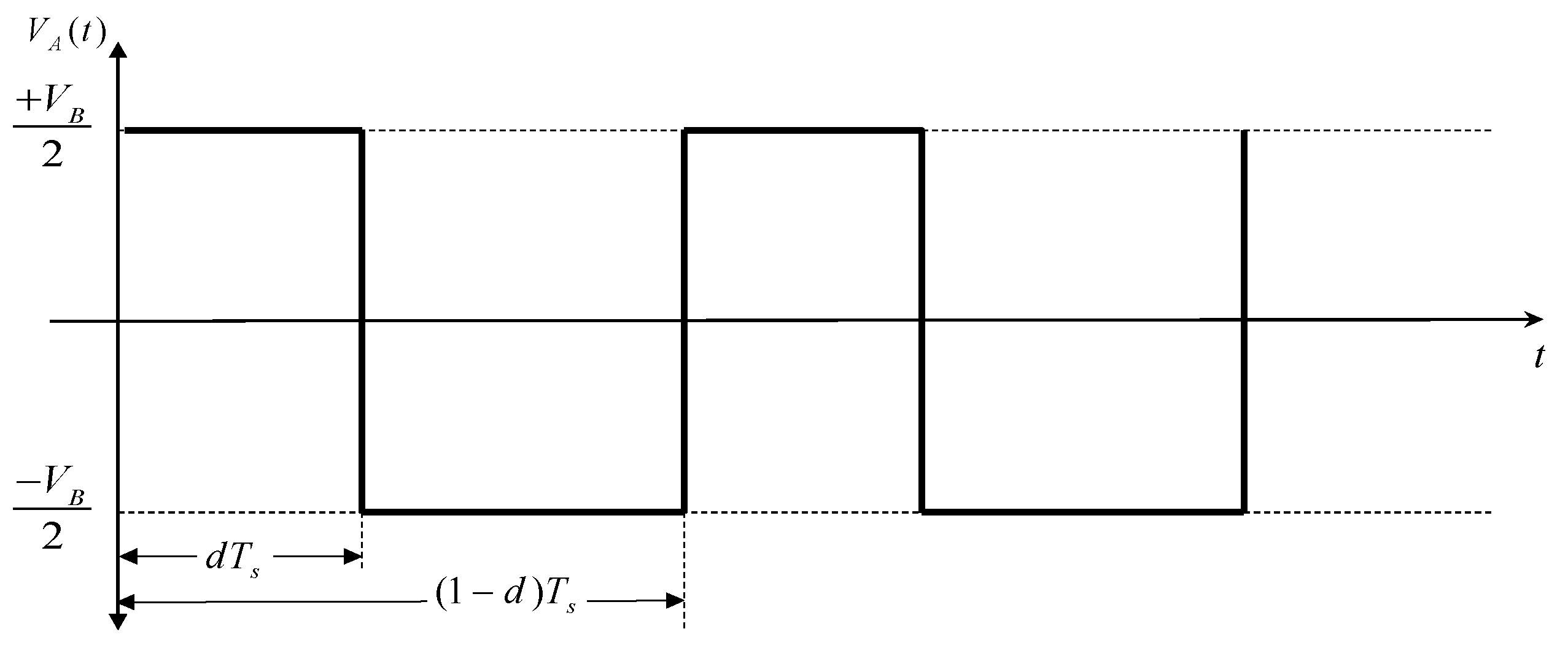
3.3. Three Dimensional Space Vector Pulse Width Modulation (3D-SVPWM)
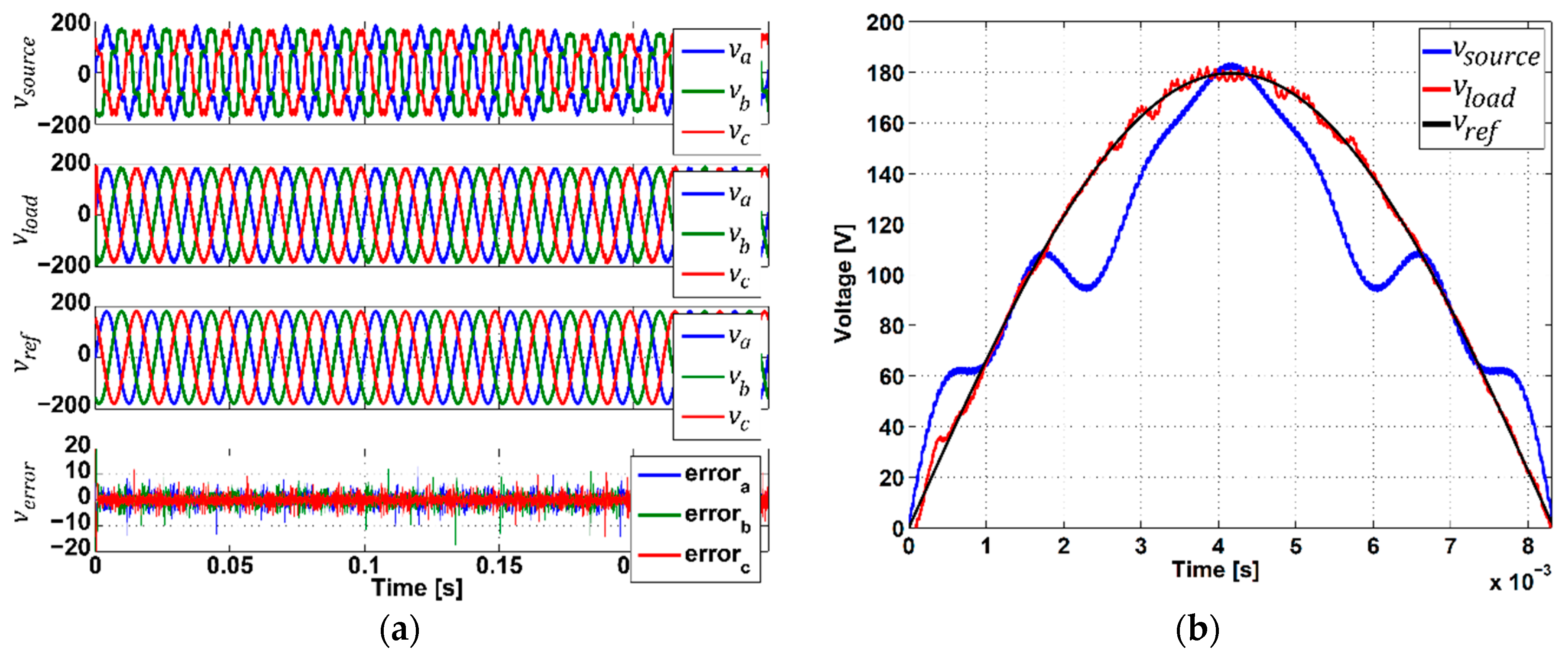
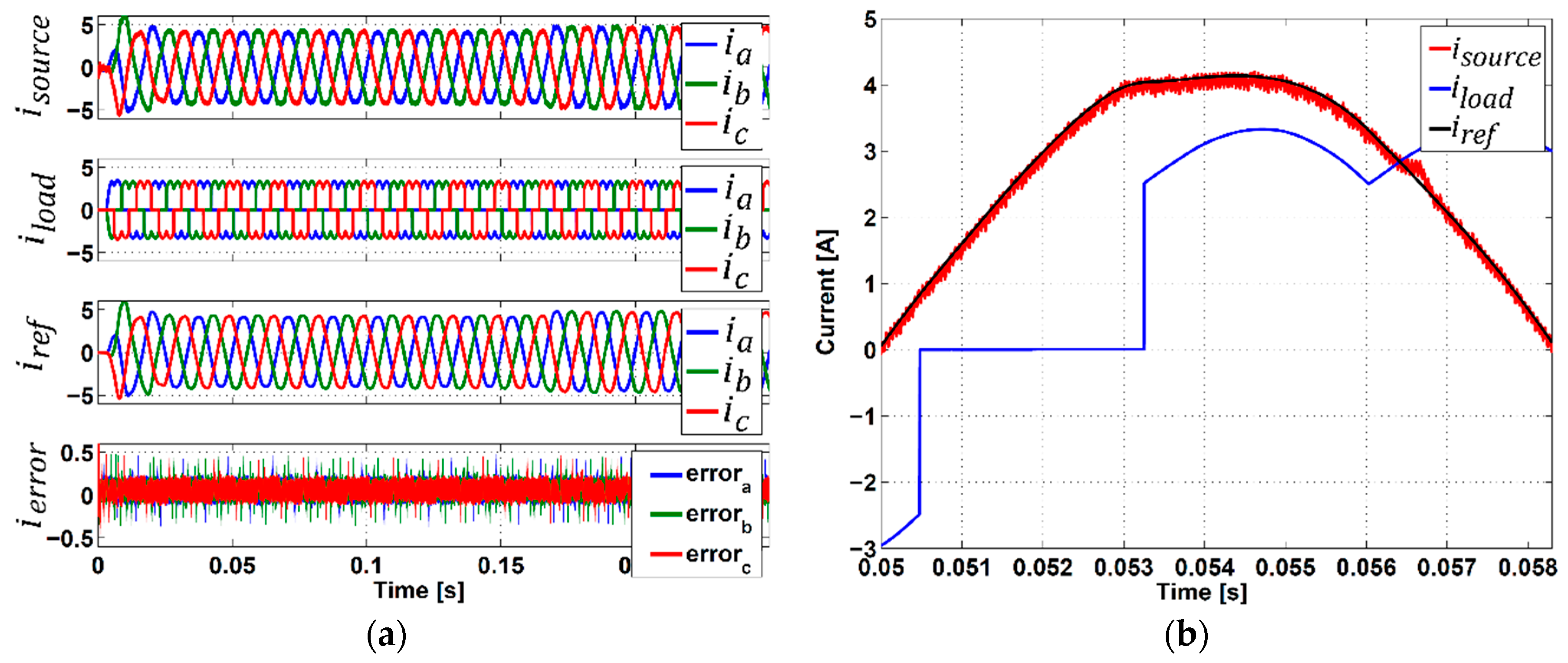
This work proposes the application of a vector modulator for a three-phase split capacitor inverter called three-dimensional three-branch space vector pulse width modulation (3D-3B-SVPWM) [35]. This algorithm has been applied to three-phase inverters switched in parallel connection to compensate current. However, SVPWM modulation is a technique for sinusoidal references; in the case of shunt current compensators, the reference to be generated by the inverter is highly distorted, so the results obtained from the application of this technique do not make sense to give similar results to the SPWM sinusoidal modulation.
The simulation scheme of the controllers is illustrated in Figure 14. In the case of the current controller, the voltage error has been converted to the synchronous reference frame. This transformation allows the use of a single controller for the three phases in the power grid, controlling only the phase components, because the quadrature and zero components are null.

4. Results

The parameters of the transformers, compensators, and the network are given in Table 1. Some of these terms were defined for equations and figures used in Section 1 and Section 2 as parameters per phase of the circuit (a, b, and c); however, in this table those parameters and values are given per phase, omitting the letters. The power is supplied by a 110 VRMS three-phase source that is set unbalanced and contaminated by harmonics. Besides, at a certain time during the simulation, a voltage drop of 10% is generated in the three phases of the power source to verify the behavior of the compensator under this type of transient event. The load considered four AC-DC converters, three full-wave rectifiers to generate unbalances in the load, and a full-wave rectifier controlled by six thyristors to handle delays in the current.
Figure 15a shows the voltage with harmonic distortion in the source, the voltage improved in the load, the voltage reference, and the voltage error of the circuit with the proposed solution. Figure 15b shows the enlargement of the waves referred to the voltages measured in the source and in the load, compared to the voltage reference.
A frequency analysis of the voltage waveforms measured in the source and in the load illustrates the improvement in the harmonic distortion index THDv (in percentage) after the action of the voltage compensator. These results show that the value changes from 14.97% to 1.43%, when applying the compensation, demonstrating the effectiveness of the method. When observing the enlargement of the waves, where an approach has been made to one of the positive half-cycles, the results show that the error between the voltage in the load and the voltage reference is very small, thus achieving a good performance of the compensator. The small ripple in the waveform of the voltage in the load ( V L o a d ) is given by the commutation of the inverters.
Figure 16a shows the current in the source and in the load, the current reference, and the current error. This figure shows that the current in the load is highly contaminated by harmonics and with a delay of 30° with respect to the current in the source, thus acting as a non-linear inductive load. The error between the current in the source and the current reference is less than 5% except for small peaks due to the switching frequency. The detail of the current compensation is better appreciated in the waveforms of Figure 16b, where a mid-period approach of the waves has been made. It can be seen that the total harmonic distortion in current (THDi) goes from a value of 30.94% to 3.37% taking into account the switching frequency of 20 kHz; and if only the harmonic 50 (3 kHz) is considered, the value of THDi = 2.50%, which is half of the maximum value recommended by the IEEE 519 standard.
At 0.01 s, the current of the source presents a transient behavior when the UPQC is connected, due to the requirements of the capacitor in the DC bus to reach its reference voltage. Besides, in Figure 15a a voltage sag has been generated from the source at 0.17 s in order to verify the performance of the UPQC to compensate for the voltage drop. Finally, Figure 16 shows that at the same time the UPQC requires more current from the power source.

5. Conclusions

The continuous model of the UPQC was developed and the classic discrete control model was applied in a three-phase power grid with harmonic distortion and unbalance in the power source. The load of the system was composed of a power electronic AC/DC inverter with phase control to generate current harmonic distortion and low power factor by displacement. The results showed that the series and shunt APFs worked to give good efficiency in filtering the voltage harmonics of the source and the currents harmonics of the load, and to improve the power factor. There is a high-frequency signal in the compensated signals that is due to the switching of the power elements of the UPQC, due to its magnitude; the high-frequency component does not represent a problem for the system and that ends up being filtered by the impedance of the power grid.

Author Contributions

Conceptualization, investigation, methodology, and software, Y.A.G.-G., formal analysis, writing—review, and editing, Y.A.G.-G., J.E.C.-B., and F.E.H.

Funding

This research received no external funding.

Acknowledgments

This work was supported by Universidad Católica de Manizales (Academic Training Unit in Natural Sciences and Mathematics) with the Research Group on Technological and Environmental Developments GIDTA and the Universidad Nacional de Colombia-Sede Medellín, under the projects HERMES-34671 and HERMES-36911. The authors thank the School of Physics and the Department of Electrical Energy and Automation of the Universidad Nacional de Colombia for the valuable help to conduct this research.

Conflicts of Interest

The authors declare no conflict of interest.

References

  1. Gyugyi, L. Unified power-flow control concept for flexible AC transmission systems. IEE Proc. C Gener. Transm. Distrib. 1992, 139, 323–331. [Google Scholar] [CrossRef]
  2. Hingoranl, N.G.; Gyugyi, L.; El-Hawary, M.E. Understanding FACTS: Concepts and Technology of Flexible AC Transmission Systems; Wiley-IEEE Press: Hoboken, NJ, USA, 1999; ISBN 9780470546802. [Google Scholar]
  3. Ghosh, A.; Ledwich, G. Power Quality Enhancement Using Custom Power Devices; Springer: New York, NY, USA, 2002; ISBN 9781461354185. [Google Scholar]
  4. Hingorani, N.G. Introducing custom power. IEEE Spectr. 1995, 32, 41–48. [Google Scholar] [CrossRef]
  5. Khadkikar, V. Enhancing Electric Power Quality Using UPQC: A Comprehensive Overview. IEEE Trans. Power Electron. 2012, 27, 2284–2297. [Google Scholar] [CrossRef]
  6. Mokhtarpour, A.; Shayanfar, H.; Bathaee, S.M.T. Reference Generation of Custom Power Devices (CPs). In An Update on Power Quality; IntechOpen: London, UK, 2013. [Google Scholar]
  7. Taher, S.A.; Afsari, S.A. Optimal location and sizing of UPQC in distribution networks using differential evolution algorithm. Math. Probl. Eng. 2012, 2012. [Google Scholar] [CrossRef]
  8. Dharmalingam, R.; Dash, S.S.; Senthilnathan, K.; Mayilvaganan, A.B.; Chinnamuthu, S. Power quality improvement by unified power quality conditioner based on CSC topology using synchronous reference frame theory. Sci. World J. 2014, 2014, 391975. [Google Scholar] [CrossRef] [PubMed]
  9. Mishra, P.; Kumar Pradhan, A.; Bajpai, P. Voltage control of PV inverter connected to unbalanced distribution system. Renew. Power Gener. IET 2019, 13, 1587–1594. [Google Scholar] [CrossRef]
  10. Hossain, E.; Rida Tür, M.; Padmanaban, S.; Ay, S.; Khan, I. Analysis and Mitigation of Power Quality Issues in Distributed Generation Systems Using Custom Power Devices. IEEE Access 2018, 6, 16816–16833. [Google Scholar] [CrossRef]
  11. Lakshmi, S.; Ganguly, S. An On-line Operational Optimization Approach for Open Unified Power Quality Conditioner for Energy Loss Minimization of Distribution Networks. IEEE Trans. Power Syst. 2019, 34, 4784–4795. [Google Scholar] [CrossRef]
  12. Cheung, V.S.P.; Yeung, R.S.C.; Chung, H.S.H.; Lo, A.W.L.; Wu, W.M. A Transformer-Less Unified Power Quality Conditioner with Fast Dynamic Control. IEEE Trans. Power Electron. 2018, 33, 3926–3937. [Google Scholar] [CrossRef]
  13. Kassai, M.; Poleczky, L.; Al-Hyari, L.; Kajtar, L.; Nyers, J. Investigation of the Energy Recovery Potentials in Ventilation Systems in Different Climates. Facta Univ. Ser. Mech. Eng. 2018, 16, 203–217. [Google Scholar] [CrossRef]
  14. Han, Y.; Xu, L. A survey of the Smart Grid Technologies: background, motivation and practical applications. Prezglad Elektrotechniczky 2011, 87, 47–57. [Google Scholar]
  15. Kassai, M.; Ge, G.; Simonson, C.J. Dehumidification performance investigation of run-around membrane energy exchanger system. Therm. Sci. 2016, 20, 1927–1938. [Google Scholar] [CrossRef]
  16. Garcés Gomez, Y.A.; Toro García, N.; Hoyos, F.E. New Application’s Approach to Unified Power Quality Conditioners for Mitigation of Surge Voltages. J. Electr. Comput. Eng. 2016, 2016. [Google Scholar] [CrossRef]
  17. Monteiro, L.; Exposto, B.; Pinto, G.; Monteiro, V.; Aredes, M.; João, L. Afonso Experimental Evaluation of a Control System Based on a Dual-DSP Architecture for a Unified Power Quality Conditioner. Energies 2019, 12, 1964. [Google Scholar] [CrossRef]
  18. Vigneysh, T.; Kumarappan, N. Grid Interconnection of Renewable Energy Sources Using Unified Power Quality Conditioner: A Fuzzy Logic-Based Approach. J. Circuits, Syst. Comput. 2019, 28, 1959135. [Google Scholar] [CrossRef]
  19. Aredes, M.; Fernandes, R.M. A unified power quality conditioner with voltage SAG/SWELL compensation capability. In Proceedings of the IEEE 2009 Brazilian Power Electronics Conference, Bonito-Mato Grosso do Sul, Brazil, 27 September–1 October 2009; pp. 218–224. [Google Scholar]
  20. França, B.W.; Aredes, M. Comparisons between the UPQC and its dual topology (iUPQC) in dynamic response and steady-state. In Proceedings of the IECON 2011—37th Annual Conference of the IEEE Industrial Electronics Society, Melbourne, Australia, 7–10 November 2011; IEEE: Piscataway, NJ, USA, 2012; pp. 1232–1237. [Google Scholar]
  21. Millnitz dos Santos, R.J.; Mezaroba, M.; da Cunha, J.C. A Dual Unified Power Quality Conditioner Using a Simplified Control Technique. In Proceedings of the IEEE XI Brazilian Power Electronics Conference, Praiamar, Brazil, 11–15 September 2011; IEEE: Piscataway, NJ, USA, 2011; pp. 486–493. [Google Scholar]
  22. Wang, J.; Wu, H.; Sun, K.; Zhang, L. A High Efficiency Quasi-Single-Stage Unified Power Quality Conditioner Integrating Distributed Generation. In Proceedings of the 2019 IEEE 10th International Symposium on Power Electronics for Distributed Generation Systems (PEDG), Xi’an, China, 3–6 June 2019; IEEE: Piscataway, NJ, USA, 2019. [Google Scholar]
  23. Oliveira da Silva, S.A.; Garcia Campanhol, L.B.; de Souza, V. Dynamic Performance Evaluation of a dual UPQC Operating Under Power Quality Disturbances. In Proceedings of the PCIM Europe 2018; International Exhibition and Conference for Power Electronics, Intelligent Motion, Renewable Energy and Energy Management, Nuremberg, Germany, 5–7 June 2018; IEEE: Piscataway, NJ, USA, 2018. [Google Scholar]
  24. Modesto, R.A.; Oliveira da Silva, S.A.; de Oliveira Júnior, A.A. Power quality improvement using a dual unified power quality conditioner/uninterruptible power supply in three-phase four-wire systems. IET Power Electron. 2015, 8, 1595–1605. [Google Scholar] [CrossRef]
  25. Transformerless Series Active Power Filter to Compensate Voltage Disturbances—IEEE Conference Publication. Available online: https://ieeexplore.ieee.org/document/6020368 (accessed on 7 November 2019).
  26. Banaei, M.R.; Hosseini, S.H. Mitigation of Current Harmonic Using Adaptive Neural Network with Active Power Line Conditioner. In Proceedings of the 2006 CES/IEEE 5th International Power Electronics and Motion Control Conference, Shanghai, China, 14–16 August 2006; IEEE: Piscataway, NJ, USA, 2009; pp. 1–5. [Google Scholar]
  27. Ming, Z.; Jian-Ru, W.; Zhi-Qiang, W.; Jian, C. Control Method for Power Quality Compensation Based on Levenberg-Marquardt Optimized BP Neural Networks. In Proceedings of the 2006 CES/IEEE 5th International Power Electronics and Motion Control Conference, Shanghai, China, 14–16 August 2006; IEEE: Piscataway, NJ, USA, 2009; pp. 1–4. [Google Scholar]
  28. Forghani, M.; Afsharnia, S. Online Wavelet Transform-Based Control Strategy for UPQC Control System. IEEE Trans. Power Deliv. 2007, 22, 481–491. [Google Scholar] [CrossRef]
  29. Karthikeyan, N.; Mishra, M.K.; Kalyan Kumar, B. Complex wavelet based control strategy for UPQC. In Proceedings of the 2010 Joint International Conference on Power Electronics, Drives and Energy Systems & 2010 Power India, New Delhi, India, 20–23 December 2010; IEEE: Piscataway, NJ, USA, 2011; pp. 1–6. [Google Scholar]
  30. Kesler, M.; Ozdemir, E. A novel control method for unified power quality conditioner (UPQC) under non-ideal mains voltage and unbalanced load conditions. In Proceedings of the 2010 Twenty-Fifth Annual IEEE Applied Power Electronics Conference and Exposition (APEC), Palm Springs, CA, USA, 21–25 Febrary 2010; IEEE: Piscataway, NJ, USA, 2010; pp. 374–379. [Google Scholar]
  31. Lee, W.C.; Lee, D.M.; Lee, T.K. New Control Scheme for a Unified Power-Quality Compensator-Q With Minimum Active Power Injection. IEEE Trans. Power Deliv. 2010, 25, 1068–1076. [Google Scholar] [CrossRef]
  32. Hoyos Velasco, F.E.; Toro-García, N.; Garcés Gómez, Y.A. Adaptive Control for Buck Power Converter Using Fixed Point Inducting Control and Zero Average Dynamics Strategies. Int. J. Bifurc. Chaos 2015, 25, 1550049. [Google Scholar] [CrossRef]
  33. Mohan, N. Power Electronics: A First Course; Wiley: Hoboken, NJ, USA, 2011. [Google Scholar]
  34. Mohan, N.; Undeland, T.M.; Robbins, W.P. Power Electronics: Converters, Applications and Design, 3rd ed.; John Wiley & Sons: New York, NY, USA, 2002. [Google Scholar]
  35. Orts, S.; Sales, F.G.; Chilet, S.S.; Alcaniz, M.; Masot, R.; Abellan, A. New active compensator based on ieee std. 1459. IEEE Lat. Am. Trans. 2006, 4, 38–46. [Google Scholar] [CrossRef]
Figure 1. Diagram of power quality unified conditioner (UPQC).
Applsci 09 05087 g001
Figure 2. UPQC in traditional topology.
Applsci 09 05087 g002
Figure 3. UPQC in dual topology.
Applsci 09 05087 g003
Figure 4. Series active power filter (series APF) for the UPQC in dual topology.
Applsci 09 05087 g004
Figure 5. Series APF diagram.
Applsci 09 05087 g005
Figure 6. Circuit to model the series APF in the UPQC, (a) single-phase circuit, (b) circuit referred to the primary of the transformer, and (c) equivalent circuit.
Applsci 09 05087 g006aApplsci 09 05087 g006b
Figure 7. Representation of the switching period.
Applsci 09 05087 g007
Figure 8. Equivalent circuit of the DC bus.
Applsci 09 05087 g008
Figure 9. Equivalent circuit of the current loop.
Applsci 09 05087 g009
Figure 10. Shunt active power filter (shunt APF) for the UPQC in dual topology.
Applsci 09 05087 g010
Figure 11. Single-phase circuit of the shunt APF.
Applsci 09 05087 g011
Figure 12. Shunt active power filter single-phase equivalent circuit.
Applsci 09 05087 g012
Figure 13. Frequency response in the current loop with and without the controller.
Applsci 09 05087 g013
Figure 14. Controllers simulation scheme.
Applsci 09 05087 g014
Figure 15. Voltage compensation results: (a) three-phase signals and (b) zoom of the waveform.
Applsci 09 05087 g015
Figure 16. Current compensation results: (a) three-phase signals and (b) zoom of the waveform.
Applsci 09 05087 g016
Table 1. Parameters of the transformers, compensators, and the network.
NameParameterValue
Inductance of the series APF L s 650 μH
Switching frequency F s 20 kHz
DC link voltage V B 400 V
PWM voltage gain V m 0.091 V
Power grid resistance R r d 0.04 Ω
Power grid inductance L r d 107 μH
Power grid capacitance C s 1 μF
Shunt inductance L p 1.2 mH
Shunt and series resistance R p   =   R s 0.44 Ω
Magnetizing resistance of the transformer R m 104 Ω
Magnetizing inductance of the transformer L m 104 H
Secondary equivalent resistance R e q _ s 0.48 Ω
DC bus total capacitance C B 3 mF
Secondary equivalent inductance L e q _ s 757 μH
Primary equivalent inductance L e q _ p 1.85 mH

