Article

Design and Implementation of a System-on-Chip for Self-Calibration of an Angular Position Sensor

1
Engineering Research Center for Navigation Technology, Department of Precision Instrument, Tsinghua University, Beijing 100084, China
2
Department of Mechanical Engineering, Tsinghua University, Beijing 100084, China
*
Authors to whom correspondence should be addressed.
Appl. Sci. 2019, 9(22), 4772; https://doi.org/10.3390/app9224772
Submission received: 10 October 2019 / Revised: 6 November 2019 / Accepted: 6 November 2019 / Published: 8 November 2019
(This article belongs to the Special Issue Implementation of Vehicular Cloud Networks Using Wireless Sensor)

Abstract

:

Featured Application

The designed hardware is low cost and easy to implement. It can simplify the complexity of the sensor calibration process and can be free of high-precision but expensive calibration equipment.

Abstract

In this study, a novel signal processing algorithm and hardware processing circuit for the self-calibration of angular position sensors is proposed. To calibrate error components commonly found in angular position sensors, a parameter identification algorithm based on the least mean square error demodulation is developed. A processor to run programs and a coprocessor based on the above algorithm are used and designed to form a System-on-Chip, which can calibrate signals as well as implement parameter configuration and control algorithm applications. In order to verify the theoretical validity of the design, analysis and simulation verification of the scheme are carried out, and the maximum absolute error value in the algorithm simulation is reduced to 0.003 %. The circuit’s Register-Transfer Level simulation shows that the maximum absolute value of the angular error is reduced to 0.03%. Simulation results verify the calibration performance with and without quantization and rounding error, respectively. The entire system is prototyped on a Field Programmable Gate Array and tested on a Capacitive Angular Position Sensor. The proposed scheme can reduce the absolute value of angular error to 4.36%, compared to 7.68% from the experimental results of a different calibration scheme.

1. Introduction

In some mechatronic systems, acquiring angle information is a prerequisite for implementing control strategies or performing information processing [1]. Resolvers [2] and Capacitive Angular Position Sensors (CAPS) can be used for angle acquisition [3]. These sensors detect angle information and output two related orthogonal sine and cosine signals through signal modulation and demodulation.
In practical applications, output signals usually contain amplitude deviations, direct-current (DC) offsets, and a phase shift [3]. The output signals can be described by Equation (1):
  U = a 1 sin θ + b 1 , V = a 2 cos ( θ + β ) + b 2 .
To improve sensor accuracy, error components need to be identified and the sine and cosine signals should be extracted according to the identification results. Parameter identification based on input and output signals [4,5] of the sensor is an effective solution. In applications where the input signal is not directly available, self-calibration schemes are more widely applicable. Self-calibration based on a least mean square algorithm was first proposed in [6]. According to this scheme, an ellipse fitting method [7] and a parameter identification algorithm [1,8] based on gradient descent were developed. On this basis, Gao [9,10] proposed iterative algorithms for self-calibration, while Wu et al. [11] applied the technology detailed in [12] to design a two-step gradient estimator and realize online parameter self-calibration.
Self-calibration in hardware eliminates the need for additional offline data processing, further simplifying the sensor calibration process. Hung et al. [13] designed a code compensator to extract position information for magnetic encoders. Hieu et al. [14] proposed an interpolation technique to improve position information accuracy. These methods were more concerned with suppressing error sources. For the processing of error signals, Hyun et al. [15] proposed an adaptive digital demodulation method for a sinusoidal encoder signal, and Xiujun et al. [16] developed a piecewise calibration technique that provided a good trade-off between microcontroller memory size and algorithm complexity. The scheme in [11] was also a self-calibration method implemented in hardware. Simpler signal processing algorithms generally consume fewer hardware resources, motivating the solution proposed in this study.
This paper applies a Least Mean Square Error Demodulation (LMSED) algorithm for parameter identification and self-calibration. This algorithm uses simple mathematical operations and a coprocessor based on the algorithm is designed to handle the entire self-calibration process, including parameter identification and angle calculation. A System-on-Chip (SoC) with the coprocessor is also designed to implement parameter configuration and further signal processing. The SoC core is Arm Cortex-M3 [17], which is the industry-leading 32-bit low power processor for highly deterministic real-time applications. The coprocessor communicates with the core through Advanced Peripheral Bus (APB) for data and control information. The prototype verification is performed on a Field Programmable Gate Array (FPGA) development board, and the FPGA is used for self-calibration of the CAPS.
This paper is organized as follows. Section 2 discusses the signal model and issues that need to be resolved. Section 3 presents the architecture of the SoC, as well as the theoretical analysis and implementation details of the coprocessor are presented. Section 4 details the algorithm simulation, Register-Transfer Level (RTL) simulation for the coprocessor, FGPA experiments, and the CAPS. Finally, Section 5 provides conclusions and future research plans.

2. Problem Description

The working principle of the CAPS used in the experiment is shown in Figure 1:
Under the influence of excitation voltage [3], the sensor outputs two signals ( U 0 and V 0 ), which can be expressed as Equation (2):
  U 0 = k E cos ( ω 0 t ) sin ( θ ) , V 0 = k E cos ( ω 0 t ) cos ( θ ) .
where k is the gain coefficient, ω 0 and E are the frequency and amplitude of the excitation voltage, respectively, and θ is the angle to be measured. Ideally, the output signals after envelop detection follow Equation (3):
  U = sin ( θ ) , V = cos ( θ ) .
With the presence of interference factors, output signals are defined by Equation (1). When the amplitudes of the interference terms are recognized, signal calibration can be performed based on Equation (4):
  U = U f = ( U b ^ 1 ) / a ^ 1 = sin θ , V = V f = ( V b ^ 2 ) / ( a ^ 2 cos β ^ ) + ( U b ^ 1 ) tan β ^ / a ^ 1 = cos θ .
where β is the identified phase shift, a ^ 1 and a ^ 2 are the identified amplitudes, b ^ 1 and b ^ 2 are the identified DC offsets.
Our research objectives include studying the parameter identification algorithm, as well as integrating the parameter identification and angle calculation process into the digital circuit to realize self-calibration in hardware.

3. Calibration Method Design

3.1. Architecture Description of the Proposed SoC

The calibration scheme is implemented in a SoC based on the Cortex-M3 processor. The SoC combines software control and hardware calculation for more flexible processing of signals. As shown in Figure 2, the system collects digital signals from the sensors through an analog to digital converter and calibrates the signals through an on-chip self-calibration module, which is performed in the coprocessor. The coprocessor implements signal demodulation and angle calculation, while the parameter configuration and control algorithm is implemented in the Cortex-M3 processor. The General Purpose Input Output (GPIO) is used for signal output during debugging. The Universal Asynchronous Receiver/Transmitter (UART) is used to send measurement data to the computer for further processing. The Phase Locked Loop (PLL) is used to generate the system clock signal, while the Static Random-Access Memory (SRAM) is used to store the program and data.
Throughout the system architecture, Cortex-M3 is an open source IP processor core for education. As a low-power 32-bit processor, it has been widely used in the embedded field. AHB and APB belong to ARM’s Advanced Microcontroller Bus Architecture (AMBA), which defines the data and command communication between the processor core and external devices. It is an industrial bus protocol. They are designed with combinatorial logic for performing the assignment of data and instructions. Among them, AHB is used for high-speed communication with the processor core, and APB is used for low-speed traffic with peripherals. The self-calibration module is a module designed and proposed, and the mathematical principles and implementations involved are described in the next section. The UART implements communication between the system and other communication devices, and supports baud rate generation, data transmission and reception, and interrupt control. Since the module is mounted on the APB, an additional APB-UART interface module design is required. The PLL is a module that generates a clock that drives the entire system, and mainly includes a phase detector, a loop filter, and a voltage controlled oscillator. The design at the FPGA level can call the IP provided by Altera Corporation. SRAM is used to store programs and data. It can be described and designed with registers and combinatorial logic. It can also call IP generation. In the experiment, IP generation method is adopted for design.
The system has two operation modes: demodulation and calibration. In the demodulation mode, the coprocessor generates sinusoidal, cosine, and DC signals as a set of bases to perform parameter identification of the two sensor output signals. In calibration mode, the coprocessor calibrates the signal based on the parameter values obtained in demodulation mode, and then calculates the angular value measured by the sensor. Demodulation mode operates when the measurement angle signal changes at a certain frequency, while calibration mode does not have this constraint. Both modes allow gating control and the control signal comes from the program running in the Cortex-M3 processor.
The self-calibration coprocessor is designed for signal demodulation and angle calibration, which is the key system module. The demodulation module is based on least mean square error, which is described in the next section.

3.2. Design of Self-Calibration Coprocessor Based on LMSED

The coprocessor is mounted on the low speed APB for real-time data acquisition and processing. It is mainly composed of three modules: parameter identification, signal calibration, and angle calculation. The parameter identification and signal calibration modules form the self-calibration part, whose architecture is shown in Figure 3. The parameter identification module uses the LMSED algorithm to solve the sine, cosine, and DC signal component values. Parameter calculation is then performed based on these values. The LMSED process only occurs in demodulation mode, while calculation mode directly uses the parameter calculation results to calibrate the signals.
Demodulation mode works when the measured signal changes at a certain frequency. In this case, the signal model can be expressed as
  U ( k ) = a 1 sin ( ω c k + φ ) + b 1 , V ( k ) = a 2 cos ( ω c k + φ + β ) + b 2 .
where k is the number of sampling points, ω c is the rotation speed of the angle, and φ is the phase difference between the reference signal and the measured signal. With reference sine, cosine, and DC components, Equation (5) can be expressed as
  U ( k ) = a 1 cos ( φ ) sin ( ω c k ) + a 1 sin ( φ ) cos ( ω c k ) + b 1 , V ( k ) = a 2 sin ( φ + β ) sin ( ω c k ) +   a 2 cos ( φ + β ) cos ( ω c k ) + b 2 .
Equation (6) can then be simplified to
  U ( k ) = a u sin ( ω c k ) + b u cos ( ω c k ) + c u , V ( k ) = a v sin ( ω c k ) +   b v cos ( ω c k ) + c v .
where the relationship between the reference signal components and measured signal parameters can be expressed as
  a u = a 1 cos ( φ ) , b u = a 1 sin ( φ ) , c u = b 1 , a v = a 2 sin ( φ + β ) , b v = a 2 cos ( φ + β ) , c v = b 2 .
The demodulation module obtains the coefficients of Equation (8) based on the LMSED algorithm; the principles and implementation details of this process are described in the next section. The parameter calculation module obtains the parameters of the two signals based on the relationship in Equation (8), and performs numerical calculations as shown in Equation (9):
  a 1 = a u 2 + b u 2 , b 1 = c u , a 2 = a v 2 + b v 2 , b 2 = c v , φ = atan ( b u a u ) , β = atan ( a v b v ) φ .
The root number and arctangent operations are contained in this module. The root number operation is performed in the digital circuit based on the fixed point iteration method [18], and is approximated by 30 iterations. For the problem of y 2 = x , the following iterative calculation method is used:
y k + 1 = y k 2 x + y k , y 0 = 0 .
The design principle of the root number operation module is shown in Equation (10). In the design process, the clock used by the module is 32 times the main drive clock. Among them, the first clock cycle is used to latch the operand, 30 clock cycles are used to complete 30 iteration calculations, and the last clock cycle is used to latch the calculation result and provide an output valid signal.
The arctangent operation is based on a proportional-integral (PI) controller [19], which refers to the working principle of AD2S1210 [20]. The working schematic is shown in Figure 4. The digital controller reduces the error value by adjusting the value of the reference signal. In the ideal case, when the error value is 0, the value of the reference signal is equal to the true angle value. Therefore, the iteratively adjusted reference signal value can be used as the calculated value of the real angle.
The iteration formula is
e r r k = u cos ( φ k ) v sin ( φ k ) , φ 0 = 0 , φ k + 1 = φ k + P ( e r r k e r r k 1 ) + I e r r k .
The calculations for the reference sine and cosine signals use the look-up table and interpolation method to obtain values in one clock cycle [21]. The purpose of the look-up table is to quantify the operands and obtain the exact values at the nodes. Interpolation is to obtain a more accurate output using a linear fitting method. The look-up table uses a ROM for data storage and data access via address lines. The read data is interpolated by multiplication and addition operations, and all designs are implemented by combinatorial logic. The number of iterations is set to 30 in the design. A module clock of 32 times the main drive clock is also used. Among them, the first clock cycle is used to latch the operand, 30 clock cycles are used to complete 30 iteration calculations, and the last clock cycle is used to latch the calculation result and provide an output valid signal.
With the root number and arctangent operations, parameter identification can be performed after the LMSED process. Based on the identified parameter values, the signal calibration module eliminates the phase differences of the two measurement signals and equalizes the amplitudes. The module performs the following numerical operations:
U 1 ( k ) = a 2 ( U ( k ) b 1 ) = a 1 a 2 sin ( ω c k + φ ) , V 1 ( k ) = a 1 ( V ( k ) b 2 ) = a 1 a 2 ( cos ( ω c k + φ ) cos ( β ) sin ( ω c k + φ ) sin ( β ) ) , U 2 ( k ) = U 1 ( k ) cos ( β ) , V 2 ( k ) = V 1 ( k ) + U 1 ( k ) sin ( β ) .
where U 2 ( k ) and V 2 ( k ) are calibrated signals. These signals are fed into the angle calculation module to obtain calibrated angle information. The calculations processed by the calculation module are multiplication and addition and subtraction operations. The design uses two levels of registers to buffer the input operands and the output calculation results. The combination logic is used to complete all operations.

3.3. Theoretical Analysis and Implementation Details of the LMSED Module

The LMSED uses an adaptive algorithm to extract signal amplitude information, which is commonly used in the signal analysis [22,23,24]. This method is simple, does not require complicated mathematical operations, and is easy to implement in digital circuits.
The designed LMSED module processes signals with the following expressions:
d ( k ) = s ( k ) + n ( k ) , s ( k ) = a 1 sin ( ω c k ) + b 1 cos ( ω c k ) + c 1 .
where n ( k ) indicates signal noise, ω c is the signal frequency, and k represents the sampling time. The coefficient vector is used to represent the signal’s DC components, sine and cosine components, and it is iteratively solved during the demodulation process using Equation (14):
W = ( W 1 , W 2 , W 3 ) T , W 1 = a 1 , W 2 = b 1 , W 3 = c 1 .
The vector representation of the reference signals is
r ( k ) = ( sin ( ω c k ) , cos ( ω c k ) , 1 ) T .
The reference sine and cosine signals are generated by a signal generator based on a Cordic algorithm [25], with a bit width of 32 and a pipeline depth of 28, achieving 24-bit precision. The driving frequency of the Cordic calculation module is also 32 times the main clock. The first clock cycle is used to latch the operands, the 28 clock cycles are used to complete the pipeline calculation, the 30th clock cycle is used for quadrant judgment and symbol correction, and the 31st clock cycle is used to obtain the exact signal. In order to reduce the number of drive clocks in the entire system, the clock is used 32 times and data latching continues in the 32nd clock cycle.
The working principle of the LMSED scheme is shown in Figure 5. The component in the prediction matrix W is the parameter to be identified in Equation (7). The reference signal r ( k ) and prediction matrix are used to calculate the inner product and obtain the estimated value of the input signal. The estimated value is compared with the input signal to obtain the error between the estimated and true values. The prediction matrix is adjusted iteratively to minimize the expected value of the squared error.
In the algorithm implementation process, there are two types of error models:
η ( k ) = s ( k ) W T r ( k ) , e r r ( k ) = d ( k ) W T r ( k ) ,
The identification process adjusts parameter values by iteration. The optimization function of the iterative process is min { E [ η 2 ( k ) | W ] } while only the e r r ( k ) can be calculated in the demodulation process. For theoretical analysis, if the noise data follow a normal distribution with a mean of 0 and a variance of σ 2 , Equation (17) is established:
E [ e r r 2 ( k ) | W ] = E [ ( η ( k ) + n ( k ) ) 2 | W ] = E [ η 2 ( k ) | W ] + σ 2 .
Based on Equation (17), the optimization function can also be set to
min { E [ e r r 2 ( k ) | W ] } .
With the optimization function mentioned above, the parameter adjustment rule of the iterative process is performed based on the gradient descent method [26]. To simplify the number of calculations in the iterative process, the squared error is used as the optimization function to replace the expected value of the error. The gradient formula is as follows:
e r r 2 ( k ) W = 2 e r r ( k ) e r r ( k ) W = 2 e r r ( k ) r ( k ) .
Based on Equation (19), the update formula of the parameters is
W ( k + 1 ) = W ( k ) + 2 e r r ( k ) μ r ( k ) .
where μ is the step factor used to adjust the parameters’ update speed. As the iteration progresses, the parameters gradually converge to the true value.
In the implementation process, the operations and operations involved are implemented by combinatorial logic. The operands and some parameters are designed to be read and written by the APB bus. This means that the user can modify the parameter configuration by modifying the algorithm running in the processor.

4. Simulation and Experimental Results

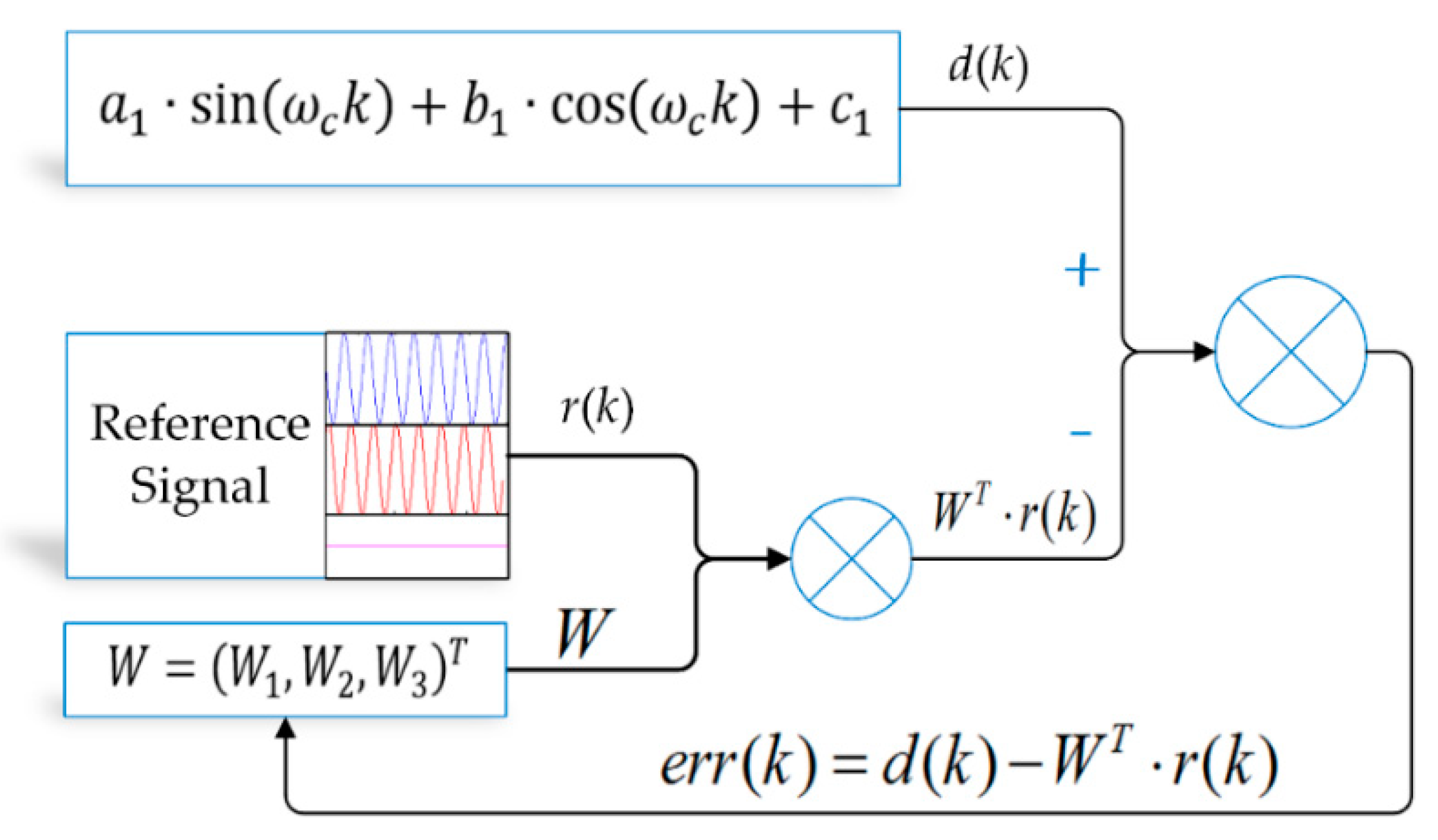
4.1. LMSED Algorithm Simulation

4.1.1. Feasibility Verification and Convergence Speed Analysis

In order to verify the proposed scheme’s feasibility, simulation experiments were performed first. The LMSED algorithm was verified using the MATLAB software platform.
In the simulation, the frequency of the input angle is f c = 0.05 Hz and the sample frequency is 250 Hz. The simulation model used to generate simulation data is based on Equation (21):
U ( k ) = 0.6079 sin ( 2 π f c k + 0.0876 ) + 0.1336 , V ( k ) = 0.6228 cos ( 2 π f c k + 0.0876 + 0.0629 ) + 0.1831 .
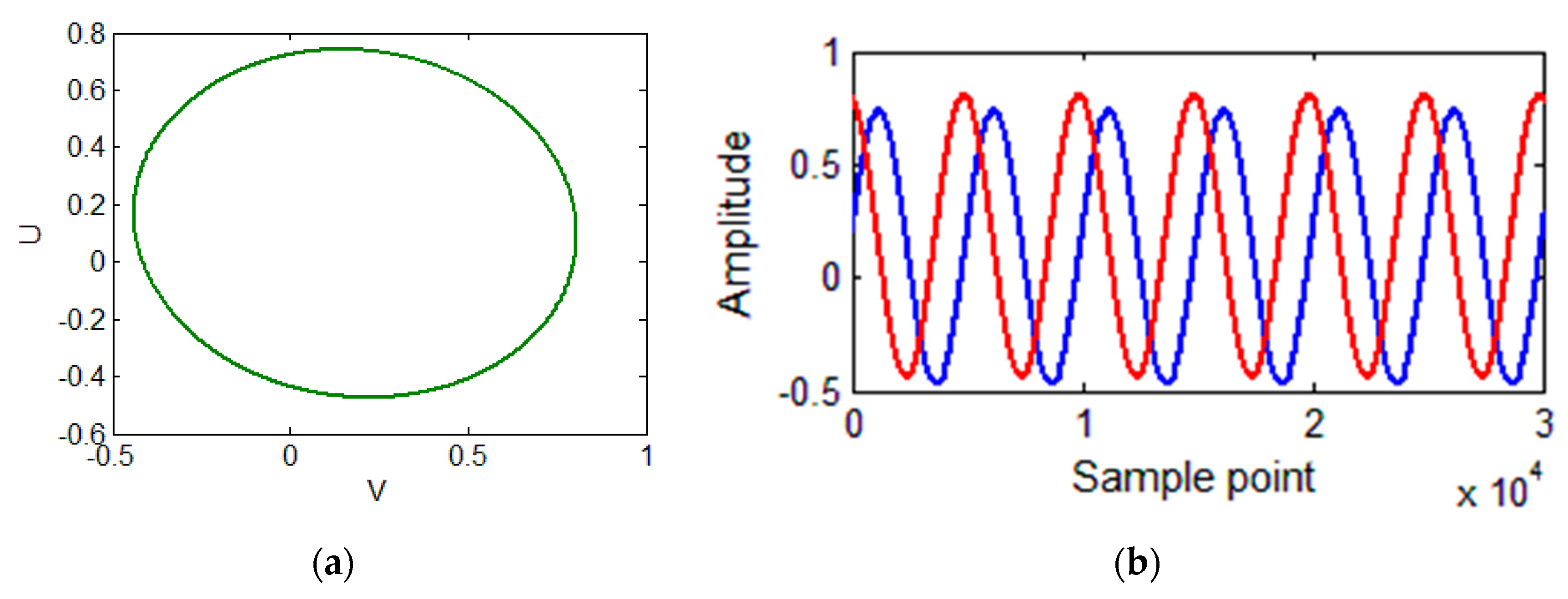
Figure 6 shows the waveform of the simulation signal and the Lissajous figure.
For the LMSED algorithm, the step factor of signal U is set to W 1 = 0.0003 ( 1 , 1 , 1 ) T and that of signal V is set to W 2 = 0.0001 ( 5 , 3 , 1 ) T 
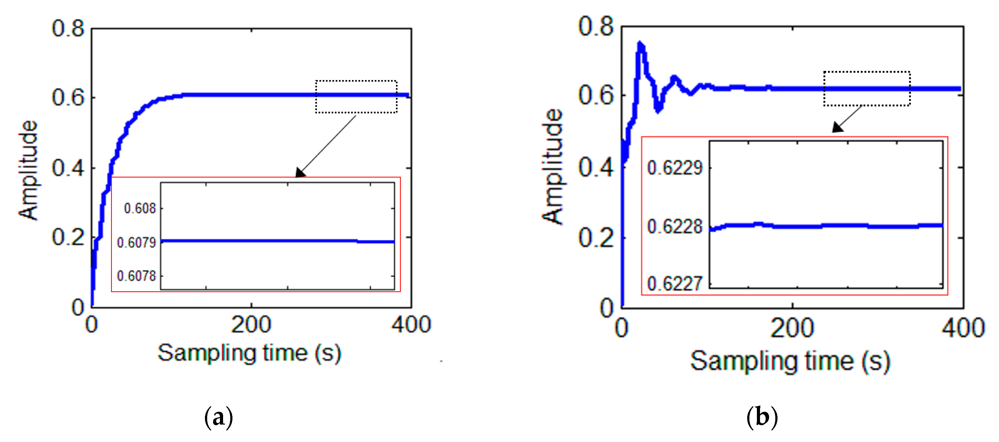
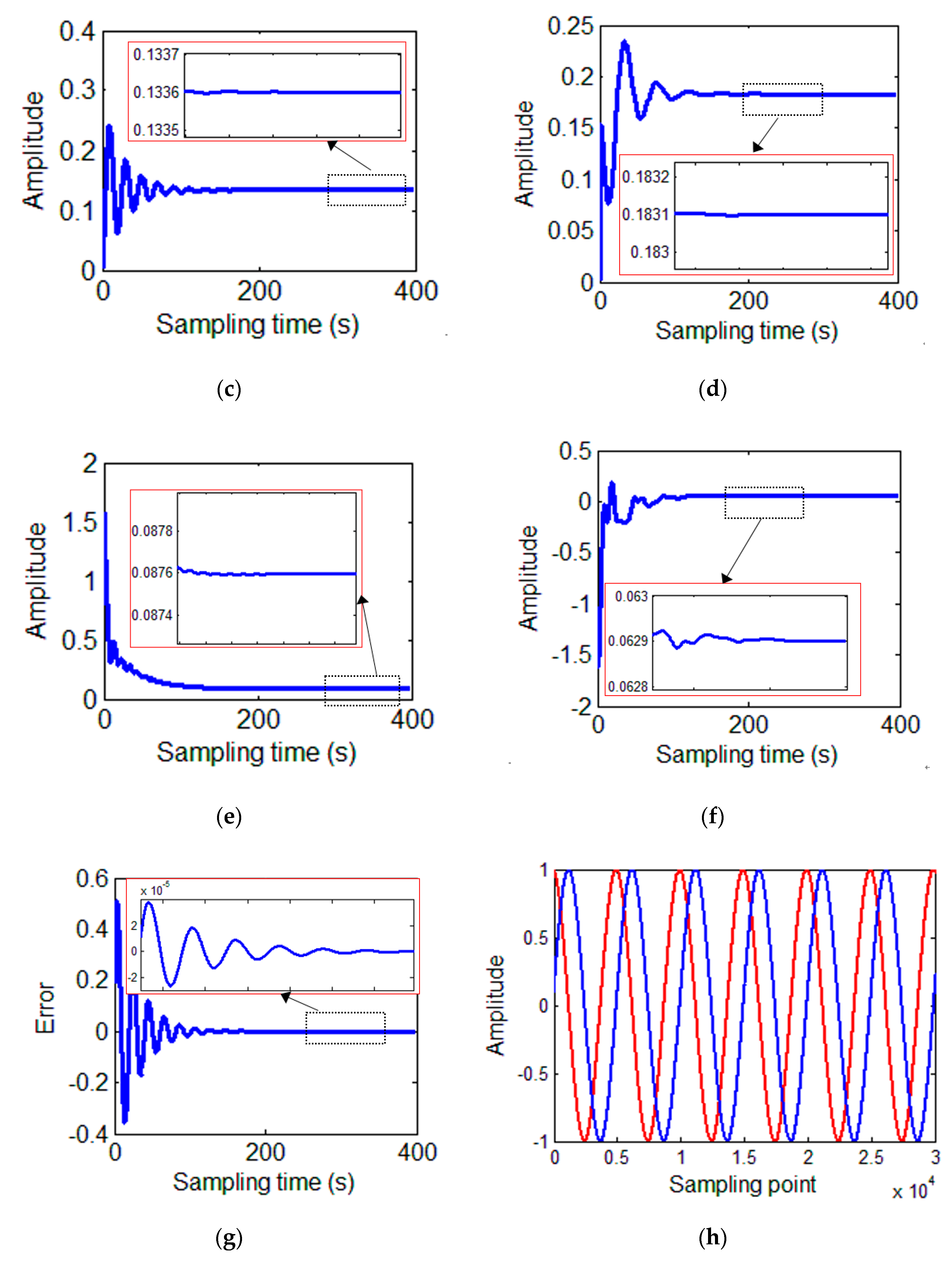
. For the demodulation process, the curve of the parameters, the error curve, and the calibrated signals are shown in Figure 7.
Parameter demodulation results are summarized in Table 1.
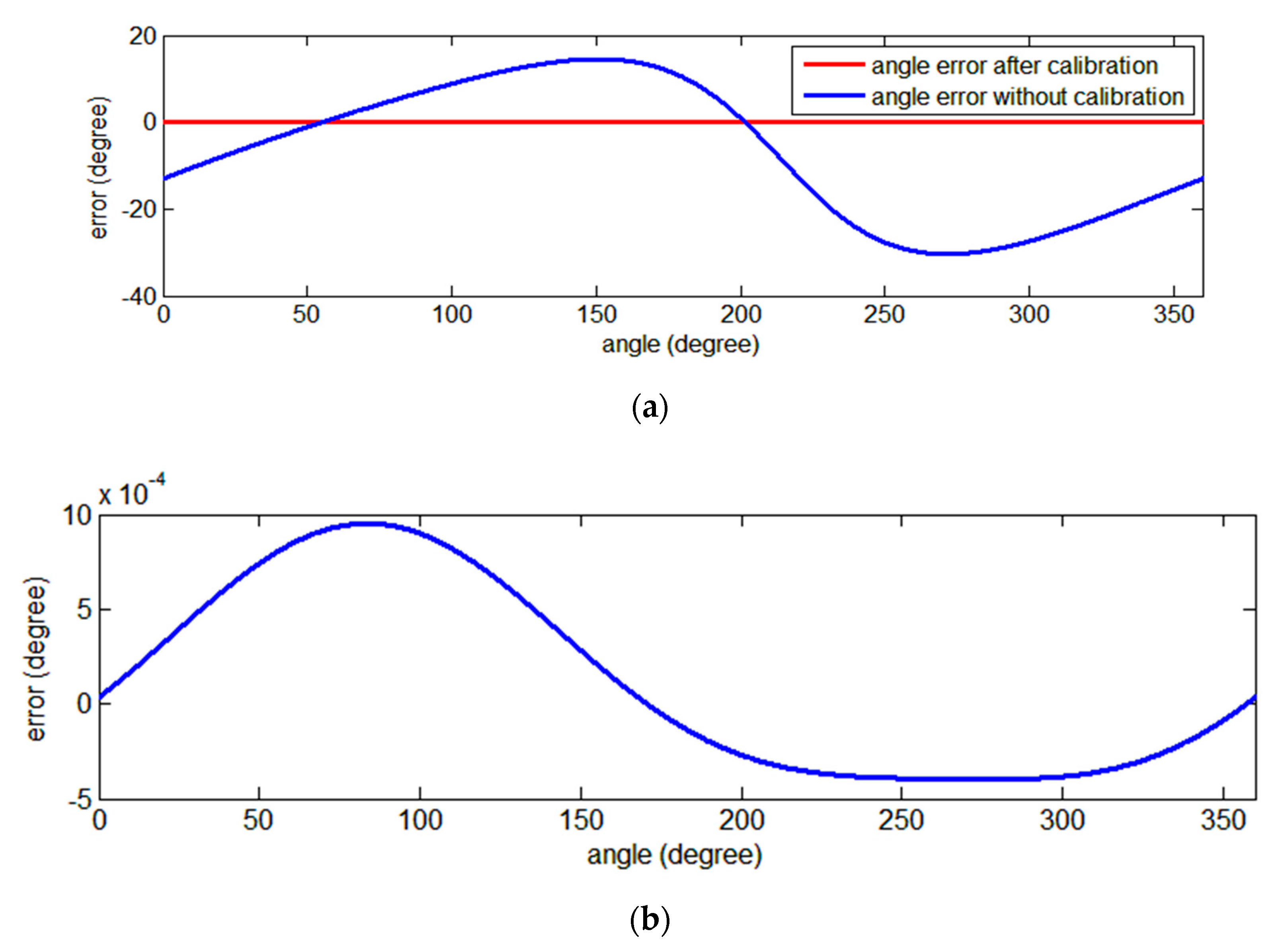
Additionally, the angular calculation errors with and without calibration are shown in Figure 8.
The maximum value of the angular error without and with parameter calibration is 30.38° and 9.52 ×   10 4 °, respectively. The error reduces to 0.003 % after calibration. The results show that the proposed algorithm can accurately calculate the signal component amplitude and also verify the accuracy of the angle calculation module.
When the parameter demodulation values are stable within 1 ± 1 % of the preset values, the steady-state of convergence is reached. Thus, the time when all parameters satisfy this requirement for the first time is defined as the convergence time. In the simulation results, the convergence time is approximately 195.70 s. Based on the iterative formula of the parameters, it can be inferred that sampling frequency, angular frequency, and step factor all have an influence on convergence speed and accuracy. This effect cannot be characterized by a simple function. To control a single variable, more simulation experiments are performed and better optimization parameters and faster convergence speed are obtained. Results are summarized in Table 2. This process is an attempt to continuously change parameters near the initial value. In the experiment, we tried the frequency parameter from 0 to 1000 Hz, and the step factor ranged from 1 × 10 6 to 1.
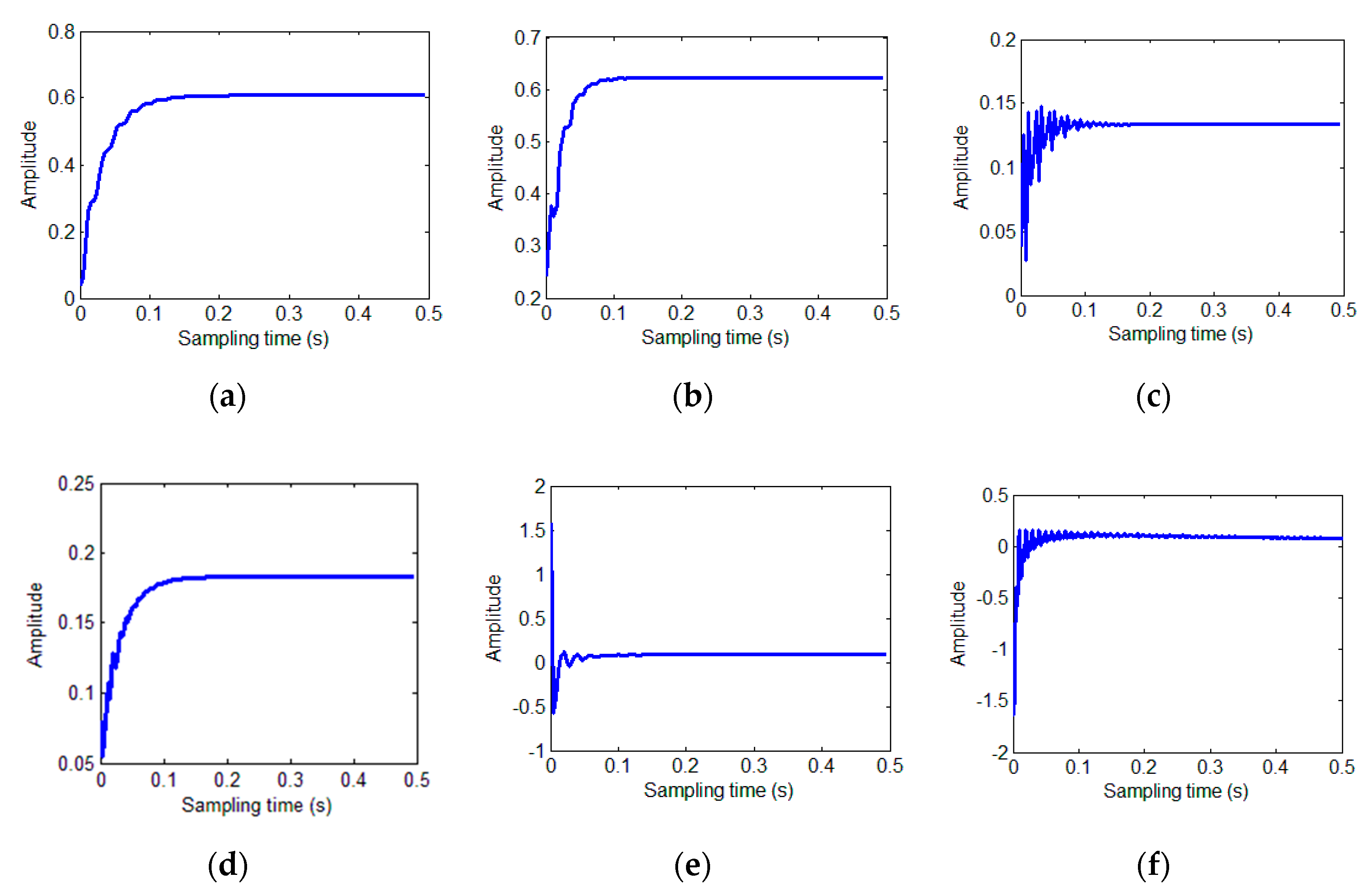
The influence of the step factor is also tested. For a sampling and angular frequency of 250 Hz and 100 Hz, respectively, a faster convergence speed is obtained by changing the step factor. When the step factor is set to W 1 = ( 0.2 , 0.2 , 0.2 ) T and W 2 = ( 0.5 , 0.3 , 0.1 ) T , the convergence time is 0.16 s and the parameters converge to the preset values. The convergence process is shown in Figure 9.
According to the simulation results, the step factor has a greater impact on convergence speed, as properly increasing the step factor speeds up convergence. However, an excessive step factor may cause the parameters to change drastically, causing the entire convergence process to exhibit oscillating changes and prolong convergence time. Figure 7 and Figure 9 are the convergence processes of the demodulation parameters after determining the design parameters. They correspond to different design parameters. Better design parameters can be chosen by controlling a single variable. Since the demodulation method is essentially an iterative algorithm, the relationship between the convergence speed and the design parameters does not have an explicit expression, and can only be qualitatively evaluated. Therefore, the SoC is designed to support software-based configuration of parameters.

4.1.2. Analysis of the Effect of Influencing Factors on Demodulation and Calibration Results

In the section above, the ideal signal model is used and the exact parameter values are obtained, and the error after calibration is almost zero. This section describes the effect of the influencing factors on the calibration effect, including noise and the non-constant rotational speed.
For noise analysis, Gaussian noise with a mean of 0 and a variance of 1 is added to the two signals. The maximum value of the absolute value of the noise is defined as the noise peak, and the influence of the noise peak on the parameter solution and the angle calibration is analyzed.
The simulation signal is described in Equation (21). The input angle and sample frequency is 0.05 and 250 Hz. The range of noise peaks is chosen to be 10 n ( n = 2 , 3 , 6 ) times the amplitude of the simulated signal. n is defined as the noise scale factor. The results when simulation time is 400 s are summarized in Table 3.
The preset values of a 1 , a 2 , b 1 , b 2 , β , φ are 0.6079, 0.6228, 0.1336, 0.1831, 0.0629, 0.0876, respectively. When four decimal places are reserved, the solution result is the same as the set value. For further analysis, the angular position error results with and without calibration are summarized in Table 4, with different noise peak values.
From the simulation results, the existence of noise has little effect on the parameter demodulation, which is related to the characteristics of the demodulation algorithm looking for the average error. The proposed solution does not eliminate signal noise, so the presence of noise affects the accuracy of the calculation of the angle.
For non-constant rotational speed analysis, speed disturbance with a mean of 0 and a variance of 1 is added to the two signals. The simulation signals have expressions described in Equation (22). The range of noise peaks is chosen to be 10 m ( m = 2 , 3 , 4 ) times the value of the simulated frequency. m is defined as the scale factor. The simulation results are summarized in Table 5 and Table 6.
U ( k ) = 0.6079 sin ( ( 2 π f c + μ ( k ) ) k + 0.0876 ) + 0.1336 , V ( k ) = 0.6228 cos ( ( 2 π f c + ν ( k ) ) k + 0.0876 + 0.0629 ) + 0.1831 .
From the simulation results, the disturbance of speed has a great influence on the parameter demodulation. Taking U ( k ) as an example, it can be concluded from Equation (23) that the fluctuation of velocity is equivalent to adding an error component to both the amplitude and the DC offset. When the sampling time is large enough, the amplitude component will have a large change, and the excessive change will invalidate the algorithm.
U ( k ) = a 1 sin ( ( 2 π f c + μ ( k ) ) k + φ ) + b 1 = a 1 cos ( μ ( k ) k ) sin ( 2 π f c k + φ ) + ( b 1 + a 1 sin ( μ ( k ) k ) cos ( 2 π f c k + b 1 ) ) .
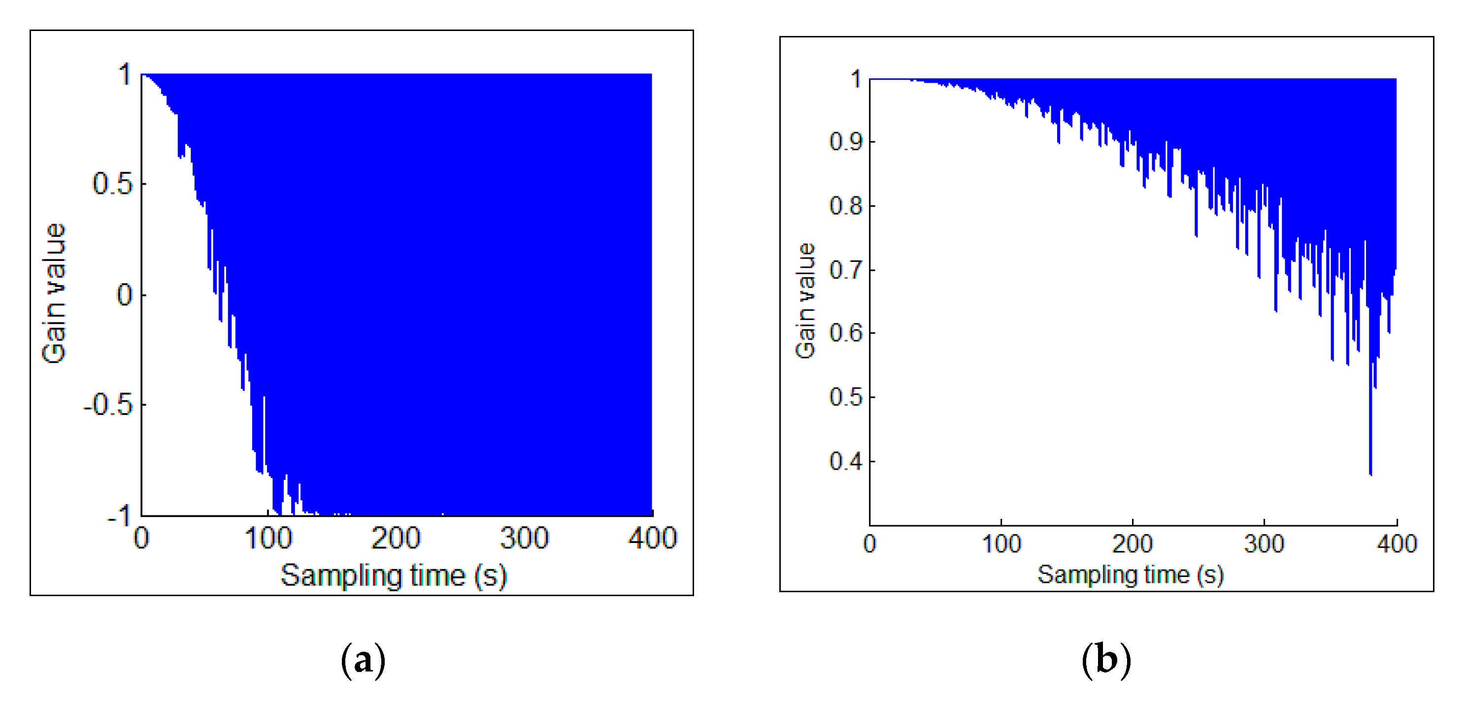
The amplitude gain caused by the speed disturbance is cos ( μ ( k ) k ) . When the scale factor m is −1, −2, −3, −4, the gain curve is shown in Figure 10.
When the speed fluctuation is large ( m = 1 ), the demodulation curve will diverge; when the simulation time is long, the influence of the speed fluctuation on the amplitude becomes obvious, and the parameter demodulation curve diverges as well.
According to the analysis results, since the noise does not change the parameter values, the parameter demodulation process is not sensitive to noise; while the speed disturbance adds error components to the parameters, so the accuracy of the parameter demodulation is affected, and even the algorithm fails.

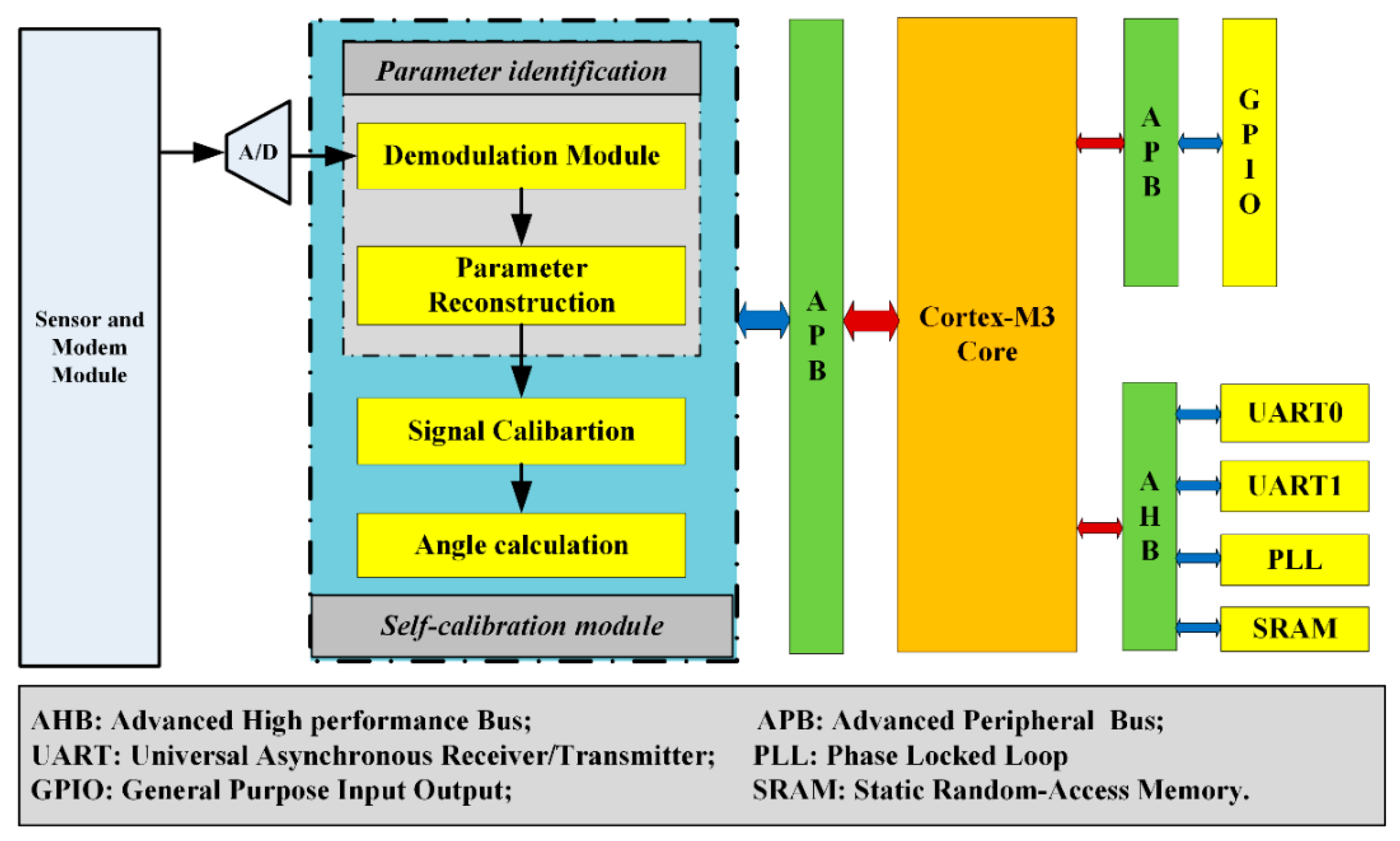
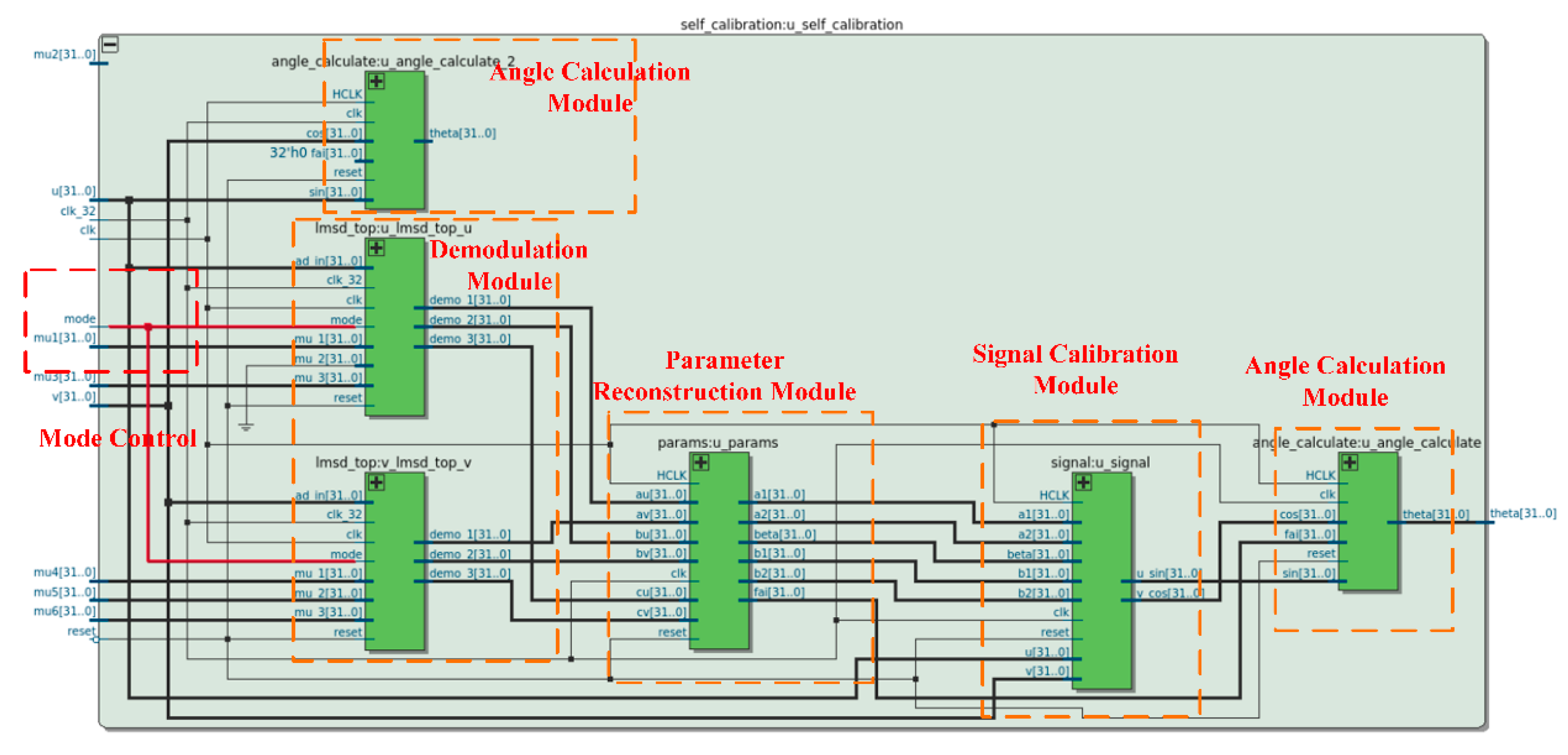
4.2. RTL Simulation of the Self-Calibration Coprocessor

According to the overall scheme design, the architecture of Figure 2 is described using the Verilog hardware description language [27]. The purpose of the RTL simulation is to study the error ratio that the algorithm can reduce errors involving quantization and rounding errors of fixed-point calculation modules (multiplication, root number, and arctangent operations). The RTL view of the coprocessor after synthesis with Altera Quartus II [28] is shown in Figure 11.
The resource overhead results obtained from Quartus synthesis tool and power estimation results from Quartus PowerPlay Power Analyzer Tool are summarized in Table 7.
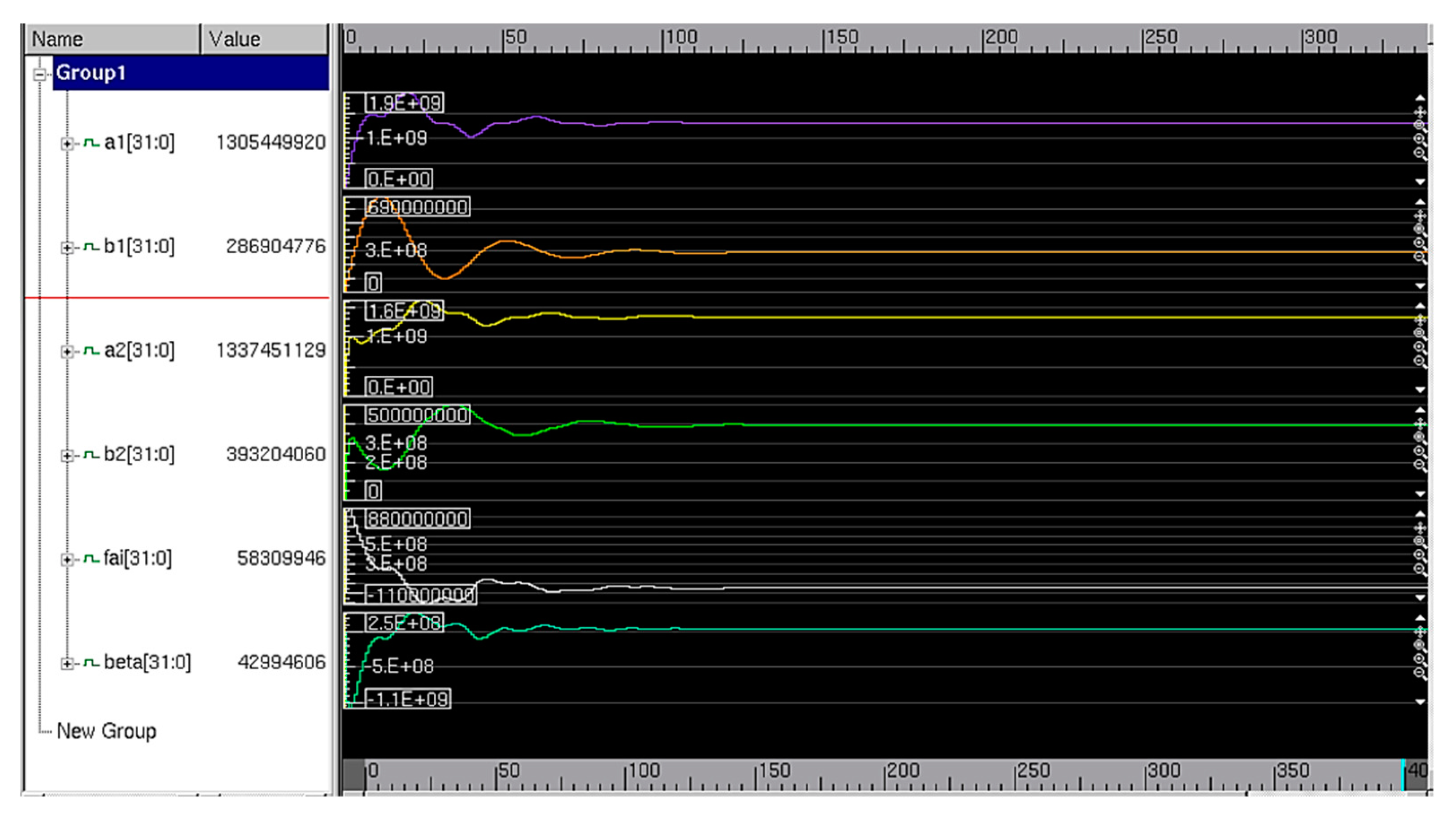
For a sampling frequency of 250 Hz and an angular frequency of 0.05 Hz, the step factor of signal U is set to W 1 = ( 0.2 , 0.2 , 0.2 ) T and the step factor of signal V is set to W 2 = ( 0.5 , 0.3 , 0.1 ) T . The data is quantized using a 32-bit signed fixed-point number with a simulation time set to 400 s. Simulation results are shown in Figure 12.
Specific parameter identification results are shown in Table 8.
The identification values of the amplitude and DC offset are obtained after dividing the identified machine value by 2 31 1 . The identification values of the phase shift are obtained after multiplying the identified machine value by 2 / ( 2 32 1 ) π .
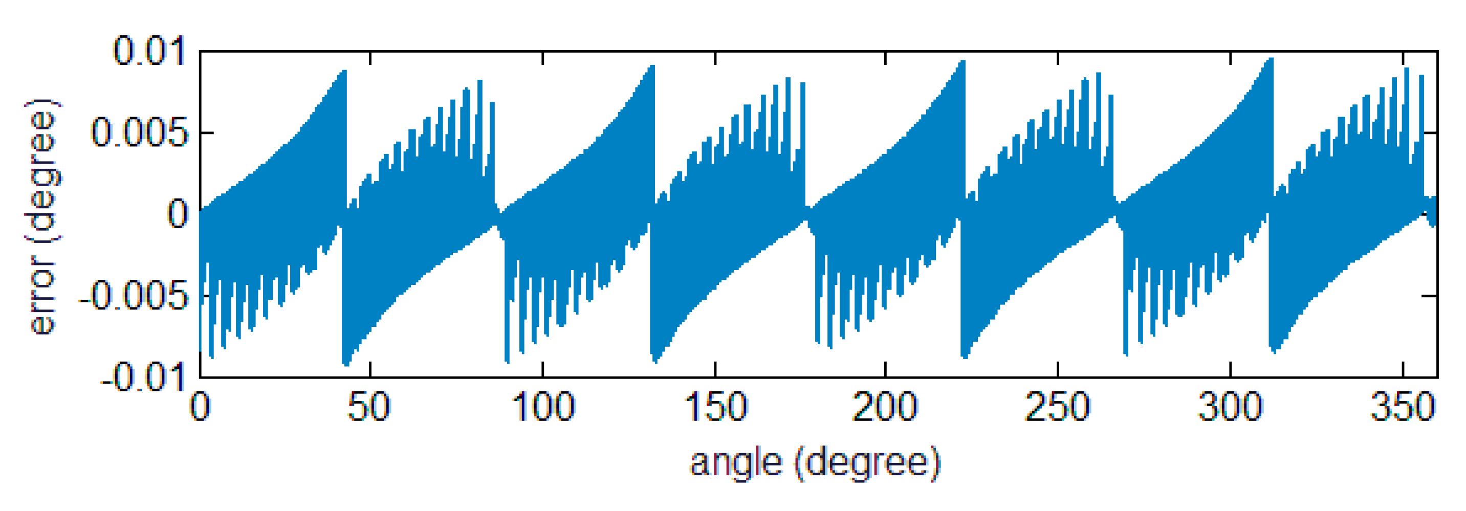
Figure 13 shows the error curve of the angle output by the coprocessor, while the error without calibration is shown in Figure 8a.
The maximum value of the absolute angular error after calibration was 9.50 × 10⁻³°, while the value without calibration was 30.38°, the error reduces to 0.03% of the non-calibration value.
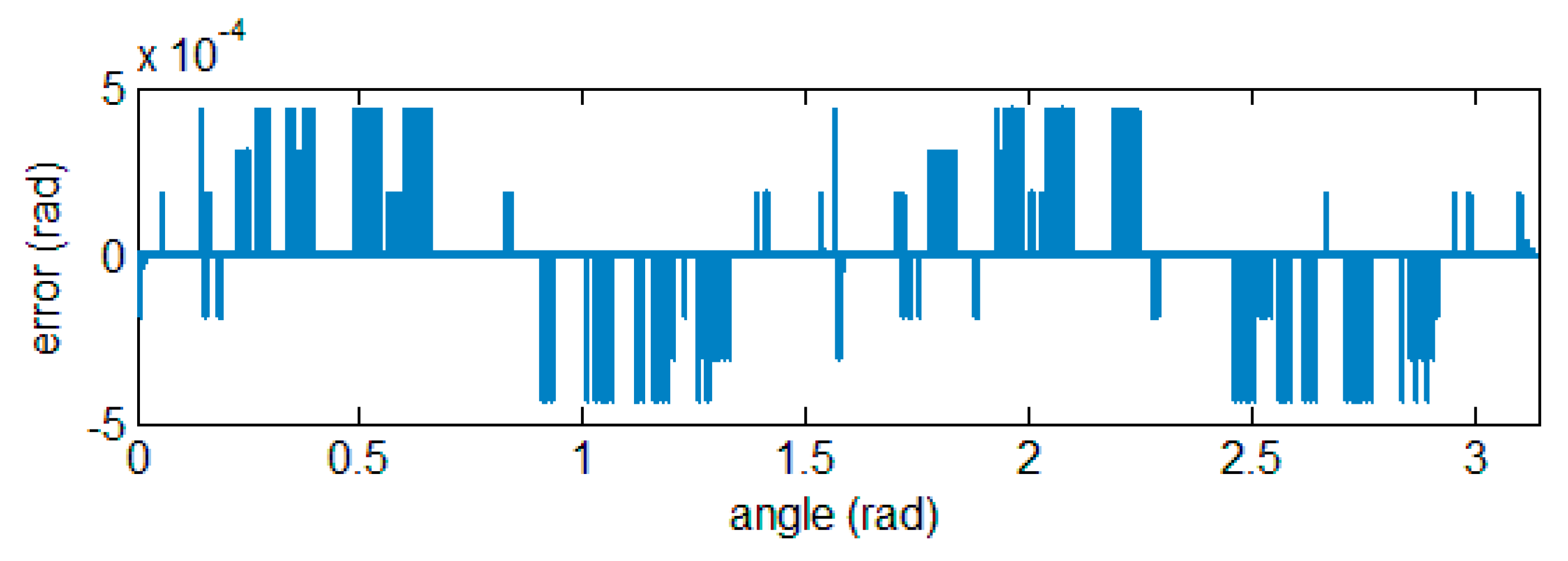
Table 8 shows that the angle-related estimates are not as accurate as the amplitude and DC bias estimates. The angle is calculated by the arctangent module and the calculation error of the arctangent operation is shown in Figure 14. The error is 10 4 orders of magnitude when the operands are sine and cosine functions of magnitude 1.
The accuracy loss in the signal calibration and arctangent modules is one factor that causes the circuit simulation results to be inferior to the MATLAB simulation results. This is mainly related to the multiplication calculation’s rounding error, especially in the arctangent module where 30 multiplication operations are iteratively performed. The circuit optimization of these two parts will be the focus of future work. The results show that the accuracy loss of the calculation modules limits the further improvement of the calibration accuracy. The optimization of these modules is a means for further improved accuracy.

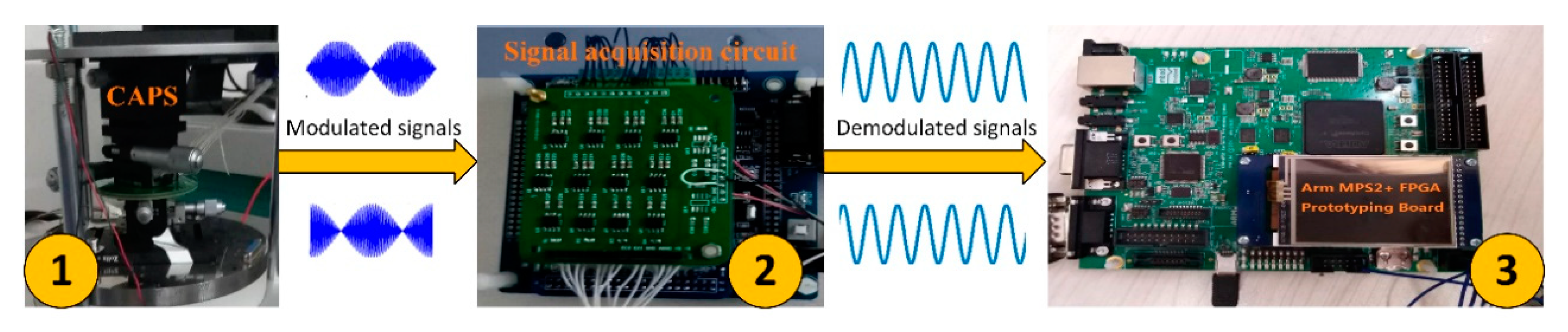
4.3. Experiment Based on FPGA and a CAPS

An experiment is conducted to verify the prototype, and the primary experimental equipment is shown in Figure 15. A CAPS [3] is placed on the turntable (Aviation Industry Co., Beijing, China) and outputs a measurement signal during rotation. The sensitive petal-form electrodes of the CAPS are sine waves in polar coordinates spanning 1 cycles. The signal is demodulated and converted from analog to digital by the signal acquisition circuit. The digital signal is then self-calibrated on the ARM MPS2+ FPGA prototyping board [29] and the drive clock frequency is 25 MHz. The static measurement error of the turntable is about 0.0001 degrees and the dynamic measurement error is about 0.001 degrees, which meets the experimental requirements.
In the self-calibration process, the turntable rotates at 18°/s and the sampling frequency is 250 Hz. The resolution of the acquired angle is 0.072° and the exact values are obtained through the turntable. Figure 16 shows the waveform of the collected signals.
In the experiment, the step factor of signal U is set to W 1 = ( 0.2 , 0.2 , 0.2 ) T and the step factor of signal V is set to W 2 = ( 0.5 , 0.3 , 0.1 ) T 
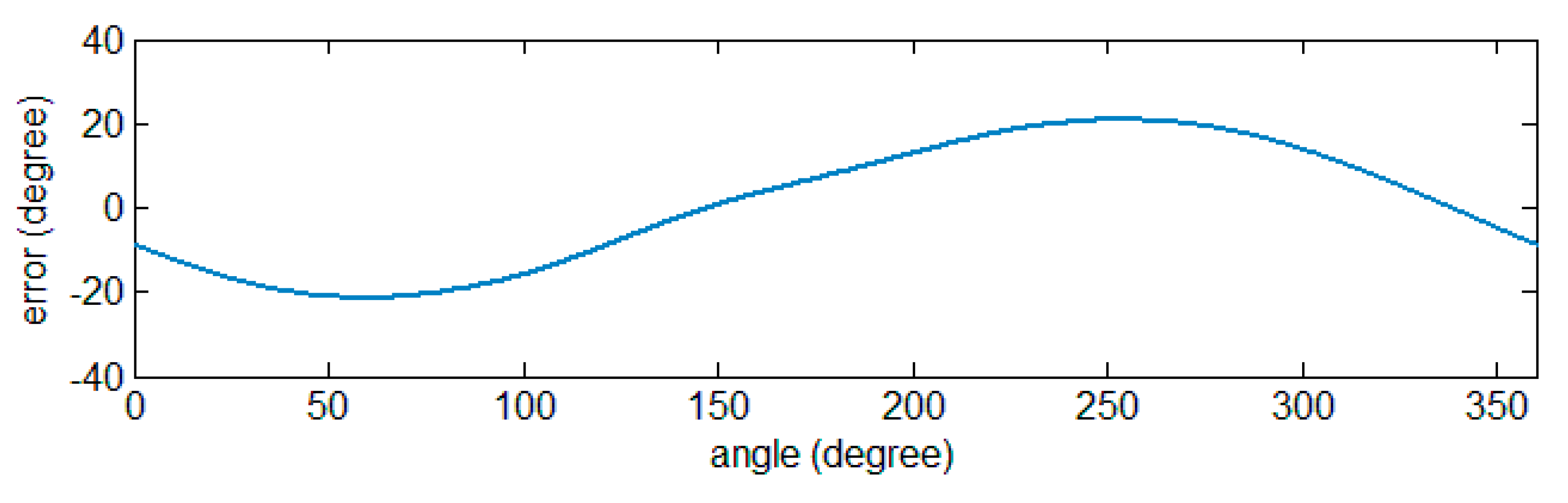
. The angular error without calibration is shown in Figure 17. The peak-to-peak value and maximum absolute value of the error are 43.3964° and 22.5154°, respectively.
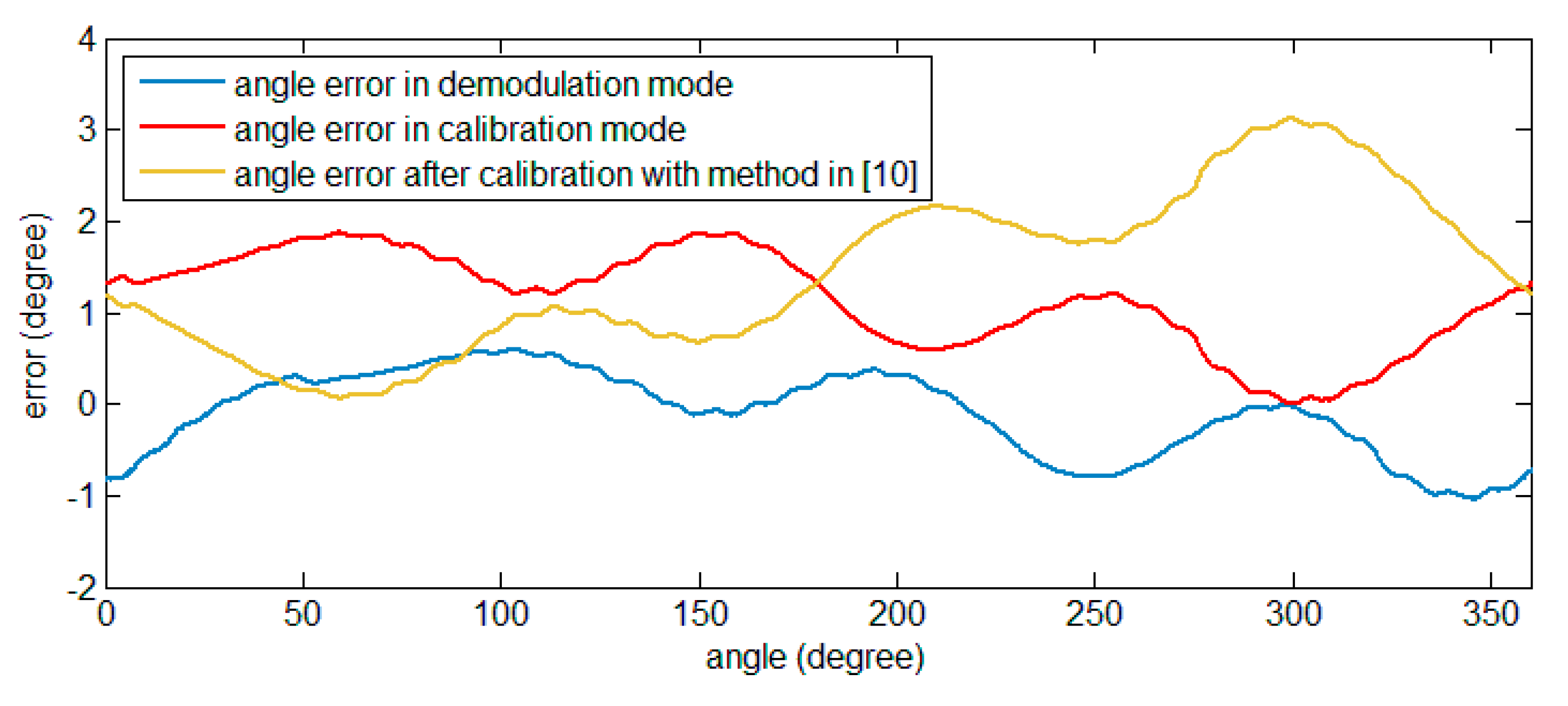
The angle values output by the SoC during the calibration process are also analyzed. The error results are shown in Figure 18, indicated by the angle error curve in demodulation mode for the evaluation of the accuracy of parameter calculations. The peak-to-peak value of the error is 1.7189°, reduced to 3.96%. The maximum absolute value of the error is 0.9814°, reduced to 4.36%.
When the system is operating with angular input that is not continuous, stored parameter values need to be read, and the signal is calibrated using Equation (4). Under this circumstance, the system works in calibration mode. The values of an identified parameter are read through UART (Table 9).
Figure 18 also shows the waveform of this angular error, indicated by the angle error curve in calibration mode. The peak-to-peak value of the error is 1.8683°, reduced to 4.31%. The maximum absolute value of the error is 1.1630°, reduced to 5.17%.
In addition, the signal parameters in the calibration mode can also be obtained by other methods and written in the program; the reference signal frequency in the demodulation mode can also be written in the program to achieve closed-loop control of the frequency estimation.
An experiment for another identification method is carried based on previous work [9], which processes the same error model and the operation is simple. Identification values are summarized in Table 10 and angular error is shown in Figure 18, indicated by the angle error curve after calibration with the method used in [9].
The peak-to-peak value of the error is 3.0617°, reduced to 7.06%. The maximum absolute value of the error is 1.7284°, reduced to 7.68%. The effect of the proposed scheme is not worse than the original work, and even has a better error suppression effect in the experiment.
As for the analysis of execution time, the results are summarized in Table 11 for the proposed scheme and the method in [9], in which the parameter convergence time is defined as the total execution time.
The device in the experiment is a Cyclone V FPGA with a clock frequency of 25 MHz. The algorithm in [9] is executed under the Windows 7 operating system. The programming language is python3.6 and the CPU model is i7-7700K of Intel Corporation, clocked at 4.2 GHz. Since both schemes are iterative algorithms, comparing the execution time of one iteration is beneficial to distinguish the efficiency of the two schemes (the total execution time of the iterative algorithm is affected by the parameters and the actual processed data). Each iteration completes an update of the parameters. In the experiment, the time to complete an iteration is 40 ns at a frequency of 25 MHz. Since the calculation is completed in one clock cycle and the pipeline operation guarantees the data throughput rate, one iteration time is the length of one clock cycle. However, the highest frequency of the circuit design is also affected by the delay of the critical path in the circuit. When using PrimeTime for timing analysis, the maximum frequency of the system is expected to be around 70 MHz. For the execution speed in [9], the total time of 100,000 iterations is calculated and averaged, and the time of a single iteration is 0.464 ms. From this result, the circuit execution speed is faster, but the algorithm in the circuit has low utilization of data, and the parameters are not optimal. These reasons make the total execution time in the experiment longer than that in [9].
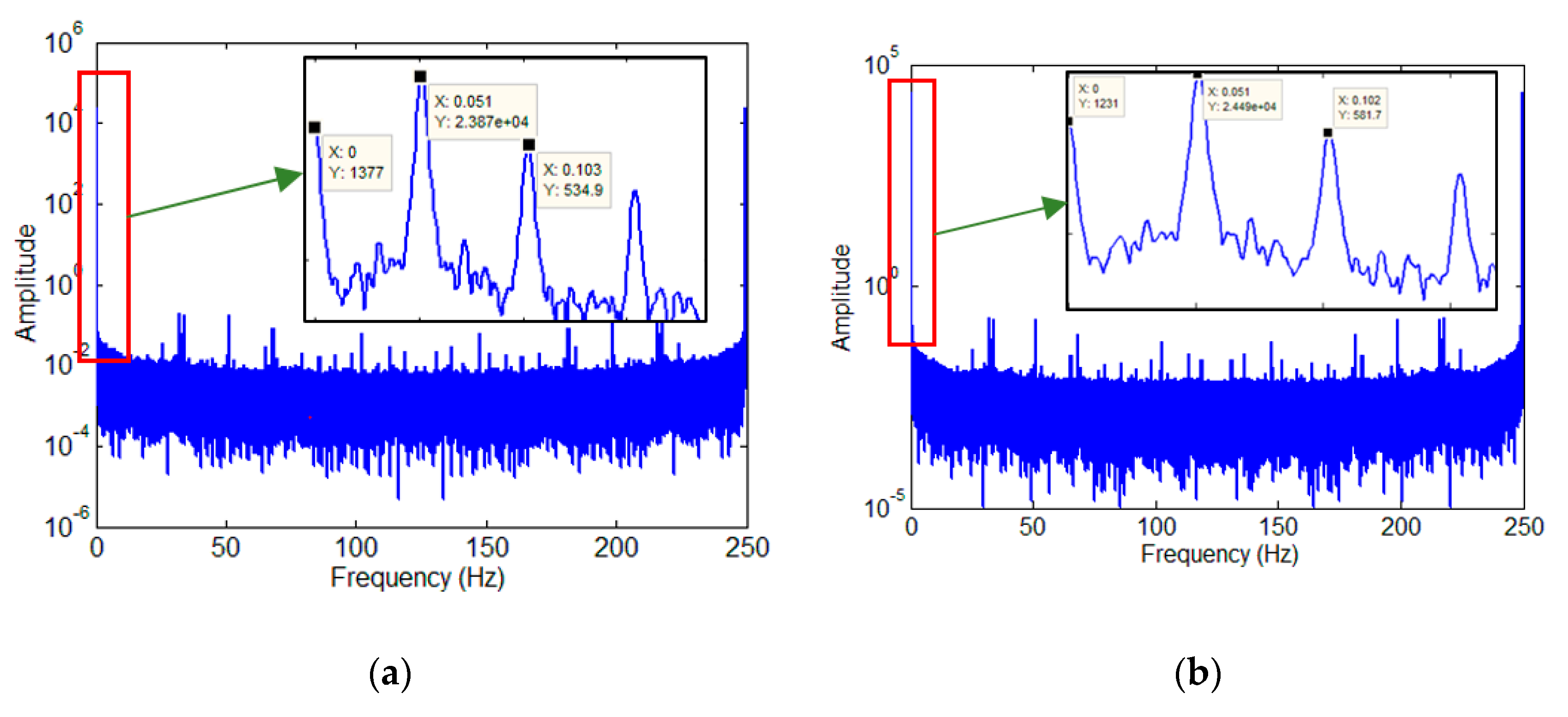
In addition to the velocity analysis, the Fourier analysis of the signal was also carried out. The result is shown in Figure 19. The signal contains harmonic components, and the fundamental frequency value is 0.051 Hz, which deviates from the set value.
In addition, the error curve in the experiment has a certain periodicity, which may be caused by the speed fluctuation and the harmonic component of the signal. It is beyond the capability of the coprocessor and needs to be processed by a more efficient algorithm running in the processor.

5. Conclusions

Self-calibration of angle position sensors is a succinct method in practice. This paper designed a SoC with a calibration coprocessor in it. The SoC is capable of signal processing and transmission at the circuit level and has the ability to implement information fusion algorithms or other secondary development work. The coprocessor integrates a signal demodulation circuit that performs signal component detection using only addition and multiplication operations. On this basis, signal calibration and angle calculation modules are also integrated into the circuit. The entire system was implemented on FPGA and has processed the output signal of the CAPS. In summary, the proposed scheme is based on the design flow of digital integrated circuits, and studies simple but effective algorithms to implement hardware acceleration, and provides a SoC to improve the flexibility of the entire solution.
The calibration algorithm was verified and analyzed using MATLAB. The RTL simulation results of the coprocessor showed that the maximum value of the absolute angle error can be reduced to 0.04%. FPGA-based experiments also confirmed that the SoC can reduce the maximum value of the absolute angle error to 4.36%. Furthermore, results showed that for sensor data collected in the experiments, the peak-to-peak error value was reduced to 3.96% and 4.31% under the SoC demodulation and calibration mode, respectively. Compared with the results of the previous work [9], the proposed scheme can better suppress the angular error.
Accuracy improvement of the calculation modules in the circuit is one example of performance optimization. Optimizing the resource overhead and speed of the modules is also a research direction to improve the performance of the entire system. In addition, the implementation of digital chips for MEMS sensors will also be a focus of future research.

Author Contributions

R.Z. and B.Z. designed the sensor. Z.G. designed the proposed method and performed the experiments. B.H. and C.L. collected the experiment data. Q.W. analyzed the experiment results. B.H. collected literature and evaluated design options. Z.G., B.H., R.Z., B.Z., C.L., B.H., H.S. and Q.W. wrote the paper.

Funding

This research was funded by the National Natural Science Foundation of China, grant number 41871245 and the National High Technology Research and Development Program of China, grant number 2013AA014103.

Acknowledgments

The authors would like to thank Shawn for proofreading and Xiang Li for discussion.

Conflicts of Interest

The authors declare no conflict of interest.

References

  1. Bunte, A.; Beineke, S. High-performance speed measurement by suppression of systematic resolver and encoder errors. IEEE Trans. Ind. Electron. 2004, 51, 0–53. [Google Scholar] [CrossRef]
  2. Benammar, M.; Benbrahim, L.; Alhamadi, M.A. A novel resolver-to-360° linearized converter. IEEE Sens. J. 2004, 4, 96–101. [Google Scholar] [CrossRef]
  3. Bo, H.; Bin, Z.; Mingliang, S. A Novel Single-Excitation Capacitive Angular Position Sensor Design. Sensors 2016, 16, 1196. [Google Scholar]
  4. Dhar, V.K.; Tickoo, A.K.; Kaul, S.K.; Koul, R.; Dubey, B.P. Artificial Neural Network-based error compensation procedure for low-cost encoders. Meas. Sci. Technol. 2009, 21, 209–213. [Google Scholar] [CrossRef]
  5. Tan, K.K.; Tang, K.Z. Adaptive online correction and interpolation of quadrature encoder signals using radial basis functions. IEEE Trans. Control. Syst. Technol. 2005, 13, 370–377. [Google Scholar]
  6. Heydemann, P.L.M. Determination and correction of quadrature fringe measurement errors in interferometers. Appl. Opt. 1981, 20, 3382–3384. [Google Scholar] [CrossRef] [PubMed]
  7. Chuckpaiwong, I. Ellipse fitting method in multidimensional space for on-site sensor calibration. In Proceedings of the IEEE Region 10 Conference (TENCON 2004), Chiang Mai, Thailand, 24–24 November 2004; pp. 685–688. [Google Scholar]
  8. Hoseinnezhad, R. Calibration of Resolver Sensors in Electromechanical Braking Systems: A Modified Recursive Weighted Least-Squares Approach. IEEE Trans. Ind. Electron. 2007, 54, 1052–1060. [Google Scholar] [CrossRef]
  9. Gao, Z.; Zhou, B.; Hou, B.; Li, C.; Wei, Q.; Zhang, R. Self-Calibration of Angular Position Sensors by Signal Flow Networks. Sensors 2018, 18, 2513. [Google Scholar] [CrossRef] [PubMed]
  10. Gao, Z.; Zhou, B.; Hou, B.; Li, C.; Wei, Q.; Zhang, R. Self-Calibration of Nonlinear Signal Model for Angular Position Sensors by Model-Based Automatic Search Algorithm. Sensors 2019, 19, 2760. [Google Scholar] [CrossRef] [PubMed]
  11. Wu, Z.; Li, Y. High-Accuracy Automatic Calibration of Resolver Signals via Two-Step Gradient Estimators. IEEE Sens. J. 2018, 18, 2883–2891. [Google Scholar] [CrossRef]
  12. Hou, M. Amplitude and frequency estimator of a sinusoid. IEEE Trans. Autom. Control. 2005, 50, 855–858. [Google Scholar] [CrossRef]
  13. Hoang, H.V.; Jeon, J.W. Signal compensation and extraction of high resolution position for sinusoidal magnetic encoders. In Proceedings of the IEEE 2007 International Conference on Control, Automation and Systems, Seoul, South Korea, 17–20 October 2007; pp. 1368–1373. [Google Scholar]
  14. Hieu, T.L.; Hung, V.H.; Jae, W.J. Efficient method for correction and interpolation signal of magnetic encoders. In Proceedings of the 2008 6th IEEE International Conference on Industrial Informatics, Daejeon, Korea, 13–16 July 2008; pp. 1383–1388. [Google Scholar]
  15. Kang, H.J.; Kim, S.H.; Lee, S.H. Adaptive digital demodulation of sinusoidal encoder signal for positioning control of spiral servo track writing. Microsyst. Technol. 2012, 18, 1247–1253. [Google Scholar] [CrossRef]
  16. Li, X.; Meijer, G.C.; De Jong, G.W. A microcontroller-based self-calibration technique for a smart capacitive angular-position sensor. In Proceedings of the IEEE Instrumentation & Measurement Technology Conference, Anchorage, AK, USA, 21–23 May 2002; IEEE: Piscataway, NJ, USA, 2002. [Google Scholar]
  17. Cortex-M3. Available online: https://developer.arm.com/ip-products/processors/cortex-m/cortex-m3 (accessed on 9 July 2018).
  18. Smart, D.R. Fixed point theorems. In Cambridge Tracts in Mathematics, 66; Cambridge University Press: Cambridge, UK, 1974. [Google Scholar]
  19. Bennett, S. A brief history of automatic control. IEEE Control Syst. Mag. 1996, 16, 17–25. [Google Scholar]
  20. Variable Resolution, 10-Bit to 16-Bit R/D Converter with Reference Oscillator. Available online: https://www.analog.com/media/en/technical-documentation/data-sheets/AD2S1210.pdf (accessed on 24 April 2019).
  21. Salazar, A.; Bahubalindruno, G.; Locharla, G. A study on look-up table based sine wave generation. In Proceedings of the Regional Echomail Coordinator, Porto, Portugal, 3–4 February 2011. [Google Scholar]
  22. Yanxin, L.; Aiqun, H. An Adaptive Demodulation Method for QAM Signals. In Proceedings of the 2007 International Symposium on Microwave, Antenna, Propagation and EMC Technologies for Wireless Communications, Hangzhou, China, 16–17 August 2007. [Google Scholar]
  23. Goh, W.B. Noise robust AM_FM demodulation using least- squares truncated power series approximation. In Proceedings of the International Conference on Information, Singapore, 10–13 December 2007; IEEE: Piscataway, NJ, USA, 2008. [Google Scholar]
  24. Richter, P.H. Estimating Errors in Least-Squares Fitting; Telecommunications and Data Acquisition Progress Report. Available online: https://ntrs.nasa.gov/archive/nasa/casi.ntrs.nasa.gov/19960009481.pdf (accessed on 11 March 2019).
  25. Garcia, E.O.; Cumplido, R.; Arias, M. Pipelined CORDIC design on FPGA for a digital sine and cosine waves generator. In Proceedings of the International Conference on Electrical & Electronics Engineering, Veracruz, Mexico, 6–8 September 2006; IEEE: Piscataway, NJ, USA, 2006. [Google Scholar]
  26. Dai, Y.; Yuan, J.; Yuan, Y.X. Modified Two-Point Stepsize Gradient Methods for Unconstrained Optimization. Comput. Optim. Appl. 2002, 22, 103–109. [Google Scholar] [CrossRef]
  27. Automation, D.; Committee, S. IEEE Standard for Verilog Hardware Description Language; IEEE Std 1364-2005 (Revision of IEEE Std 1364-2001); IEEE: Piscataway, NJ, USA, 2006. [Google Scholar]
  28. Intel® FPGA Development Tools. Available online: https://www.intel.com/content/www/us/en/software/programmable/quartus-prime/download.html (accessed on 3 December 2018).
  29. Arm MPS2 + FPGA Prototyping Board. Available online: https://developer.arm.com/products/system-design/development-boards/fpga-prototyping-boards/mps2 (accessed on 19 July 2018).
Figure 1. Working principle of the Capacitive Angular Position Sensors (CAPS).
Applsci 09 04772 g001
Figure 2. Architecture of the proposed System-on-Chip (SoC).
Applsci 09 04772 g002
Figure 3. Architecture of the proposed coprocessor.
Applsci 09 04772 g003
Figure 4. Architecture of arctangent operation module based on a proportional-integral (PI) controller.
Applsci 09 04772 g004
Figure 5. Working principle of the Least Mean Square Error Demodulation (LMSED) algorithm.
Applsci 09 04772 g005
Figure 6. Simulation signals: (a) Lissajous figure; (b) waveform of the signals in which the blue curve indicates the sine signal and the red curve indicates the cosine curve.
Applsci 09 04772 g006
Figure 7. Demodulation details. (a) Change process of a 1 ; (b) change process of a 2 ; (c) change process of b 1 ; (d) change process of b 2 ; (e) change process of φ ; (f) change process of β ; (g) change process of calculated error; (h) waveform of the calibrated signals in which the blue and red curve indicates the sine and cosine signal, respectively.
Applsci 09 04772 g007aApplsci 09 04772 g007b
Figure 8. Angular error obtained from the simulation: (a) comparison of angular errors with and without parameter calibration; (b) magnified display of the curve of angular error with parameter calibration in (a).
Applsci 09 04772 g008
Figure 9. Convergence details under better step factors. (a) Change process of a 1 ; (b) change process of a 2 ; (c) change process of b 1 ; (d) change process of b 2 ; (e) change process of φ ; (f) change process of β .
Applsci 09 04772 g009
Figure 10. Amplitude gain due to velocity disturbance: (a) gain curve when m = 1 ; (b) gain curve when m = 2 ; (c) gain curve when m = 3 ; (d) gain curve when m = 4 .
Applsci 09 04772 g010aApplsci 09 04772 g010b
Figure 11. Register-Transfer Level (RTL) view of the designed coprocessor.
Applsci 09 04772 g011
Figure 12. Convergence process of parameter values in the RTL simulation.
Applsci 09 04772 g012
Figure 13. Angular error obtained in the RTL simulation.
Applsci 09 04772 g013
Figure 14. Arctangent operation error in the RTL simulation.
Applsci 09 04772 g014
Figure 15. Experimental equipment including a CAPS, signal acquisition circuit, and a Field Programmable Gate Array (FPGA) on which the SoC is implanted.
Applsci 09 04772 g015
Figure 16. Waveform of the collected signals.
Applsci 09 04772 g016
Figure 17. Angular error without calibration in experiment.
Applsci 09 04772 g017
Figure 18. Angle error curves under different conditions.
Applsci 09 04772 g018
Figure 19. Amplitude spectrum of two signals. (a) Amplitude spectrum of the sine channel; (b) amplitude spectrum of the cosine channel.
Applsci 09 04772 g019
Table 1. Parameter identification results for the simulation.
ParametersPreset ValuesIdentification Values
a 1 0.60790.6079
a 2 0.62280.6228
b 1 0.13360.1336
b 2 0.18310.1831
β 0.06290.0629
φ 0.08760.0876
Table 2. Better variable values with an unchanged step factor in the simulation.
Variable/HzBetter ValueConvergence Time (s)Other Parameter
Sampling frequency f s 325148.80 f c = 0.05
Angular frequency f c 100122.50 f s = 250
Table 3. Analysis of the effect of noise peaks on the demodulation results.
Noise   Scale   Factor   ( n ) Calculated   Value   ( a 1 ) Calculated   Value   ( a 2 ) Calculated   Value   ( b 1 ) Calculated   Value   ( b 2 ) Calculated   Value   ( β ) Calculated   Value   ( φ )
−20.60790.62280.13360.18310.06290.0876
−30.60790.62280.13360.18310.06290.0876
−40.60790.62280.13360.18310.06290.0876
−50.60790.62280.13360.18310.06290.0876
−60.60790.62280.13360.18310.06290.0876
Table 4. Analysis of the effect of noise peaks on the calibration results.
Noise   Scale   Factor   ( n ) Maximum Value of the Absolute Error without Calibration Maximum Value of the Angular Error with CalibrationError Reduction Ratio
−230.78°0.60°1.95%
−330.42°0.06°0.20%
−430.39°0.06°0.02%
−530.38° 1.50 × 10 3 °0.005%
−630.38° 9.94 × 10 4 °0.003%
Table 5. Analysis of the effect of speed disturbance on the demodulation results.
Scale   Factor   ( m ) Calculated   Value   ( a 1 ) Calculated   Value   ( a 2 ) Calculated   Value   ( b 1 ) Calculated   Value   ( b 2 ) Calculated   Value   ( β ) Calculated   Value   ( φ )
−20.58660.59990.13250.18170.06700.0866
−30.60790.62270.13360.18300.06270.0877
−40.60790.62280.13360.18310.06290.0876
Table 6. Analysis of the effect of speed disturbance on the calibration results.
Scale   Factor   ( m ) Maximum Value of the Absolute Error without Calibration Maximum Value of the Angular Error with CalibrationError Reduction Ratio
−234.81°1.12°3.27%
−330.58°0.17°0.55%
−430.25°0.03°0.09%
Table 7. Resource overhead and power estimation results.
CategoryResults
Logic Utilization (in ALMs)12,192
Total Registers7106
Total Pins233
Total DSP Blocks125
Thermal Power Estimation (mW)361.875
Table 8. Results at 400 s in the RTL simulation.
ParametersPreset ValuesMachine ValuesIdentification ValuesRelative Error
a 1 0.60791,305,449,9200.60780.0004%
a 2 0.62281,337,451,1290.62270.0001%
b 1 0.1336286,904,7760.1336−0.0003%
b 2 0.1831393,204,0600.18310.0001%
β 0.062942,994,6060.06290.0038%
φ 0.087658,309,9460.08532.6225%
Table 9. Parameter identification values obtained from the experiment.
ParametersMachine ValuesIdentification Values
a 1 1,308,364,5800.6039
a 2 1,336,685,2450.6224
b 1 274,228,3300.1277
b 2 388,108,7000.1807
β 2,105,078,0193.0796
φ 3,700,681,6505.4138
Table 10. Parameter identification values obtained based on technology detailed in [9].
ParametersIdentification Values
a 1 0.6085
a 2 0.6221
b 1 0.1323
b 2 0.1834
β 3.0734
Table 11. Results about execution time in experiments.
MethodDeviceTotal Execution Time Execution Time for One Iteration
Proposed methodCyclone V FPGA [29]197.83 s40 ns
Method in [9]Laptop46.42 s0.46 ms

