An Internal Folded Hardware-Efficient Architecture for Lifting-Based Multi-Level 2-D 9/7 DWT


Abstract
Featured Application
Abstract
1. Introduction
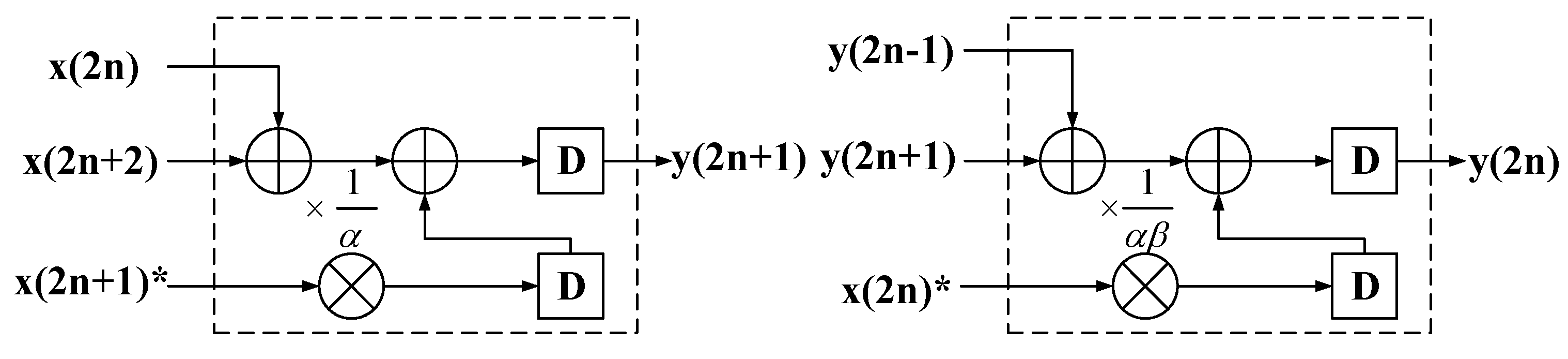
2. Lifting Scheme
3. Proposed Architecture for Muti-Level 2-D DWT
3.1. Data Scanning Method
3.2. Unfolded Architecture
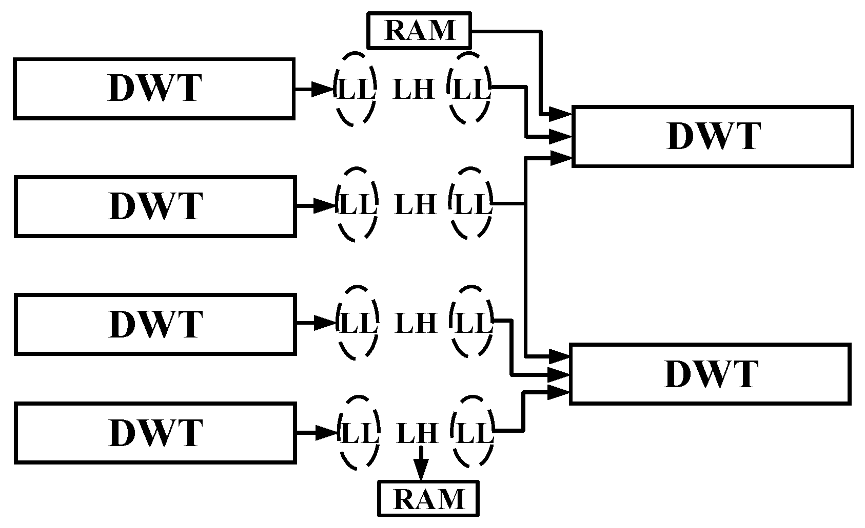
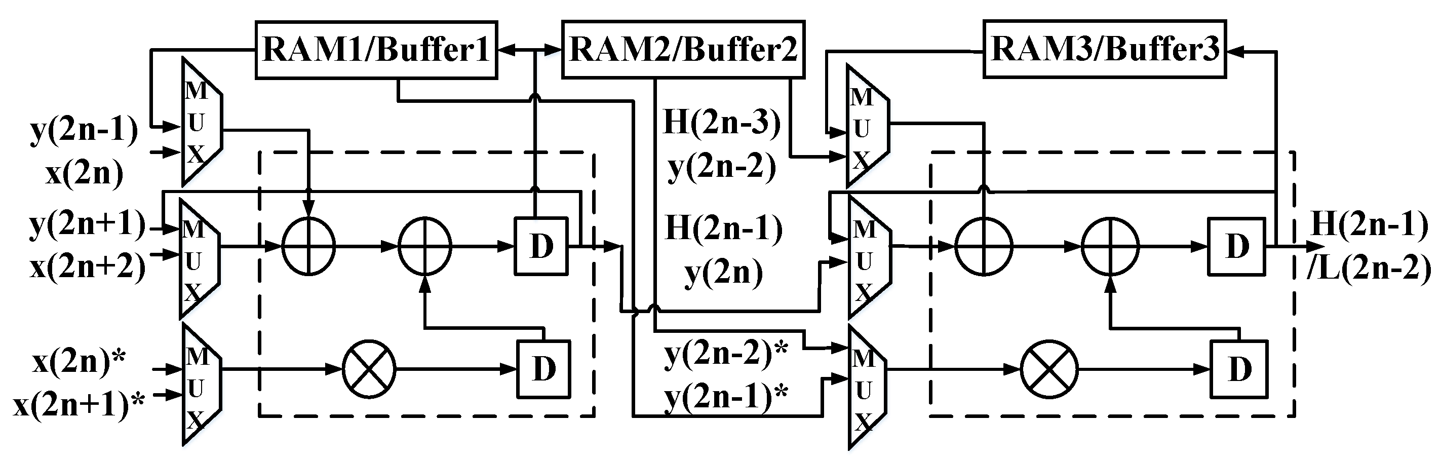
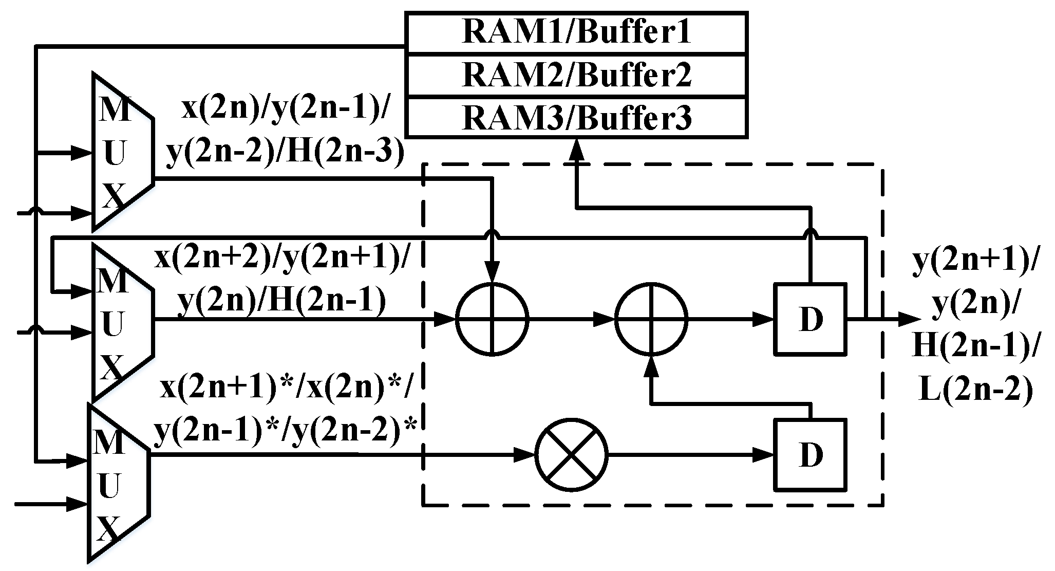
3.3. Proposed Multi-Level DWT Architecture
4. Hardware Estimation and Comparison
4.1. Hardware Estimation
4.2. Performance Comparison
5. Conclusions
Author Contributions
Funding
Acknowledgments
Conflicts of Interest
References
- Zhang, W.; Jiang, Z.; Gao, Z.; Liu, Y. An efficient VLSI architecture for lifting-based discrete wavelet transform. IEEE Trans. Circuits Syst. II Exp. Briefs 2012, 59, 158–162. [Google Scholar] [CrossRef]
- Darji, A.; Agrawal, S.; Oza, A. Dual-Scan parallel flipping architecture for a lifting-Based 2-D discrete wavelet transform. IEEE Trans. Circuits Syst. II Exp. Briefs 2014, 61, 433–437. [Google Scholar] [CrossRef]
- Hu, Y.; Jong, C. A memory-efficient scalable architecture for lifting-Based discrete wavelet transform. IEEE Trans. Circuits Syst. II Exp. Briefs 2013, 60, 502–506. [Google Scholar] [CrossRef]
- Mohanty, B.K.; Meher, P.K. Area-delay-power-efficient architecture for folded two-dimensional discrete wavelet transform by multiple lifting computation. IET Image Process. 2014, 8, 345–353. [Google Scholar] [CrossRef]
- Mohanty, B.K.; Meher, P.K.; Srikanthan, T. Critical-path optimization for efficient hardware realization of lifting and flipping DWTs. In Proceedings of the IEEE ISCAS, Lisbon, Portugal, 24–27 May 2015; pp. 1186–1189. [Google Scholar]
- Todkar, S.; Shastry, P.V.S. Flipping based high performance pipelined VLSI architecture for 2-D discrete wavelet transform. In Proceedings of the IEEE iCATccT, Davangere, India, 29–31 October 2015; pp. 832–836. [Google Scholar]
- Darji, A.; Limaye, A. Memory efficient VLSI architecture for lifting-based DWT. In Proceedings of the IEEE MWSCAS, College Station, TX, USA, 3 August 2014; pp. 189–192. [Google Scholar]
- Tian, X.; Wu, L.; Tan, Y.H.; Tian, J.W. Efficient multi-input/multioutput VLSI architecture for 2-D lifting-based discrete wavelet transform. IEEE Trans. Comput. 2011, 60, 1207–1211. [Google Scholar] [CrossRef]
- Mohanty, B.K.; Meher, P.K. Memory efficient modular VLSI architecture for high throughput and Low-Latency Implementation of Multilevel Lifting 2-D DWT. IEEE Trans. Signal Process. 2011, 59, 2072–2084. [Google Scholar] [CrossRef]
- Mohanty, B.K.; Meher, P.K. Memory-Efficient High-Speed Convolution-Based Generic Structure for Multilevel 2-D DWT. IEEE Trans. Circuits Syst. Video Technol. 2013, 23, 353–363. [Google Scholar] [CrossRef]
- Hu, Y.; Prasanna, V.K. Energy- and area-efficient parameterized lifting-based 2-D DWT architecture on FPGA. In Proceedings of the IEEE HPEC, Waltham, MA, USA, 9–11 September 2014; pp. 1–6. [Google Scholar]
- Hu, Y.; Jong, C. A Memory-Efficient High-Throughput Architecture for Lifting-Based Multi-Level 2-D DWT. IEEE Trans. Signal Process. 2013, 61, 4975–4987. [Google Scholar] [CrossRef]
- Ye, L.; Hou, Z. Memory Efficient Multilevel Discrete Wavelet Transform Schemes for JPEG2000. IEEE Trans. Circuits Syst. Video Technol. 2015, 25, 1773–1785. [Google Scholar] [CrossRef]
- Wu, C.; Zhang, W.; Jia, Q.; Liu, Y. Hardware Efficient Multiplier-less Multi-level 2D DWT Architecture without off-chip RAM. IET Image Process. 2017, 11, 362–369. [Google Scholar] [CrossRef]
- Chakraborty, A.; Chakraborty, D.; Banerjee, A. A multiplier less VLSI architecture of modified lifting based 1D/2D DWT using speculative adder. In Proceedings of the International Conference on Communication and Signal Processing, Chennai, India, 6–8 April 2017. [Google Scholar]
- Anirban, C.; Ayan, B. Low Area & Memory Efficient VLSI Architecture of 1D/2D DWT for Real Time Image Decomposition. In Proceedings of the 2018 8th International Symposium on Embedded Computing and System Design (ISED), Cochin, India, 13–15 December 2018. [Google Scholar]
- Abhishek, C.; Basant, K.M. A Block based Area-Delay Efficient Architecture for Multi-Level Lifting 2-D DWT. Springer Nat. 2018, 37, 4482–4503. [Google Scholar]
- Huang, C.-T.; Tseng, P.-C.; Chen, L.-G. Flipping structure: An efficient VLSI architecture for lifting-based discrete wavelet transform. IEEE Trans. Signal Process. 2004, 52, 1080–1089. [Google Scholar] [CrossRef]
- Emanuel, G. Harmonic Sierpinski Gasket and Applications. Entropy 2018, 20, 714. [Google Scholar]
- Taubman, D.S.; Marcellin, M.W. Jpeg2000: Image Compression Fundamentals, Standards and Practice; Kluwer: Norwell, MA, USA, 2001. [Google Scholar]
- Frongillo, M.; Gennarelli, G.; Riccio, G. TD-UAPO diffracted field evaluation for penetrable wedges with acute apex angle. J. Opt. Soc. Am. A 2015, 32, 1271–1274. [Google Scholar] [CrossRef] [PubMed]


| Architecture | Multiplier | Adder | Register | Temporal RAM (in Word) | Parallelism |
|---|---|---|---|---|---|
| 1:1 | 10 | 16 | 28 | 3N | S |
| 2:1 | 5 | 8 | 33 | 2N | S/2 |
| 4:1 | 3 | 4 | 51 | N | S/4 |
| 3-level | 53S/4 | 21S | 229S/4 | 6N | - |
| Architecture | S | Throughout Rate | Multiplier | Adder | Register | MEM Words | CPD | TC (×106) | ACT | TDP |
|---|---|---|---|---|---|---|---|---|---|---|
| [14] * | 1 | 2/Ta | 0 | 123 | 167 | 3840 | Ta | 0.509 | 131,072 | 200.93 |
| [8] | 8 | 4/Ta | 96 | 128 | 6304 | 82,144 | 4Ta | 10.13 | 21,504 | 2621.69 |
| [9] | 8 | 4/Ta | 99 | 176 | 158 | 5696 | 4Ta | 1.26 | 16,384 | 247.63 |
| [10] | 8 | 8/Ta | 189 | 294 | 443 | 2688 | 2Ta | 1.62 | 16,384 | 160.13 |
| [12] | 8 | 16/3Ta | 111 | 180 | 341 | 1536 | 3Ta | 0.975 | 16,384 | 144.18 |
| Proposed | 8 | 8/Ta | 106 | 168 | 458 | 3072 | 2Ta | 1.12 | 16,384 | 110.17 |
| [12] | 16 | 32/3Ta | 216 | 348 | 682 | 1536 | 3Ta | 1.76 | 8192 | 130.30 |
| [17] | x | 64/3Ta | 0 | 1280 | x | 30,016 | 3Ta | x | 4096 | x |
| Proposed | 16 | 16/Ta | 212 | 336 | 916 | 3072 | 2Ta | 1.94 | 8192 | 95.64 |
| Architecture | S | DAT (ns) | Area (μm2) | Power (mw) | ADP (μm2) | EPI (μJ) |
|---|---|---|---|---|---|---|
| [8] | 8 | 42.66 | 3,377,870.70 | 24.45 | 3098.72 | 26.28 |
| [9] | 8 | 45.58 | 3,104,371.05 | 22.59 | 2318.29 | 18.50 |
| [10] | 8 | 25.42 | 2,139,397.29 | 15.26 | 891.01 | 12.50 |
| Proposed | 8 | 27.70 | 1,362,035.87 | 12.94 | 618.14 | 10.60 |
© 2019 by the authors. Licensee MDPI, Basel, Switzerland. This article is an open access article distributed under the terms and conditions of the Creative Commons Attribution (CC BY) license (http://creativecommons.org/licenses/by/4.0/).
Share and Cite
Zhang, W.; Wu, C.; Zhang, P.; Liu, Y. An Internal Folded Hardware-Efficient Architecture for Lifting-Based Multi-Level 2-D 9/7 DWT. Appl. Sci. 2019, 9, 4635. https://doi.org/10.3390/app9214635
Zhang W, Wu C, Zhang P, Liu Y. An Internal Folded Hardware-Efficient Architecture for Lifting-Based Multi-Level 2-D 9/7 DWT. Applied Sciences. 2019; 9(21):4635. https://doi.org/10.3390/app9214635
Chicago/Turabian StyleZhang, Wei, Changkun Wu, Pan Zhang, and Yanyan Liu. 2019. "An Internal Folded Hardware-Efficient Architecture for Lifting-Based Multi-Level 2-D 9/7 DWT" Applied Sciences 9, no. 21: 4635. https://doi.org/10.3390/app9214635
APA StyleZhang, W., Wu, C., Zhang, P., & Liu, Y. (2019). An Internal Folded Hardware-Efficient Architecture for Lifting-Based Multi-Level 2-D 9/7 DWT. Applied Sciences, 9(21), 4635. https://doi.org/10.3390/app9214635