1. Introduction and Motivation
Today, integrated circuit (IC) systems can be found in the majority of electrical devices, from industrial to agricultural areas, from military to civilian use, and from underwater to outer-space fields. They have become an indispensable part of our lives. There are many metal-to-metal contacting surfaces in IC systems, including interfaces between area array packages/printed circuit boards, peripheral component jnterconnect (PCI) slots, dual-inline-memory modules (DIMM) slots, etc. Under high humidity and high temperatures, foreign materials such as corrosion products may form on those contacting surfaces and grow with time, resulting in electrical failure. This type of failure is typically referred to as temperature–humidity induced failure. Since hot humid environments are commonly used conditions, temperature–humidity (TH) induced failure mechanism (FM) is a factor that must be considered in the product validation process.
There are many circumstances where TH induced FM is actually the first FM to appear and it therefore becomes the gating FM of the system’s reliability. For example, the author has come across many scenarios where TH induced FM turned out to be the most vulnerable one among all possible FMs in the product development stage. Great efforts were made to improve the electrical performance under TH. These experiences sparked the author’s interest in studying the mechanism of TH failure, the modulating factors that affect the performance, the possible solutions, etc.
This paper focuses on central processing unit (CPU)/motherboard interfaces. The context of study is based on test vehicles (TVs) of Clarkdale processor package and of Ibex peak motherboard. First, the TH failures that occur during the product development is described and the FM is investigated. Secondly, some main modulating factors are identified, together with supporting theories and possible solutions. Additionally, a new methodology that correlates asperity spots and contact tip design with contact resistance is proposed. Thirdly, the design of experiments (DOEs) of modulating factors are described and test results are analyzed. It turns out that one of the modulating factors has no significant effect on the performance, while the other two modulating factors have a significant effect on the performance. Further, one of the effective solutions is typical but costly, and the other one has proven to be reasonably efficient and cost effective.
Some experiments conducted give a general idea of the proposal that is put forward by the first author when she was working at Intel Corporation. Some other experiments are conducted and a more systematic model is proposed by the authors at Shenyang Jianzhu University with the support from the Overseas Expertise Introduction Project for Discipline Innovation. However, for clarity of the thought process, the experiments and the proposal are not described in chronological order, but in logical sequence.
The main contents of study are as follows:
Introduce the test device and low level contact resistance (LLCR) measurement method.
Develop enabling load TH test plan and perform TH test program.
Analyze TH test results and investigate TH failure mechanism.
Identify main modulating factors for TH failure mechanism.
Propose a new methodology which correlates contact tip design with contact resistance.
Describe TH DOE of modulating factors and discuss the test results.
2. Experiment Setup
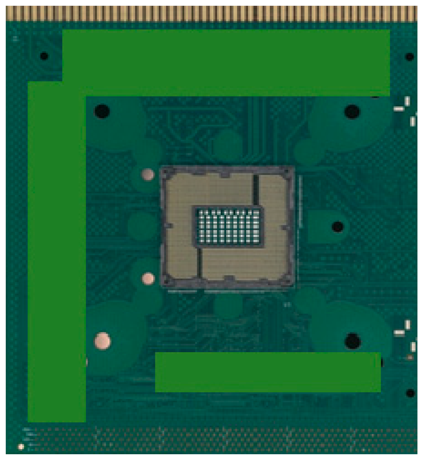
2.1. TV Description
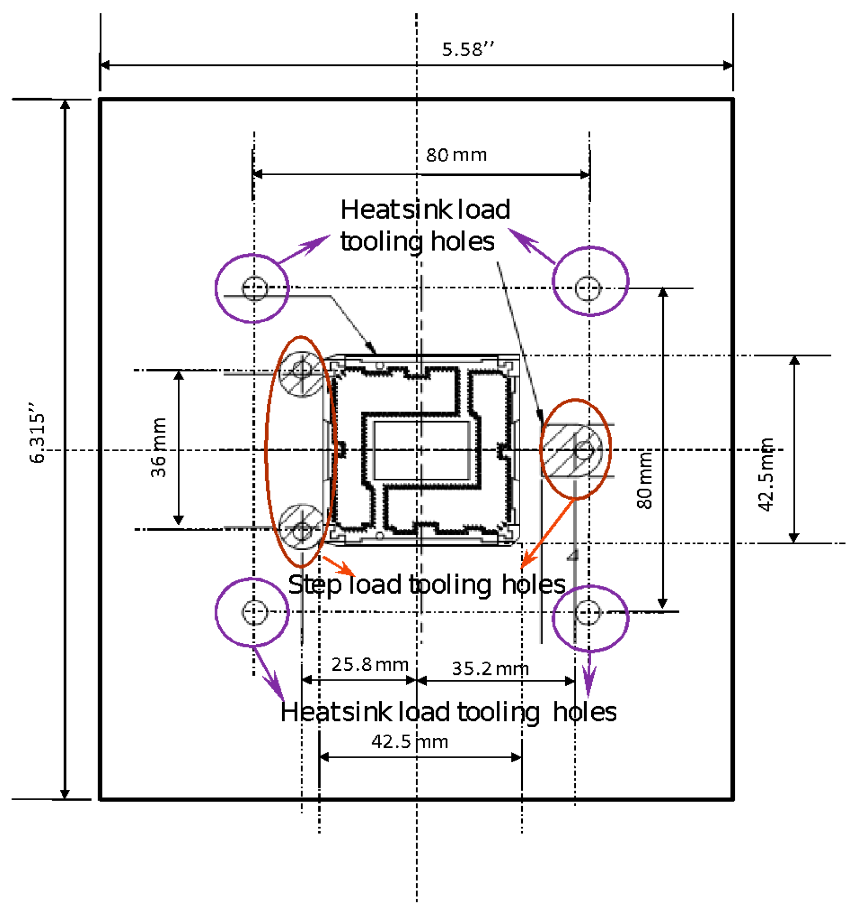
TV of Ibex peak motherboard: The enabling test board (ETB) was designed to simulate the performance of the Ibex peak motherboard in order to be used in an in-circuit test (ICT), and to evaluate the interface land grid array (LGA) socket’s electrical, mechanical, and reliability performance. The nominal dimension of the ETB and interface socket was 6.315 inches × 5.58 inches and 42.5 mm × 42.5 mm, respectively. There were two sets of tooling holes: One set with three tooling holes was designed to simulate the load applied to the substrate steps, and the other set with four tooling holes was to simulate the heat sink load. The schematic representation and picture of ETB are shown in
Figure 1 and
Figure 2, respectively.
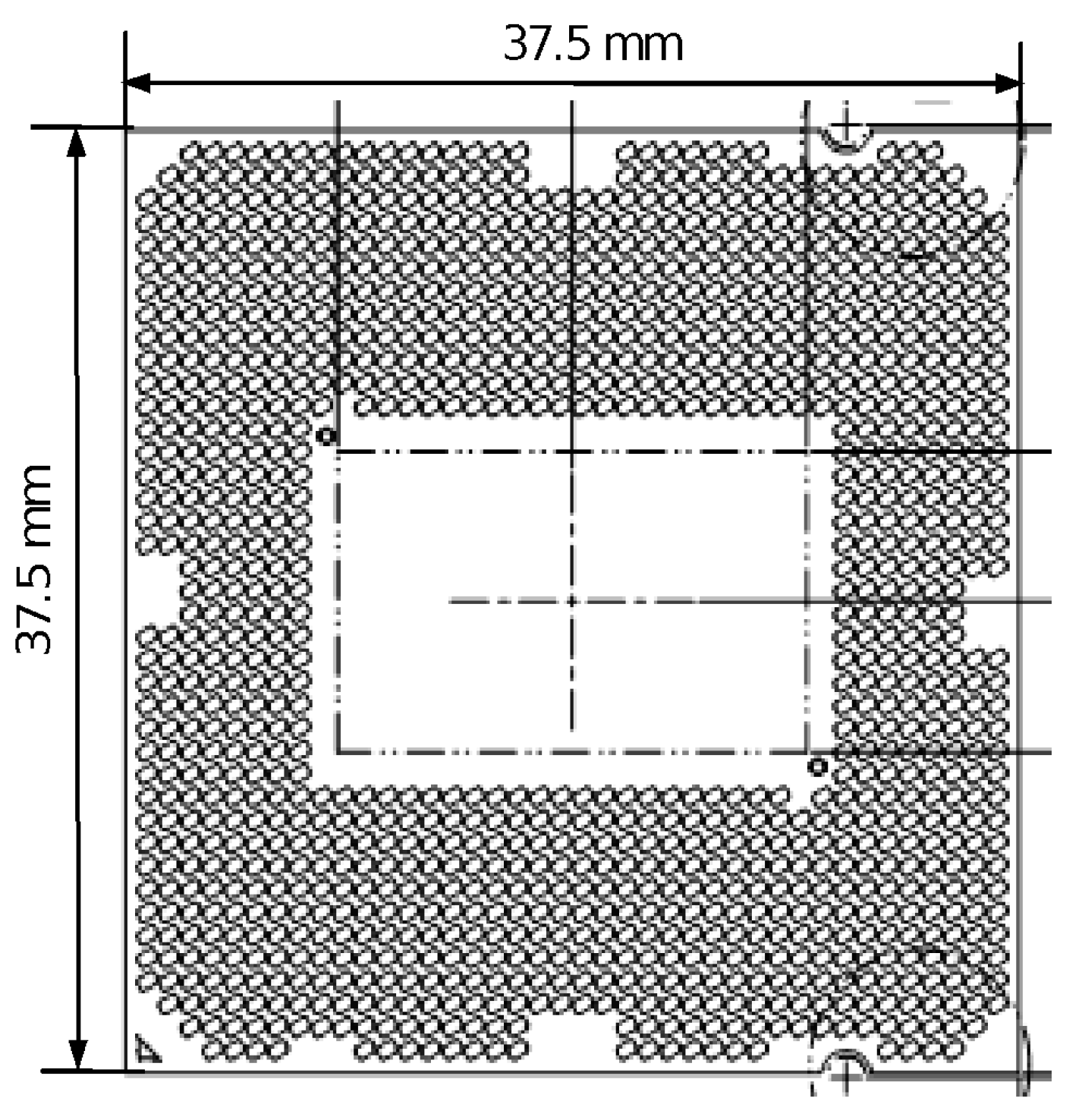
TV of Clarkdale processor package: The nominal dimension of the substrate size was 37.5 mm × 37.5 mm, as shown in
Figure 3. There were two-step loads that were applied to the ears of integrated heat spreader (IHS). There was a heat sink (HS) load on the top surface of the IHS. The loads on the IHS are shown in
Figure 4.
2.2. Measurement of LLCR
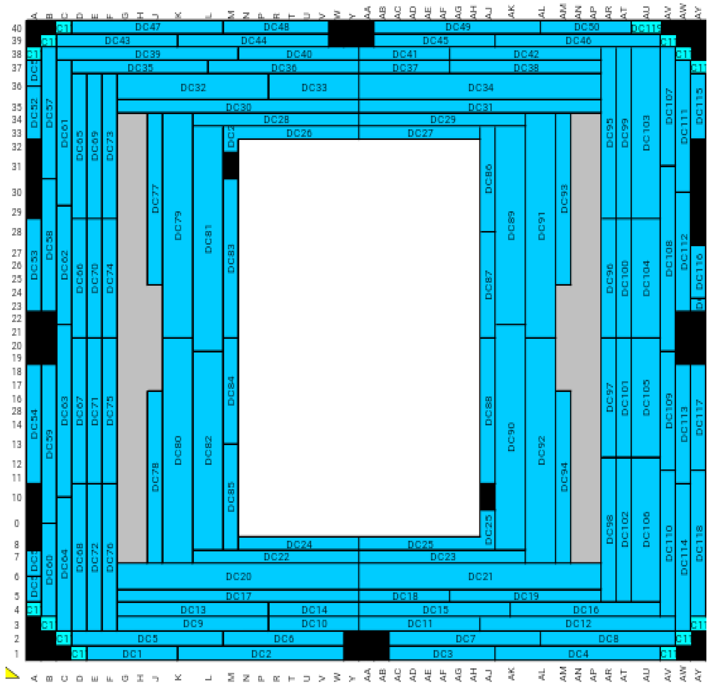
Daisy chain layout: The pattern was designed by following these strategies: (a) The whole array shall be divided into small chains to get reasonably accurate measurement; (b) the high risk of shorting shall be caught; and (c) the high risk of opening or high resistance shall be caught. There were 119 chains in total. The schematic representation of the daisy chain layout is shown in
Figure 5.
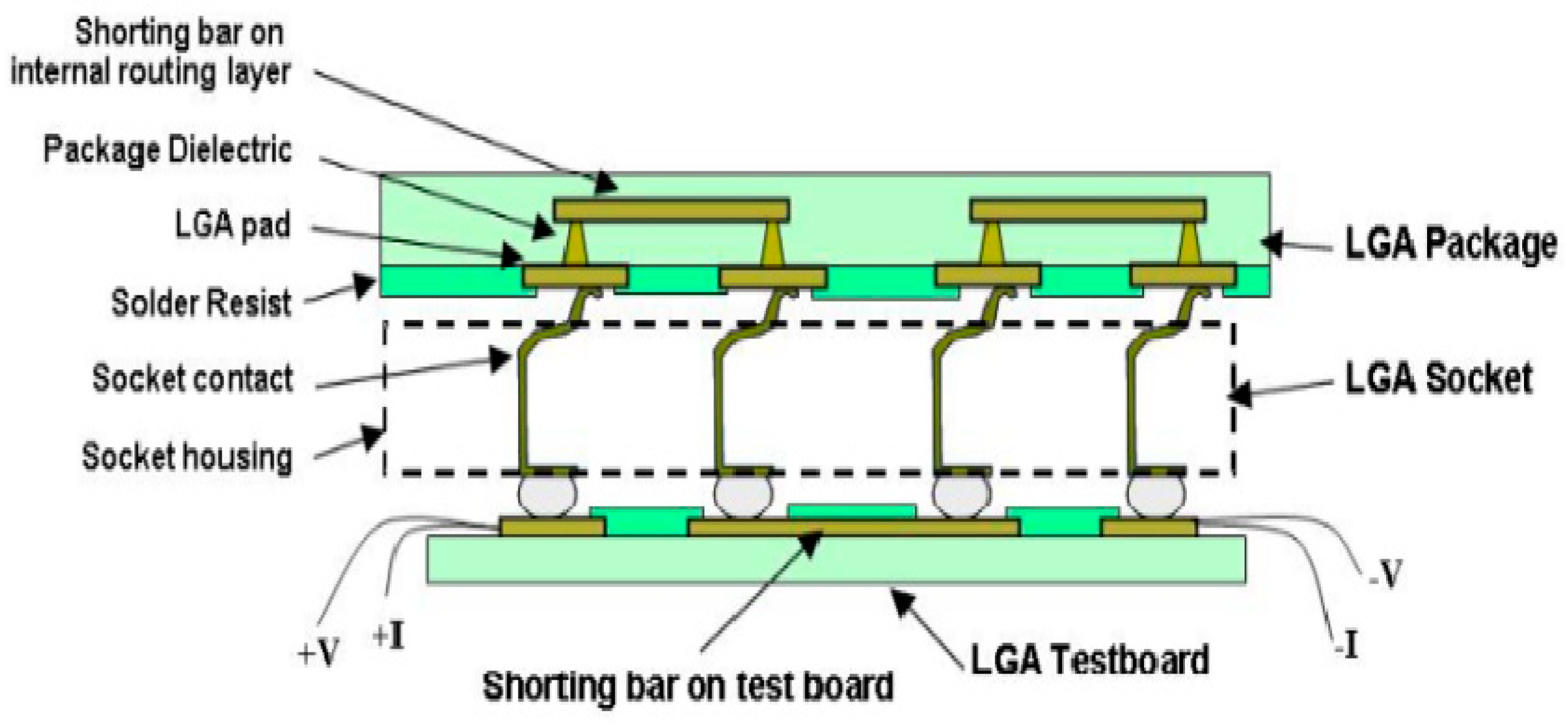
The four-wire measurement technique was adopted: The electrical measurement instrument provided two separate circuits. One was a precision current source to deliver the test current. The other was a precision voltmeter circuit to measure the voltage drop between the desired points. Thus, the total resistance was able to be calculated based on the measured current and voltage from each chain. The total resistance per chain (
) measured thus included the resistance of package and package shorting bars, contact LLCRs, solder balls, and motherboard and motherboard shorting bars, as shown in
Figure 6.
Parasitic resistance: LGA TVs were flush-mounted directly to the motherboard fixtures in oreer to measure the average parasitic resistance (), which included the resistance of the package, the motherboard, and solder balls. Thirty samples were used for statistical reasons.
The value of low-level contact resistance
can be calculated by:
where
is the number of contacts within the chain.
3. Test Details
3.1. Enabling Load TH Test Legs
3.1.1. Risk Assessment
As part of the validation process, in order to understand if the product would remain in good function until its guarantee period, a bunch of accelerated tests were performed, among which accelerated TH tests, typically testing at 85 °C/85% relative humidity, were adopted to simulate the system performance in hot and humid environments. Such TH tests could either be tested until failure to understand the products’ capability or be tested until the equivalent warrantee time requirement
. The
in this paper was chosen as 408 h, based on the calculations using Peck’s acceleration model [
1].
TH tests were conducted at two extreme load ends. One was conducted under minimum external load, correlating with the risk of insufficient contact force to penetrate through the foreign material that may form during the product life. The other one was conducted under maximum external load, correlating with the risk of contact wiping all the way to the solder resist opening (SRO), which was due to the interaction with SRO, resulting in the reduction of contact force and still ending up with insufficient contact force to penetrate through the foreign material that may form during the product life.
3.1.2. DOE Description
Leg1: The leg with max external load was labeled as leg1 and was tested under 135 lb step load with 50 lb HS load based on the design guide.
Leg2: The leg with min external load was labeled as leg2 and was tested under 60 lb step load.
Twelve units were tested for each leg.
3.1.3. Success Criterion
The average part resistance per design
(hereinafter referred to as part average resistance) was required to be less than 19 milliohms per design guide, as shown in Equation (2).
The maximum allowable chain LLCR resistance
(hereinafter referred to as max chain LLCR limit) was defined by assuming that only one contact reaches a maximum of 100 milliohms, while the rest of the contacts within this chain all meet the part average requirement. Thus, the
requirement per chain could be calculated by Equation (3) and is dependent on the number of contacts within the chain, as shown in
Table 1.
3.1.4. Enabling Load TH Test Results
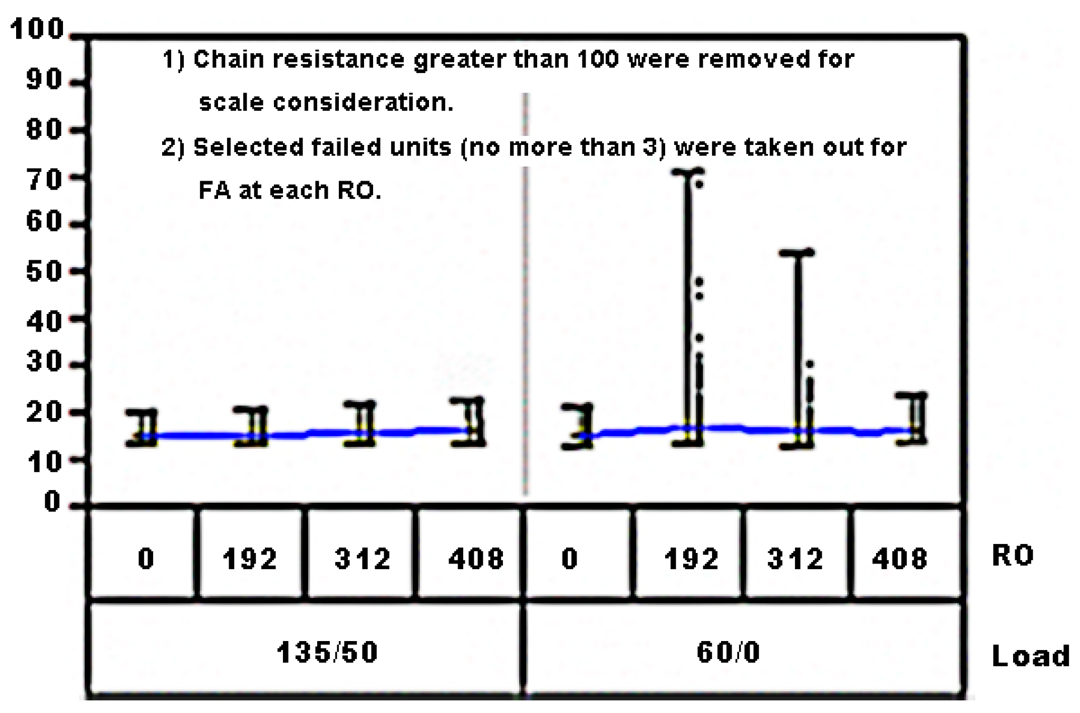
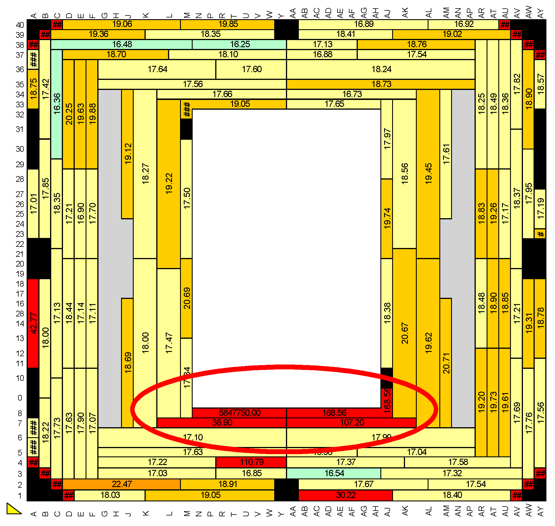
The data of
for the tested units were collected at three different readouts (RO), 192 h, 312 h, and 408 h. They were plotted in the variability chart below, together with
at time zero (before units being put into chamber), as shown in
Figure 7. In the chart, the resistances greater than 100 milliohms were not plotted for scale consideration. It can be seen that the TH tests under high load was good; the TH tests at time zero were good; but for the TH tests under min load, there were many failures. Additionally, note that at each RO, failed units (no more than three) were taken out for failure analysis (FA). These failed units did not go back to chamber to next ROs. This is why the resistances appear to get better with time for the min load case (since some failed units were taken out).
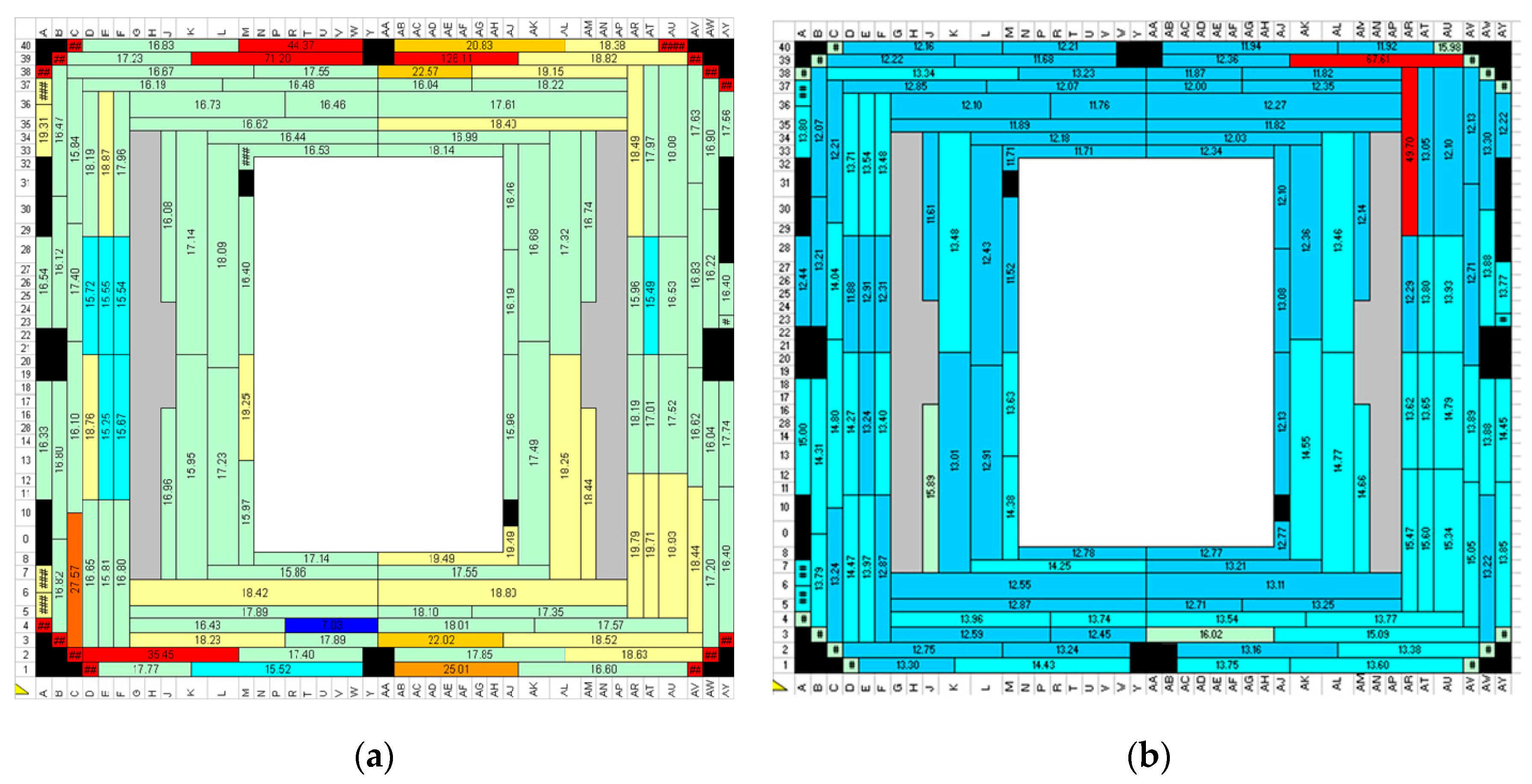
The measured LLCRs were plotted against the daisy chain layout (as illustrated in
Figure 5) for each unit and at each RO.
Figure 8 below shows two selected
maps. The selected maps were from the units at 192 h RO under min load leg. These two units were taken out for FA due to failures.
The LLCR map of a unit from another TH leg is shown in
Figure 9. The test setup for this leg was the same as the previous min load leg, but the socket supplier was different. This unit was not used for any comparison in this paper, but only to demonstrate that this TH failure could happen at the inner perimeter and could exhibit as an open failure.
From the LLCR distribution, it can be seen that there was no obvious pattern in terms of the failure location distribution. With step load on the North and South sides, the contact force distribution map is shown in
Figure 10 (Note: NFORC3 divided by 10,000 is in gram force). With the package warped upwards in the center, the contact force had a tendency to decrease from the exterior perimeter to the interior perimeter, whereas the failures were found both around the outer perimeter and the inner perimeter. These were typical TH failure symptoms.
3.1.5. Failure Analysis and Root Cause Failure
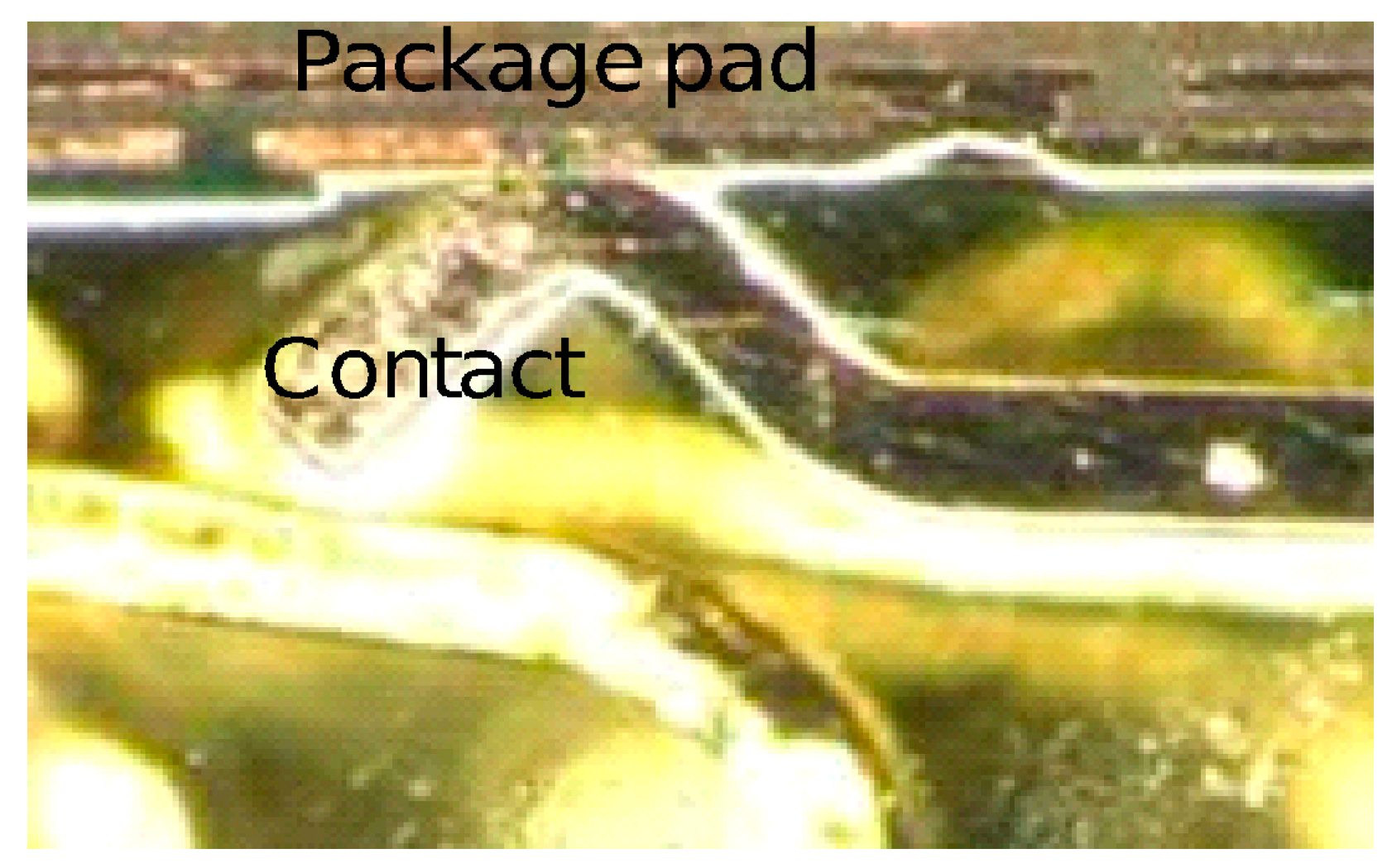
X-sections showed that all contacts remained on pads (even for the open failure chain), as shown in
Figure 11. Scanning electron microscope (SEM) showed that, for the pad from failing chains, there was the presence of nickel oxides. For functional chains, there were mostly no signs of other elements besides Au, as shown in
Figure 12. Even during the appearance of other elements for good chains, the contact forces were believed to be strong enough to penetrate through the foreign materials in order to make good contact with the pads.
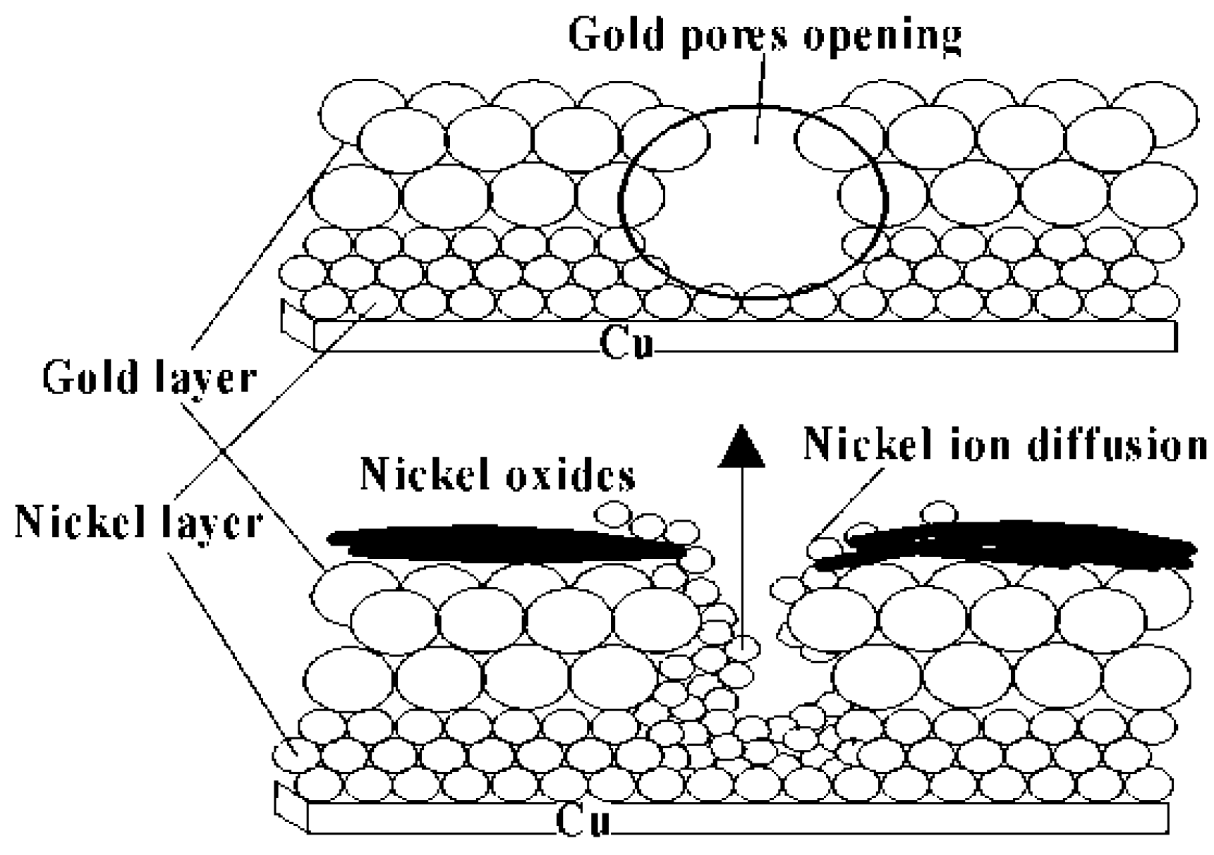
TH FM: The metallurgical surface finish for the package and the contacts was typically electroless nickel and immersion gold plating (ENIG). A typical industry process for ENIG [
2] is such that the immersion gold (IG) is deposited on top of electroless Ni (EN), which is on top of the Cu layer. EN serves as a diffusion barrier for copper metallization, whereas IG acts as a protective overcoat to protect Ni from oxidation. Since a gold atom is much larger than a nickel atom, the room between nickel atoms may not be fully filled in by gold atoms, thus small voids are formed during the displacement reaction. The presence of gold pores exposed the nickel underneath, and under high relative humidity environment, diffusion brings nickel ions to the surface, resulting in the formation of nickel oxidation, as shown in
Figure 13. At time zero, it was expected that even though the entire contact surface was not all gas tight, the contacting spots could be considered gas tight [
3]. Therefore, good LLCR was always established at T0. With time passing, corrosion was accelerated under high relative humidity and stress relaxation occurred. The mating locations could change due to stress relaxation, and this was how corrosion products got between the original contacting spots. In hot humid environments, the high temperature also adversely impacted electrical performance. It not only sped up corrosion, but also caused more severe stress relaxation. In extreme severity, oxidation in TH could lead to electrical failures, such as high resistances or electrical opens.
Note that, besides the nickel oxidation type of corrosion, there were some other commonly seen TH FMs, such as fretting, that caused the wear of the coating material on the contact surface, then exposed the EN layer, or even exposed the base material of the Cu layer, resulting in the decrease of the electrical contact performance, such as wiping, dust, industrial corrosive gases, etc.
3.2. Some Main Modulators of TH FM on Electrical Contact
3.2.1. Main Modulators
Based on the TH FM, several main modulators that are believed to have great impacts on TH performance, and can be implemented through relatively non-complicated design applications, were identified. They were:
Enabling load: The theory is that the possibility of contacting points penetrating through the films/the foreign materials is a function of contact force. Increasing contact force increases the possibility of forming air tight contacting points. Thus, the solution was to increase the enabling load.
Surface finish thickness: The theory is that increasing the IG plating thickness helps reduce the number of the pores, and thus mitigate the formation of nickel oxidation in order to improve the resistance to TH. The solution was to increase the Au thickness.
Contacting area: The theory is that increasing contacting area helps improve the contacting efficiency, since larger contacting areas may provide more space for more gas tight contacting points. Note: The larger the contacting area, the smaller the contact pressure. Thus, in order for the contacting area to play a positive role, a minimum contact force was required. The solution was to increase the contacting area with the minimum contact force requirement being met.
The first proposed solution of increasing the enabling load and the second proposed solution of increasing Au plating thickness were more straightforward, but the third one of increasing contacting area was tricky. It had to do with the detailed design of a contact tip. Additionally, the nominal contacting area was not equal to the actual contacting area since not all points within the nominal area were gas tight. It has been a challenge to investigate these gas tight points. There are some papers on this topic. The single-spot first-order model for constriction resistance established by Holm [
4] has received international recognition. On the basis of this model, many researchers have studied the influence of many factors such as multi-contact spot, temperature, arc, film, time, etc. A variety of complex theoretical models of contact resistance have been established. Malucci simulated the contact performance by considering the combined effects of surface degradation and interface motion on the change of contact resistance, and proposed a third level multi-spot constriction model [
5,
6]. Han and Kim studied the effect of normal forces on fretting corrosion in tin-coated electrical contacts, and found that there is a linear relationship between the normal forces and the threshold displacement amplitude [
7]. Park and Lee developed an empirical equation to account for the impact of fretting frequency or temperature, and proposed failure-time variation sensitivity for each variable [
8]. However, very few studied how to quantifiably correlate the tip design with contact electrical performance. This paper proposed a new methodology to correlate contact tip design with contact resistance.
3.2.2. The Model to Correlate Contact Tip Design with Contact Resistance
Key Parameters
Regarding contact tip design, there were two key parameters identified: Contact tip radius
and contacting width
, as shown in
Figure 14. They are critical to function tip design dimensions that are directly related to contacting area. In this paper, for the simplicity of study, the focus was on the influence of
.
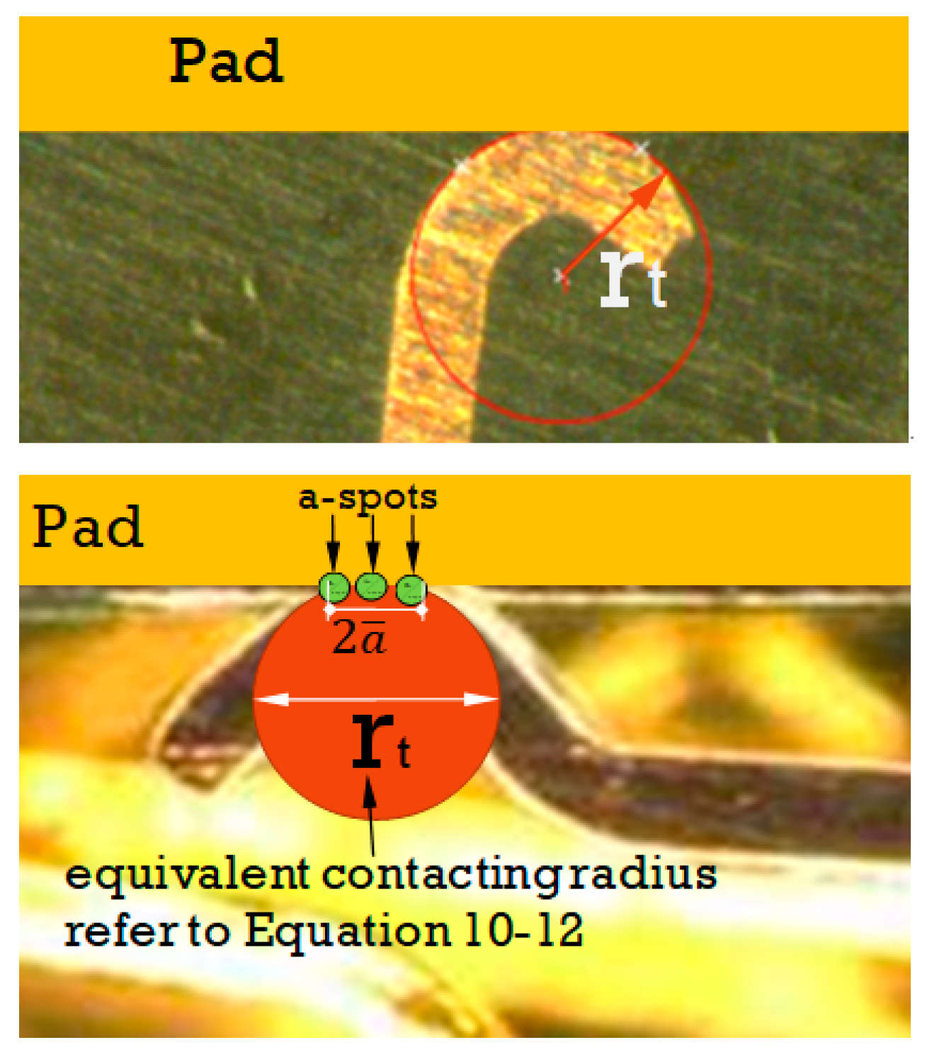
Asperity Spots
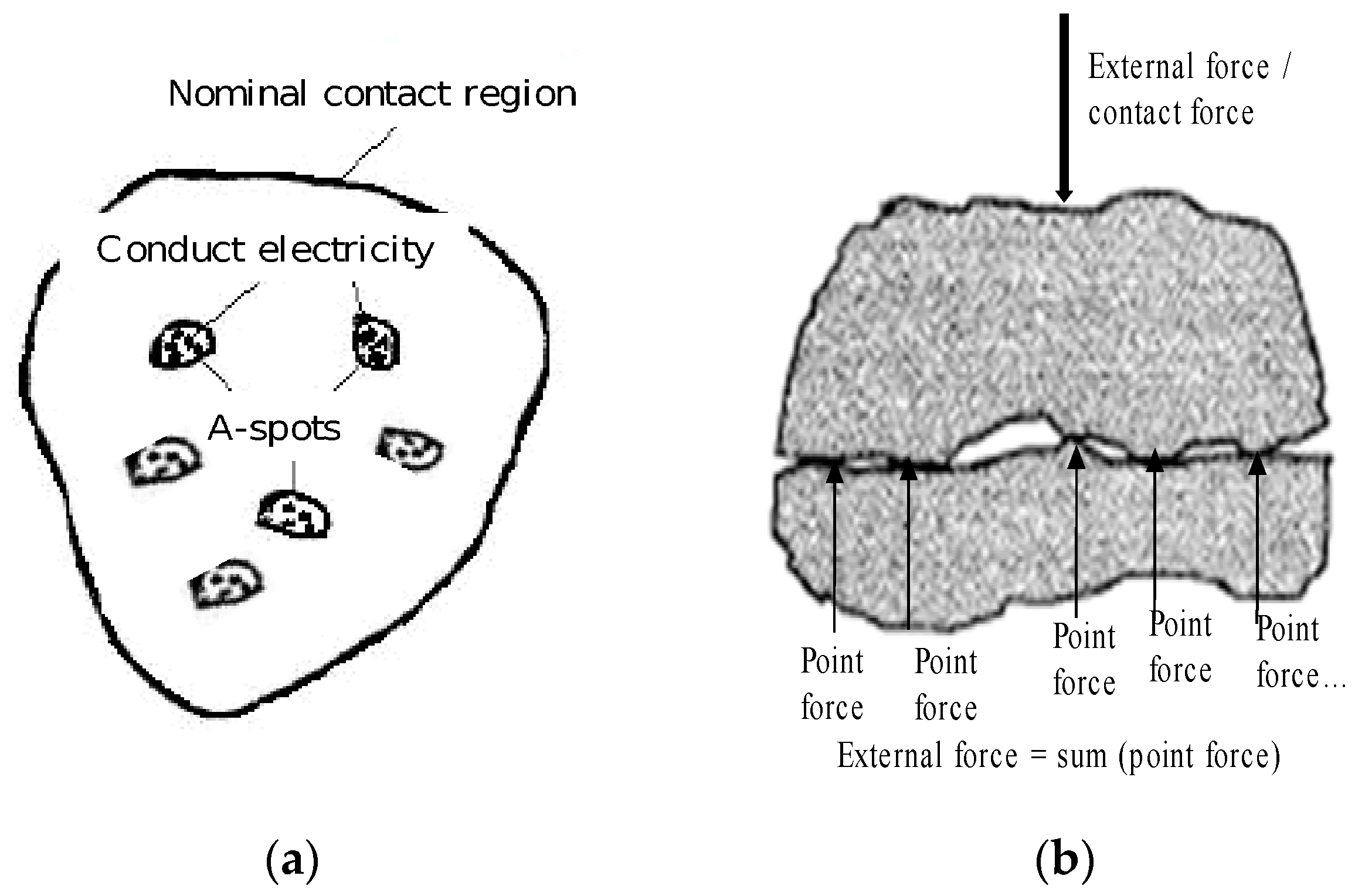
The contacting interfaces of two conductors, no matter how well the surface was processed, were always uneven on the micro level. If the hardness of the material was infinite, the contact force does not cause any deformation. There will be, at most, three contact spots for surface-to-surface contact; two contact spots for line to surface contact; and one contact spot for sphere to surface contact. However, in reality, the material will deform. Thus, the number of contact spots will increase with the increase of the deformation, until the summation of the forces provided by point contacts is balanced by the external force, and the increase of contact spots stops, as shown in
Figure 15. These spots, which actually touch, are called asperity spots (hereinafter referred to as a-spots), and are the ones that can actually conduct electricity.
Assumptions
As illustrated in
Figure 16, the tip along the contact length direction was viewed as a spherical ball with a radius of
and with all a-spots on top of it.
The pad was viewed as an ideal spherical surface with an infinite radius of curvature or an ideal plane.
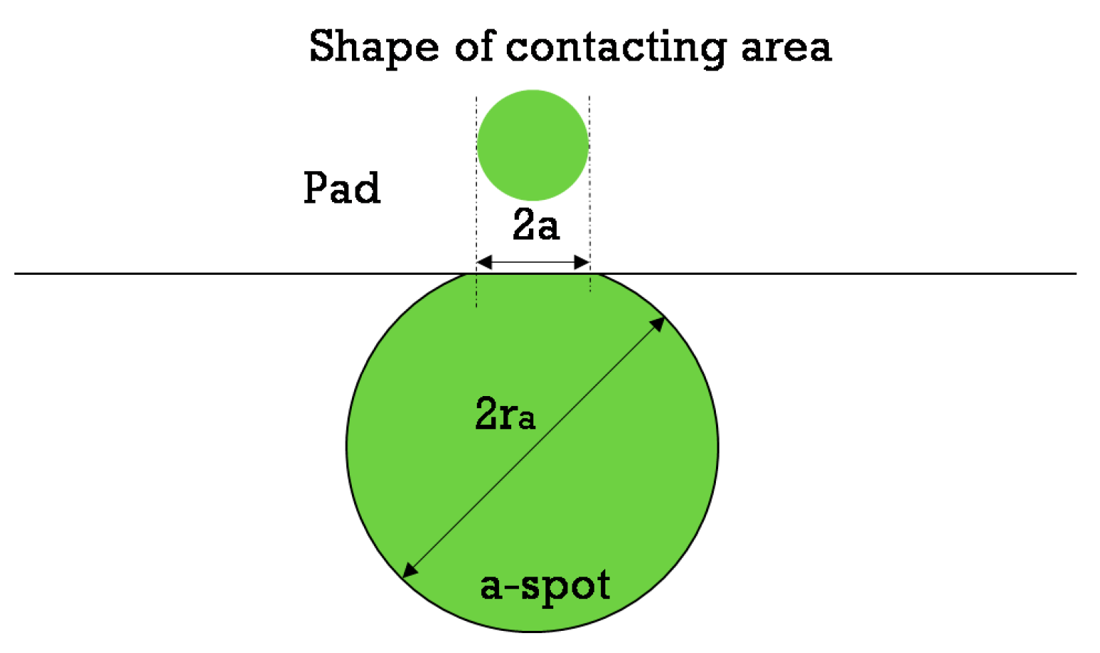
The a-spots were treated as a bunch of small balls, all with a radius of (hereinafter referred to as a-spot ball radius).
The contacting interface of an a-spot was a circle, with a radius of
(hereinafter referred to as a-spot contacting radius), as shown in
Figure 17.
When the touch just began, there was only one a-spot touching pad. As the actual contacting area was small, the force on the contact point was large, resulting in deforming the 1st a-spot. With the increasing deformation of the 1st a-spot, the 2nd a-spot started touching the pad. Assuming that, when the 2nd a-spot came into play, the 1sta-spot was still in elastic region. Thus, the classical Hertz formula could be used to calculate the elastic deformation. Additionally, this procedure was repeated for all other a-spots until the supporting forces from a-spots could balance the external force.
The number of a-spots was n, and the distance between a-spots was much greater than a-spot contacting radius , and therefore any interference from the adjacent a-spots could be ignored.
As a result, the a-spot contacting radius could be derived with the classic Hertz Formula [
9], which was expressed as:
is the contact force on an a-spot;
is a-spot ball radius; and
,
,
,
E2, are Poisson’s ratio and Young’s modulus of the two conductor materials, respectively. As both contacting surfaces were Au plated, we have:
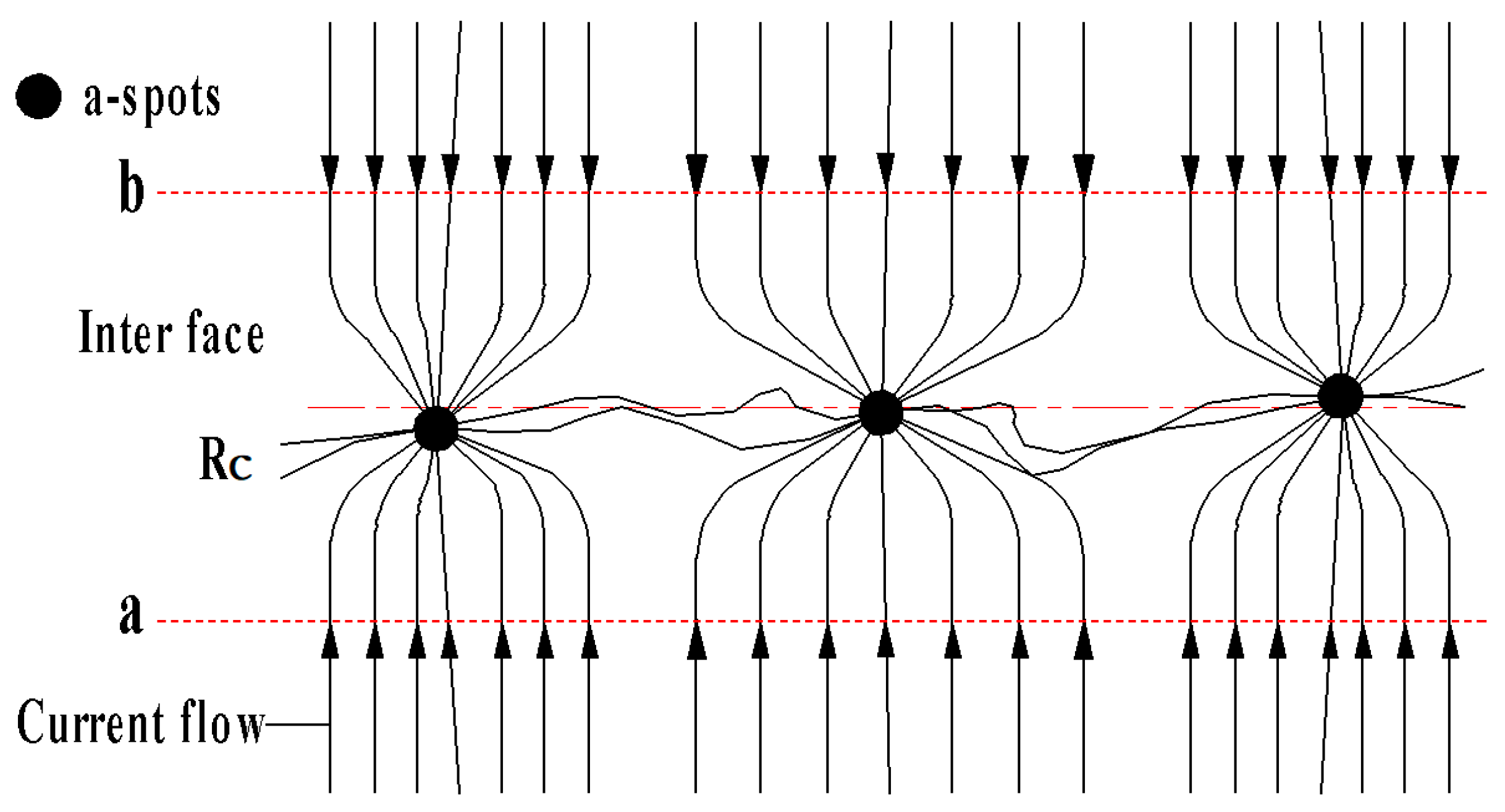
LLCR
As the actual contact interface was a group of a-spots, resistance increased as the path of current flow was elongated when current passes through a-spots. Such resistance was defined as constriction resistance
, as depicted in
Figure 18.
For the round contacting interface, there was the following relationship:
is the constriction resistance of an a-spot (hereinafter referred to as a-spot constriction resistance); is a-spot contacting radius; and is resistivity of the contacting material, which is also the resistivity of Au.
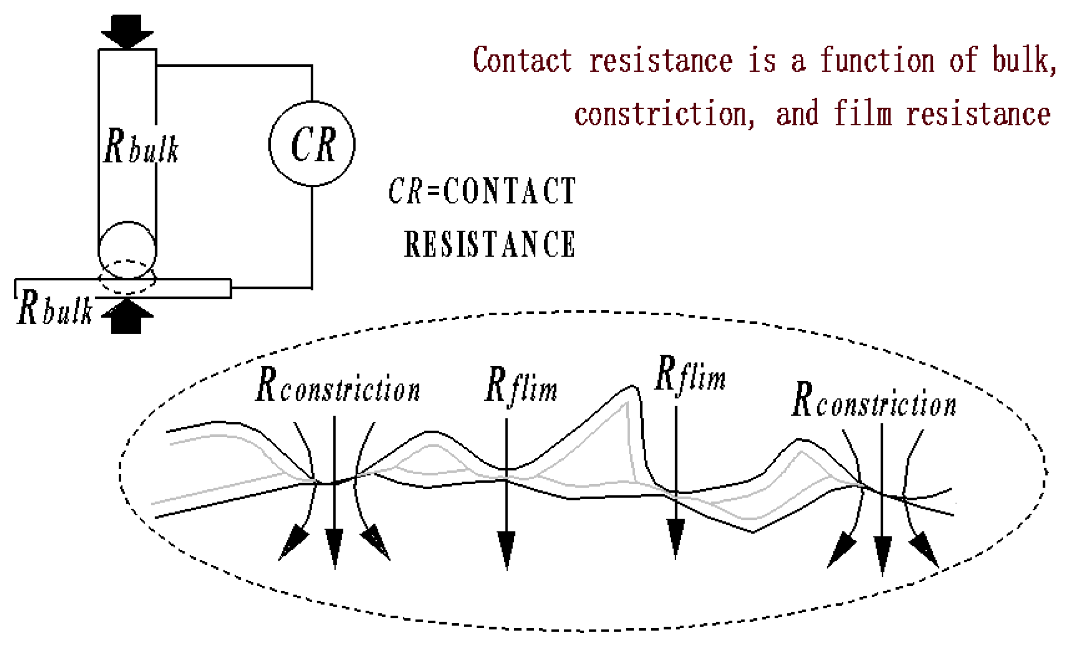
Contact resistance consists of bulk resistance, constriction resistance, and film resistance, as shown in
Figure 19. A-spot constriction resistances
are in parallel at the interface. Thus:
is the total constriction resistance at the interface (hereinafter referred to as interface constriction resistance). Assuming that film resistance is infinite and its conductive effect could be ignored, then represented the resistance of the interface.
Assuming there were
n a-spots in total, Equations (10)–(12) could be:
is the total true contacting area; is the contacting radius of a single point contact with equivalent contacting area of (hereinafter referred to as equivalent contacting radius); and is the constriction resistance of a single point contact with equivalent contacting area of (hereinafter referred to as equivalent constriction resistance).
was in series with the bulk resistance of the contact
and the bulk resistance of the pad
. Thus:
is the total single contact resistance from single contact measurement. When deducting the bulk resistance of the pad, we got LLCR because the pad resistance was a portion of the parasitic resistance, as illustrated in
Section 2.2. Thus:
Contact Tip Radius Design
In order to connect the contact tip design with LLCR, the tip radius
was chosen to be the same as the radius of the single point contact (hereinafter also referred to as equivalent ball radius) that created equivalent constriction resistance
. The following relationship was thus established:
is the total contact force. In this paper, the minimum required contact force of 15 gramforce, based on design guide was chosen. is a-spot constriction resistance; is the total number of a-spots; is the resistivity of Au; and is Young’s modulus of Au.
Design criterion: For a conservative design, no contact resistance was allowed to exceed the requirement of average part resistance
.
Besides, to account for the impact from factors not considered in this paper, such as the influence of surrounding a-spots, the influence of the deviations of assumptions from real situations, etc., a safety coefficient of
was assumed.
Bulk resistance of contact
was dependent on the contact design. However, once the big picture of a contact was determined,
was pretty much settled. Minor modifications on a tip design did not have much effect on its value. In this case,
was rounded up to 9 milliohms per design guides. Thus, there is the following relationship.
In hot and humid environments, nickel oxides or other foreign materials develop and can cover the a-spots, making a-spots lose their good electrical conductivity. As more and more a-spots are covered by foreign materials, the interface constriction resistance and LLCR keeps increasing, leading to high resistances or open failures in severe cases. Assuming that only one good a-spot was left, the following relationship was observed:
The resistivity of Au was taken as
. The Young modulus of Au was taken as 790 Mpa. Thus:
For different values of
, a requirement of a-spot ball radius
could be obtained. From
, a-spot contacting radius
could be derived, then a-spot constriction resistance
could be derived, then equivalent constriction resistance
could be derived, and then contact tip radius
(also referred to as equivalent ball radius) could be derived. Therefore, for a given
, a minimum design requirement of contact tip radius could be calculated, based on the requirements of LLCR. This minimum tip radius design requirement was called
. The maximum tip radius requirement came from the contact wiping tolerance analysis, which was not in the scope of discussion of this paper, and is just denoted with
. Therefore, the tip radius fell in the range of:
As far as n is concerned, it has to do with the surface finish technology, but a very small value and a large value are both not realistic. For a small n, say just one a-spot, once it is covered by foreign material, the contact will fail. For a large n, the a-spot force will be small and the ability to penetrate through foreign materials will be compromised. Additionally, it may require a large tip that exceeds .
As illustrated in
Table 2, the recommended design of tip radius
was determined. A value smaller than the recommended
was no good; a value larger than the recommended
may have reasonable risk controls. For example, if there are 10 a-spots:
; if there are 15 a-spots:
; and if there are 20 a-spots:
.
3.3. TH DOEs of Modulating Factors
3.3.1. TH DOEs
From Leg1 and Leg2 described previously, it can be seen that increasing the enabling load can be a solution since, even though the min load leg (leg2) failed, the high load leg (leg1) passed.
The focus of this portion was on studying the second main modulator (surface finish thickness) and the third main modulator (contacting area). Note: The contacting area was calculated as .
Leg 3: Smaller nominal contacting area leg with thinner Au thickness. The change in contacting area was reflected on the contact side by purposely designing a smaller contact tip. The contacting area was 0.007 mm2. The Au thickness was controlled on the package side. The average pad Au thickness was 0.38 µm.
Leg 4: Larger nominal contacting area leg with thinner Au thickness. The change in contacting area was reflected on the contact side by purposely designing a larger contact tip. The contacting area was 0.0221 mm2. The Au thickness was controlled on the package side. The average pad Au thickness was 0.38 µm.
Leg 5: Larger nominal contacting area leg with thicker Au thickness. The change in contacting area was reflected on the contact side by purposely designing a larger contact tip. The contacting area was 0.0221 mm2. The Au thickness was controlled on the package side. The average pad Au thickness was 0.43 µm.
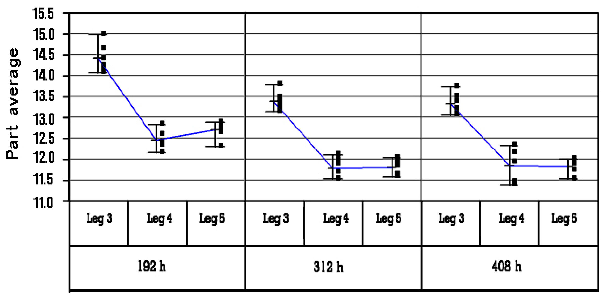
3.3.2. Test Results
Here,
was used for analyses to get rid of the uncertainty caused by LLCR variation. Since it is typical that under TH, chain LLCR maps do not have an obvious pattern. Thus, only analyses based on part average resistance could tell if the improvement is a random kick in or a true stable help. Three ROs were collected at 192 h, 312 h, and 408 h. They were plotted in the variability chart, as shown in
Figure 20. It can be seen from the comparison of leg3 vs. leg4 and leg3 vs. leg 5 that the part average was constantly improved by about 1.5 milliohms to 2 milliohms. If compared with the design requirement of
of 19 milliohms, the improvement was about 7.9%–10.5%. There were more tests conducted to confirm the improvement by implementing the proposed design, even though they were not described in this paper, the improvement on part average resistance always held.
There is not much difference between leg 4 and leg5. The increase in Au thickness seems to make a negligible difference. It is believed that it is because the typical industrial plating process is reasonably mature already.
Besides, it is noticeable from
Figure 20 that the resistance, in general, appears to get slightly better with time, especially from 192 h RO to 312 h RO. The author’s suspect that this is due to the system creep and contact relaxation that result in contact force redistribution and contacting status readjustment. Additionally, typically creep and relaxation happen faster within the early stage, which may explain why the drop in resistance is more obvious from 192 h RO to 312 h RO. More study is needed in future work to further investigate this phenomenon.
3.4. Solutions
From the previous experiments and the theoretical analyses, it is believed that both the enabling load and contacting area play important roles in improving the electrical performance under TH for area array packages/printed circuit board interfaces. To get better TH performance, increasing the enabling load helps, and increasing the contacting area (with a minimum contact force requirement being met) also helps.
There are relationships between metallurgical surface finish and key tip design parameters. Larger contacting areas are able to provide more space for more gas tight contacting points. When the contact force meets the minimum requirement, increasing contacting area actually helps improve the contacting efficiency by giving full play to the potential of metallurgical surface finish. Additionally, with more gas tight contacting points, the possibility of all a-spots being covered by foreign materials under TH is less. This paper proposed a design optimization methodology to correlate tip radius with asperity spots and contact resistance requirements. The proposal proved to be efficient.
Increasing the enabling load is the typical industrial solution, but it leads to extra cost in loading mechanism design, and in printed circuit boards design, etc. For instance, in order to get to higher load, a thicker backing plate and/or a thicker loading plate is needed. The extra material to be used can result in huge costs when it comes to high volume manufacturing. Besides, with a higher enabling load, it is very likely that extra effort is needed to accommodate for the risk due to creep on the maximum load end. More seating plane areas may be needed. This can result in less pin count, and needless to say, it is not desirable.
Thus, in industrial application, the design strategy proposed in this paper shall be a reasonable first step to take in order to optimize the electrical performance under TH and to save cost. If this route is insufficient, other solutions such as increasing the enabling load may come in as a second step.
4. Conclusions
A methodology that correlates asperity spots and contact tip design with contact resistance is proposed and proved to significantly improve the electrical performance for area array packages/printed circuit boards interfaces. With such a design implemented, a reduction in part average resistance of 1.5 milliohms to 2 milliohms, or an improvement of 7.9%–10.5% (in comparison with requirement), has been seen in the Clarkdale and Ibex peak platform.
Both increasing contacting area and increasing enabling load proved to be able to effectively improve the electrical performance under hot and humid environments, but increasing Au thickness does not seem to help much. Increasing the enabling load is a typical solution, but it is costly. Increasing contacting area with the proposed methodology is a cost-effective solution and is a reasonable first step to take in industrial practice.
5. Future Work
It is interesting to observe a decrease in resistance with time in general, and the drop is more obvious in the early stage. The authors suspect the observation has to do with system creep and contact relaxation [
10]. These will be investigated in the future.
Besides, microprocessors are known with consuming huge power that can lead to local hot spots. These hot spots are formed due to high current flow and poor contacts [
11]. Hot and humid environment will have an adverse effect on contacting quality. Poor contacts, in turn, lead to more local hot spots and to a higher probability of physical failures. Thus, adding the impact of power consumption and heat dissipation into the study shall be a very critical and interesting topic as well.
Furthermore, the design criterion for tip width has not been established. This will be illustrated in future work.
Some other factors such as the influence of wiping and fretting are also worth looking into [
12].
Author Contributions
Conceptualization, Y.L.; methodology, Y.L.; software, Y.L. and Z.G.; validation, Y.L., W.M., H.S., Z.G., G.L. and B.W.; formal analysis, Y.L. and W.M.; investigation, Y.L. and W.M.; resources, Y.L.; data curation, Y.L. and W.M.; writing—original draft preparation, Y.L. and W.M.; writing—review and editing, Y.L., W.M., K.Z., G.L. and B.W.; visualization, Y.L.; supervision, Y.L.; project administration, Y.L.; funding acquisition, Y.L. and K.Z.
Funding
This research was funded by Key Research and Development Plan of Liaoning Province (No. 2019JH2/10100014), National Key R&D Plan (No. 2017YFC0703903), and National Science Foundation of China (No. 51705341, 51675353).
Acknowledgments
The research has been supported by Overseas Expertise Introduction Project for Discipline Innovation No. D18017, and by Intel Corporation, Karumbu Meyyappan, Russell Aoki, et.al. Special thanks are given for making this research possible.
Conflicts of Interest
The authors declare no conflict of interest. The funders had no role in the design of the study; in the collection, analyses, or interpretation of data; in the writing of the manuscript, or in the decision to publish the results.
References
- Peck, D.S. Comprehensive Model for Humidity Testing Correlation. In Proceedings of the 24th IEEE International Reliability Physics Symposium, Anaheim, CA, USA, 1–3 April 1986. [Google Scholar]
- Johal, K.; Brewer, J. Are you in control of your Electroless Nickel/Immersion Gold process? In Proceedings of the IPC Works 2000, Miami, FL, USA, 9–14 September 2000. [Google Scholar]
- Meng, C.K.; Selvamuniandy, T.S.; Gurumurthy, C. Discoloration related failure mechanism and its root cause in Electroless Nickel Immersion Gold (ENIG) Pad metallurgical surface finish. In Proceedings of the 11th International Symposium on the Physical and Failure Analysis of Integrated Circuits IPFA 2004, Taiwan, Taiwan, 5–9 August 2004. [Google Scholar]
- Holm, R. Electric Contacts, 4th ed.; Springer: Heidelberg, Germany, 1967; pp. 82–108. [Google Scholar]
- Malucci, R.D. Multispot model of contacts based on surface features. In Proceedings of the Thirty-Sixth IEEE Holm Conference on Electrical Contacts, Montreal, QC, Canada, 20–24 August 1990. [Google Scholar]
- Malucci, R.D. Dynamic model of stationary contacts based on random variations of surface features. IEEE Trans. Compon., Hybrids, Manuf., Technol. 1992, 15, 339–347. [Google Scholar] [CrossRef]
- Han, D.W.; Kim, H.Y. Effect of normal forces on fretting corrosion of tin-coated electrical contacts. Microelectron. Reliab. 2017, 79, 321–327. [Google Scholar] [CrossRef]
- Park, Y.W.; Lee, K.Y. Development of empirical equations for fretting-corrosion failure-time of tin-plated contacts. Wear 2008, 265, 756–762. [Google Scholar] [CrossRef]
- Hertz, H. On the contact of elastic solids. J. für die Reine Angew. Math. 1880, 92, 156–171. [Google Scholar]
- Demidov, A.V.; Makarov, A.G.; Pereborova, N.V.; Egorova, M.A. Variants of mathematical simulation and systems analysis of mechanical relaxation and creep of polymer materials. Fibre Chem. 2018, 5, 1–6. [Google Scholar] [CrossRef]
- Al-Hashimi, M.; Saleh, M.; Abulnaja, O.; Aljabri, N. Evaluation of control loop statements power efficiency: An experimental study. In Proceedings of the 9th IEEE International Conference on Informatics & Systems, Cairo, Egypt, 15–17 December 2014. [Google Scholar]
- Kim, M.J.; Kim, H.K. Effects of temperature and span amplitude on fretting corrosion behavior of tin-plated electrical contacts. Microelectron. Reliab. 2017, 69, 80–87. [Google Scholar] [CrossRef]
Figure 1.
Schematic representation.
Figure 1.
Schematic representation.
Figure 2.
Enabling Test Board.
Figure 2.
Enabling Test Board.
Figure 3.
Schematic representation of the substrate size.
Figure 3.
Schematic representation of the substrate size.
Figure 4.
Load on integrated beat spreader.
Figure 4.
Load on integrated beat spreader.
Figure 5.
Schematic representation of daisy chain layout.
Figure 5.
Schematic representation of daisy chain layout.
Figure 6.
Schematic representation of the four-wire measurement technique. LGA: Land grid array.
Figure 6.
Schematic representation of the four-wire measurement technique. LGA: Land grid array.
Figure 7.
Variability chart for low-level contact resistance.
Figure 7.
Variability chart for low-level contact resistance.
Figure 8.
Selected map of failing units. (a) Failing unit No 1; (b) failing unit No 2.
Figure 8.
Selected map of failing units. (a) Failing unit No 1; (b) failing unit No 2.
Figure 9.
Example of temperature-humidity (TH) open failure.
Figure 9.
Example of temperature-humidity (TH) open failure.
Figure 10.
Contact force distribution under step load only.
Figure 10.
Contact force distribution under step load only.
Figure 11.
X-section of a failed chain.
Figure 11.
X-section of a failed chain.
Figure 12.
Scanning electron microscope (SEM)of pad from failing chain and good chain.
Figure 12.
Scanning electron microscope (SEM)of pad from failing chain and good chain.
Figure 13.
Schematic of the TH failure mechanism in electroless nickel and immersion gold plating (ENIG) surface finish.
Figure 13.
Schematic of the TH failure mechanism in electroless nickel and immersion gold plating (ENIG) surface finish.
Figure 14.
Contacting width and contact tip radius.
Figure 14.
Contacting width and contact tip radius.
Figure 15.
Real contact state. (a) Nominal contact region and conduct electricity spots; (b) Contacting status under equilibrium.
Figure 15.
Real contact state. (a) Nominal contact region and conduct electricity spots; (b) Contacting status under equilibrium.
Figure 16.
Schematic representation of a contact tip design.
Figure 16.
Schematic representation of a contact tip design.
Figure 17.
Schematic representation of contact state of an a-spot.
Figure 17.
Schematic representation of contact state of an a-spot.
Figure 18.
Schematic representation of constriction resistance.
Figure 18.
Schematic representation of constriction resistance.
Figure 19.
Schematic representation of contact resistance.
Figure 19.
Schematic representation of contact resistance.
Figure 20.
Variability chart for part average.
Figure 20.
Variability chart for part average.
Table 1.
per chain.
Table 1.
per chain.
| # of Contacts per Chain | Max Chain LLCR Limit |
|---|
| 2 | 59.50 |
| 4 | 39.25 |
| 6 | 32.50 |
| 8 | 29.12 |
| 10 | 27.10 |
| 12 | 25.75 |
| 14 | 24.78 |
Table 2.
Design parameters with different n.
(a)
| n = 1 | n = 10 |
|---|
| A-Spot Ball Radius ra (mm) ≥ | A-Spot Ball Radius ra (m) | A-Spot Contacting Radius a (m) | Resistance Rc = Rci = Rco (milliohm) | A-Spot Contacting Radius ai (m) | A-Spot Constriction Resistance Rci (milliohm) | Equivalent Constriction Resistance Rco (milliohm) | Interface Constriction Resistance Rc (milliohm) | Contact Tip Radius (Equivalent Ball Radius) rt min (mm) ≥ |
|---|
| 0.0020 | 2.016 × 10⁻⁶ | 1.679 × 10⁻⁶ | 7.000 | | | | | |
| 0.0202 | 2.016 × 10⁻⁵ | 3.616 × 10⁻⁶ | 3.249 | 1.679 × 10⁻⁶ | 7.000 | 2.214 | 0.700 | 0.064 |
| 0.0302 | 3.024 × 10⁻⁵ | 4.140 × 10⁻⁶ | 2.838 | 1.921 × 10⁻⁶ | 6.115 | 1.934 | 0.612 | 0.096 |
| 0.0403 | 4.033 × 10⁻⁵ | 4.556 × 10⁻⁶ | 2.579 | 2.115 × 10⁻⁶ | 5.556 | 1.757 | 0.556 | 0.128 |
(b)
| n = 15 | n = 20 |
|---|
| A-Spot Contacting Radius ai (m) | A-Spot Constriction Resistance Rci (milliohm) | Equivalent Constriction Resistance Rco (milliohm) | Interface Constriction Resistance Rc (milliohm) | Contact Tip Radius (Equivalent Ball Radius) rt min (mm) ≥ | A-Spot Contacting Radius ai (m) | A-Spot Constriction Resistance Rci (milliohm) | Equivalent Constriction Resistance Rco (milliohm) | Interface Constriction Resistance Rc (milliohm) | Contact Tip Radius (Equivalent Ball Radius) rt min (mm) ≥ |
|---|
| 1.679 × 10⁻⁶ | 7.000 | 1.807 | 0.467 | 0.117 | | | | | |
| 1.848 × 10⁻⁶ | 6.360 | 1.642 | 0.424 | 0.156 | 1.679 × 10⁻⁶ | 7.000 | 1.565 | 0.350 | 0.180 |
© 2019 by the authors. Licensee MDPI, Basel, Switzerland. This article is an open access article distributed under the terms and conditions of the Creative Commons Attribution (CC BY) license (http://creativecommons.org/licenses/by/4.0/).


