Abstract
Based on the preliminary study of the distribution of wind and light resources in the Zhongshan Station of Antarctica, and the conclusion that the scenery and resources of the station area are sufficient and complementary, this paper proposes to adapt to the power supply problem of the aeroponic, stereoscopic cultivation device in the Controlled Micro-environment applied to the polar regions. The overall architecture of the power supply system is designed. Based on the STC8A8K64S4A12 single-chip microcomputer, the hardware circuit and software program of the wind and solar hybrid power supply system controller are also designed. Finally, the debugging experiment is carried out.
1. Introduction
The development of soilless culture will be an efficient option when land resources are in extreme conflict with agricultural planting needs. In the space program, the United States has begun to consider the use of the soilless cultivation of edible plants to provide reliable life support for astronauts. Soilless culture is divided into hydroponic cultivation and aerosol (aeroponic) cultivation. V. Arenella et al. analyzed the space application of two soilless planting methods, and pointed out that the crops planted by aerobic cultivation have a better growth environment and nutrient basis [1].
In order to solve the problem of the supply of fresh vegetables in the Antarctic expedition activities [2], the controllable micro-environmental aeroponic, stereoscopic cultivation technology can be studied in the application of the Zhongshan Station [3]. The technology is realized by suspending the roots of the plants in the column cultivation tower, and supplying the water and fertilizer required for plant growth by intermittently spraying the atomized nutrient solution onto the roots [4]. Compared with traditional planting methods, it can not only adapt to the polar soil-free, low-temperature environment, but can also significantly increase crop yield per unit area [5]. The controllable micro-environment refers to the micro-small crop cultivation room. Due to the particularity of the polar environment, and the limitation of resources in various aspects, the cultivation environment is focused on a small size, which is generally 3m × 1.8m × 1.9m, and within the interior can be placed two or three aeroponic, stereoscopic cultivation towers. Intelligent control of temperature, humidity, carbon dioxide concentration and light intensity parameters in the environment is achieved by an automatic control system [6]. The electrical equipment of the aeroponic, stereoscopic cultivation device includes a ventilation fan, water pump, heater, fill light and atomizer. These devices require a continuous power supply, and if the power supply is not guaranteed, the growth of the plant will be affected.
Due to the current situation of the tight diesel power supply in Zhongshan Station, the average temperature, average wind speed and average light intensity data of the past 17 years of Zhongshan Station were obtained in the previous study. The distribution of existing wind and light resources in the station area was analyzed. Out of the conclusion that the scenery resources of Zhongshan Station are sufficient and complementary [3], therefore, the wind and solar complement is used to supply power to the device.
No matter what kind of system, when it is applied to harsh environments such as the polar, the reliability requirements are very strict. V. Pasquali fully validated the reliability of the RPi system when designing an infrared device controlled by RaspberryPi for recording the movement of polar invertebrates under natural conditions [7].
Therefore, for the wind-solar complementary power supply system designed in this paper, firstly, combined with the load electricity data, the scientific calculation method was used to match the wind, light and storage capacity, and the equipment selection for a low temperature resistant environment was carried out [8]. Secondly, based on the STC8A8K64S4A12 microcontroller unit (MCU), this paper designs a controllable, micro-environmental aerosol, three-dimensional cultivation wind-solar hybrid power supply system controller, and formulates a power management strategy for the special polar day and polar night phenomenon in Antarctica, then effectively coordinates the operation of various parts of the power supply system, and ensures a stable power supply of the device.
2. Overall Architecture of the Power Supply System
Figure 1 shows the topology of a controlled micro-environment aeroponic, stereoscopic cultivation wind and solar hybrid power supply system. The system consists of a wind turbine, a photovoltaic array, an energy storage system, an intelligent controller (as indicated by the dashed box), an inverter, an AC/DC load and an unloading circuit.
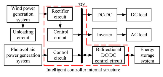
Figure 1.
Overall architecture of the power supply system.
• Power generation part:
It consists of a 1200 W/48 V wind turbine and 750 W/30 V PV array (three parallel boards with a 250 W single board). The three-phase electricity generated by wind power is converted into DC power through a three-phase rectifier bridge. The rectified wind power and photovoltaic arrays output direct current are respectively boosted by respective control circuits, and then connected to the intermediate DC bus; the energy flows in one direction. The boost circuit is composed of the boost converter, which is efficient and easy to achieve maximum power tracking [9].
• Energy storage part:
The battery pack plays the role of energy regulation and balance load in the power supply system [10]. The capacity of this system is 1421 Ah/24 V, so there are 14 batteries (two in series and seven in parallel) with a 200 Ah/12 V single battery. Electrical energy flows between the DC bus and the energy storage system through a bidirectional DC/DC. The bidirectional DC/DC adopts a Buck/Boost structure, which is a Buck charging mode from the bus side to the storage side, and a Boost discharge mode from the storage side to the bus side. The circuit can realize the charging and discharging of the battery, and can achieve overcharging and over discharge protection at the same time.
• Power consumption part
The power consumption part is 757 W for AC load and DC load, and the DC load power is very small, which is directly provided by the energy storage battery. The AC load power is supplied through the inverter, which converts the DC power in the left busbar into AC power for the load. At the same time, the inverter can stabilize the bus voltage, and also help to improve the quality of the load supply [11].
• Intelligent control part
The intelligent control part includes wind power rectifier circuit, unloading circuit and its Boost control circuit, photovoltaic power generation Boost control circuit and bidirectional Buck/Boost circuit. The specific parameters of each circuit component need to refer to the maximum load power consumption and average daily power generation. At the same time, the maximum power consumption is helpful to select the appropriate inverters, and the average daily power generation is helpful to allocate the capacity of wind, light and storage reasonably [12].
3. Controller Hardware Design
The controller adopts STC8A8K64S4A12 as the control core. The hardware circuit includes the control core and its peripheral circuits, signal acquisition and conditioning circuit, isolated drive circuit, auxiliary power supply circuit, wind power generation circuit, photovoltaic power generation circuit, battery charge and discharge circuit and load control circuit.
3.1. Control Core and Its Peripheral Circuits
The main circuit consisted of the main control unit circuit using STC8A8K64S4A12 as a control center, a 2.5 V reference source circuit, a system operation indication circuit, a USB serial communication and an ISP download circuit.
3.1.1. Main Control Unit
The STC8A8K64S4A12 MCU is the latest generation of the enhanced 8-bit MCU introduced by Hongjing Technology in 2017. It does not require an external crystal and reset circuit. There are 25 I/O ports used in this design. The function selection is shown in Table 1.

Table 1.
Functional Selection of I/O Port.
3.1.2. 2.5 V Reference Source Circuit and System Operation Indication Circuit
Usually, the AD converter inside the main control chip uses the internal power supply as a reference to calculate the sampling value of the AD channel. When the internal power supply has fluctuations, although the main control can work stably, the AD sampling will be inaccurate, so an additional stable voltage is added as a reference for AD acquisition and conversion. The 2.5 V reference source consisting of TL431 is used here, and its circuit is shown in Figure 2. Figure 3 shows the controller operation indication, the red light indicates the system failure, and the green light indicates that the system is operating normally.
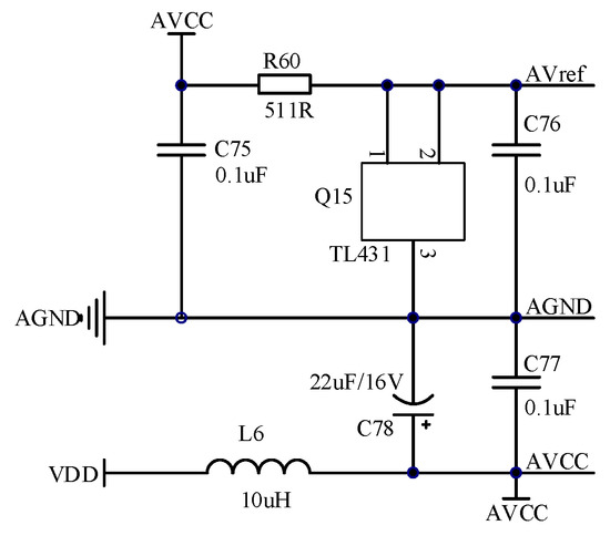
Figure 2.
2.5 V reference source circuit.
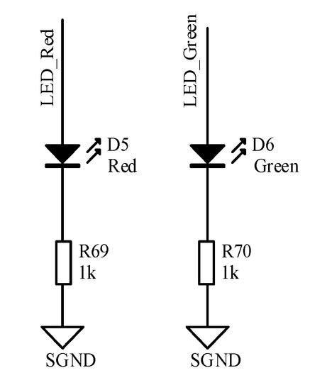
Figure 3.
System operation indication circuit.
3.1.3. USB Serial Communication and ISP Download Circuit
The upper side of Figure 4 is the USB serial communication circuit, which is used to display some data of the program running through the serial port assistant, which is helpful for debugging the program. It uses the CH340 chip for level conversion, which realizes communication between the MCU and the computer. Compared with the traditional 9-pin serial interface, it greatly reduces the component size and is more convenient. The lower side buttons, triodes and Light Emitting Diode (LED) lights enable program download and power indication.
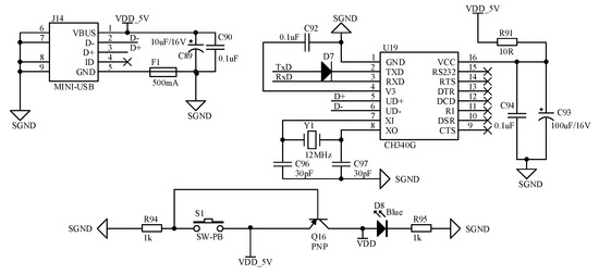
Figure 4.
Serial communication and ISP circuit.
3.2. Signal Acquisition and Conditioning Circuit
3.2.1. Voltage Acquisition and Conditioning
The voltage acquisition and conditioning circuit is show in Figure 5.
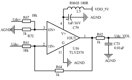
Figure 5.
Voltage acquisition and conditioning circuit.
In the voltage acquisition, a differential proportional amplifier circuit is used, which is composed of a single-supply rail-to-rail input and output four-channel operational amplifier TLV2374 produced by Texas Instruments and its peripheral resistors. It has a high common-mode signal rejection ratio and high input resistance. When the pin of the control core is used for ADC acquisition, the maximum input is 5 V, and the maximum DC voltage in the entire power supply system does not exceed 90 V, so the voltage division ratio is 18:1. The voltage acquisition output is input to the ADC acquisition pin of the main control chip through the RC low-pass filter circuit.
3.2.2. Current acquisition and conditioning
In this paper, the current detection chip ACS712-30A based on the Hall induction principle is used. The load current of one channel is shown in Figure 6a.
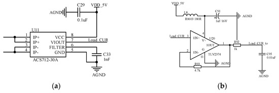
Figure 6.
Current collecting and conditioning circuit: (a) Load current acquisition circuit; (b) Signal conditioning circuit.
The chip-level Hall current sensor is connected in series in the current loop, its peripheral circuit is simple; it has a milli-ohm path resistance built in; the primary current flows only from the inside of the chip, and there is no contact with the secondary circuit, so that the primary secondary side is isolated. The operating temperature is −40 °C to 85 °C, the accuracy of the full temperature range is ± 1.5%, The input-domain output in the range of measurement has a good linear relationship Vout = 0.5Vcc + Ip*0.066. The Vcc power supply of the ACS712 is generally recommended to use 5 V, and the output voltage signal is between 0.5 V and 4.5 V. Figure 6b shows the signal conditioning section. The four-channel TLV2374 forms a voltage follower to increase the output impedance, and then filters out the interference through the low-pass filter circuit and outputs it to the ADC pin of the master.
3.3. Isolated Drive Circuit
3.3.1. Optocoupler Isolation
This paper selects the ON Semiconductor HCPL2631 optocoupler to realize the power circuit cut-out and transmission of the Unicom signal and the high-speed transmission of the switching tube PWM signal. The HCPL2631 features a dual-channel high-speed optocoupler with 10Mbps data rate and 10 kV/μs common-mode rejection (CMR) to minimize control signal delay and distortion. One of the isolation circuits is shown in Figure 7.
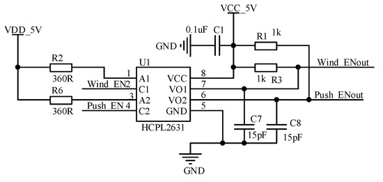
Figure 7.
Isolation circuit.
3.3.2. MOSFET Driver
The drive circuit of the power MOS transistor selects UCC27211 and UCC27324 of Texas Instruments, as shown in Figure 8.
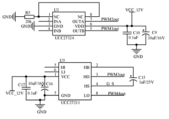
Figure 8.
MOSFET drive circuit.
The UCC27211 is a high/low side gate driver with a peak current of 4 A. Its input and output are complementary symmetrical PWM signals with dead zones for driving bidirectional Buck/Boost circuits. The low-side and high-side gate drivers are independently controlled, and achieve a 2 ns match between the turn-on and turn-off of each other, while providing an undervoltage lockout. If the drive voltage is below the rated threshold voltage, a symmetric on/off mode of operation is provided, and the output is forced low. A bootstrap diode rated at 120 V is also integrated on the chip, eliminating the need for an external discrete diode. These features greatly facilitate the use of the driver chip, and simplify the circuit design. The UCC27324 is a low-side driver with dual 4 A peak current capability. The input and output are two independent PWMs, which are used to drive Boost circuit switches for wind power and photovoltaic power generation, respectively.
3.4. Auxiliary Power Circuit
There are five power supply targets for the auxiliary power supply, namely the STC8A8K64S4A12 control chip, op amp, optocoupler, current sensor and MOS transistor driver chip. The power supply of the STC8A8K64S4A12, op amp, optocoupler and current sensor is 5 V, and the power supply of the MOS transistor driver chip is 12 V. Then the power circuit design is shown in Figure 9.
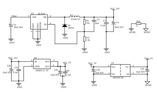
Figure 9.
Auxiliary power circuit.
The electric energy is provided by a storage battery, after passing through the XL7035, it becomes a DC voltage supply of 12 V for the MOS transistor driver chip. XL7035 is an efficient, high voltage step-down DC-DC converter. It provides a wide input voltage range from 10 V to 80 V. The output voltage is adjustable from 1.25 V to 20 V, providing a maximum 1 A output current capability. The 5 V power supply is then supplied to the main control chip, op amp and current sensor through the B0505S isolated DC/DC. The combination of the optocoupler and the B0505S achieves a double isolation of the signal and of the power supply, respectively, separating the power ground from the analog ground and the digital ground. The 0 Ω resistor connection between the analog ground and the digital ground isolates the interference, ensuring the stability of the circuit.
3.5. Wind Power Generation Circuit
Wind power circuit is a Boost structure, as shown in Figure 10.
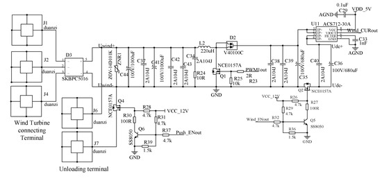
Figure 10.
Wind power generation circuit.
First, three-phase AC becomes DC with a rectifier bridge, then the obtained DC passes through a varistor and an input capacitor. After being boosted and filtered, the direct current flows into the DC bus through a current sensor. The function of the varistor is to clamp the voltage and absorb excess current to protect the sensitive device when the circuit withstands overvoltage.
The switch tube Q4 is used to open the unloading path, and the Q2 is used to open the output of the ventilation power generation circuit.
The rated power of the wind turbine is 1200 W, the rated input voltage is 48 V, the DC bus voltage is 72 V, the inductor ripple factor is 10%, the voltage ripple factor is 1%, and the switching frequency of the main power tube is set to 48 kHz. After calculation, the main circuit inductance of this wind power generation is 220 μH (microhenrys), the output filter capacitor is 680 μF (microfarads), and 0.1 μF, and the input capacitance is 1000 μF and 0.1 μF. The N-channel MOS transistor of NCE0157A type is selected as the power transistor. The VDS voltage of the transistor is 100 V, the ID is 57 A, and the on-resistance RDS is less than 17 m. It has excellent performance and low power consumption. The continuous current diode V40100C is a MOS Schottky diode with ultra-low conduction voltage drop of 0.38 V. The forward current is 40 A, the voltage is 100 V, and the reverse voltage is 150 V.
3.6. Photovoltaic Power Generation Circuit
The main circuit of photovoltaic power generation is shown in Figure 11. This circuit is also a Boost structure, and will not be described here. The rated power of the PV array is 750 W, the rated input voltage is 30 V, the inductor ripple factor is 10%, the voltage ripple factor is 1%, and the switching frequency of the main power tube is set to 48 kHz. After calculation, the main circuit inductance of the photovoltaic power generation is taken as 220 μH, the output filter capacitor is 680 μF and 0.1 μF, and the input capacitance is 1000 μF and 0.1 μF.
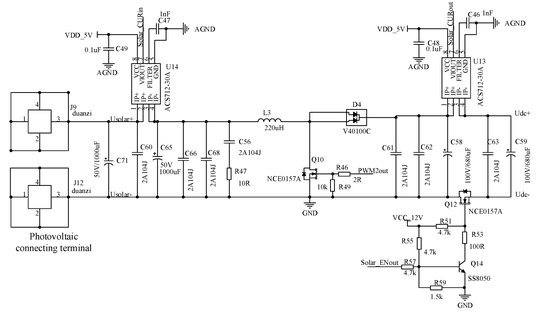
Figure 11.
Photovoltaic Power Generation Circuit.
3.7. Battery Charge and Discharge Circuit
The charge and discharge circuit of the battery is a Buck/Boost structure, as shown in Figure 12. When the circuit is in Buck mode, the circuit depends on the duty cycle of the upper tube, and the lower tube is equivalent to a freewheeling diode. When the circuit is in Boost mode, the circuit depends on the duty cycle of the down tube, and the upper tube is equivalent to the isolation diode. The DC bus voltage is 72 V, the maximum input current is 28 A, the output voltage is 24 V, and the maximum charging current is controlled within 30 A. The inductance value is 150 μH. The bus-side filter capacitor is 680 μF and 0.1 μF, and the battery-side filter capacitor is 1000 μF and 0.1 μF.

Figure 12.
Battery charge and discharge circuit.
3.8. Load Control Circuit
The load control circuit is shown in Figure 13. The bus current is connected to the terminal through the load current sensor, and Q3 controls the on and off of the side.
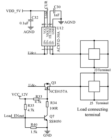
Figure 13.
Load control circuit.
4. Controller Software Design
In this section, based on the Keil programming environment, the software part of the power supply system for aerosol stereo cultivation is compiled in C language. The system software is mainly divided into three parts: The system initialization program, main program and interruption service program. The overall structure of the software is shown in Figure 14. The acquisition control of the ADC, wind turbine, photovoltaic control, battery charge and discharge control and unloading control are sequentially executed every 5 ms in the main timer interrupt service routine. In the serial interrupt service program, it mainly completes the communication between the serial port and PC, and sends the related data and status information written in the main program to the serial assistant.
Figure 14.
Overall Software Architecture.
When the system is powered on and reset, a series of initialization work must be completed first. First, all variables defined in the system should be initialized, and then the input and output mode of the GPIO port should be configured. After the port configuration is completed, the LED should be started to indicate the current working state of the system immediately. Output I/O initialization refers to an initial value for the switches and PWM switches that control whether the main circuit is connected or not. Generally, the output is disconnected at 0. The initialization work of the serial port is to define the working mode, baud rate, sending permission, interrupt permission, interrupt priority, and so on. The initialization of the ADC is to set the number of ADC channels, sampling speed, result storage form and ADC power. The main task of timer initialization is to set the mode of the timer, initial value, interrupt enable, and so on. PWM initialization is mainly to set the period of the PWM counter and the initial value of the primary and secondary flips of each PWM channel. Interrupt initialization is mainly to open the CPU total interrupt, timer interrupt and serial interrupt and to set high priority. After these initializations are completed, the program begins to run in the main program loop. After the initialization, the system starts to enter the infinite loop of the main loop to perform input and output control, protection control and state switching control. The flow chart is shown in Figure 15.
Figure 15.
Main program flow chart.
The running of the main program mainly depends on the status flag bit. The acquisition of voltage and current information is completed in the interruption of the timer. After the relevant data acquisition is completed, there will be a set flag set to 1 (Finishflag = 1). After the detection of the mark bit in the main program, the voltage, current and system working state will be written into the serial transmission buffer in the form of a string, and sent to the serial port assistant of the PC. After the transmission is completed, the set flag is set to zero (Finishflag = 0). If the bit is not set to 1, the system’s working status is judged directly.
The judging link of the system working state is mainly to judge whether there is over-voltage, over-current, short circuit, no-load, and so on. If it does not happen, the current indicator state and the corresponding pin control state will be maintained, and the next step will be taken. If one of them occurs, the protection mechanism is activated, the fault is judged and the relevant flag bit is set to 1 (Error = 1), thus turning on the status indicator. If the fault flag of the corresponding circuit is detected as Error = 1 in the main timer, the output and load of the circuit are directly disconnected. At the same time, the fault information is sent to the serial port to start the slave timer. The slave timer closes after 5 ms, reopens the output and judges the working state of the system. If normal, set Error = 0, return to the normal indicator state, maintain the output state of the circuit, and close the load.
The next step in the energy analysis is based upon the power management strategy of the power supply system in Table 2. Based on the collected information, the relevant logical judgments are made to make decisions. The relevant flag bit is judged in the timer interrupt, and the control program is started.
Table 2.
Electric Energy Management Strategy of the Power Supply System.
The control strategies adopted in the polar night and non-polar night aerosol three-dimensional cultivation power supply systems are different. In the polar night, the temperature is very low, where the average temperature is close to −15 °C, and the excess power of the wind power is utilized for heating rotating parts to ensure the stability of the operation of the fan. The non-polar night period includes the polar day period, and the photovoltaic power generation part of the power supply system is very stable, which maximizes the use of this part to supply power to the load. When the photovoltaic power is greater than the load power, if the acceptable charging power of the battery is less than the residual power supply, the photovoltaic system needs to be operated at constant voltage, that is, the output voltage is regulated by closed-loop control to maintain the constant DC bus voltage.
5. Experiment
After completing the software and hardware debugging of the module, a 100 W power generation system, composed of a 50 W vertical axis wind turbine and 50 W photovoltaic panels, was tested in the laboratory environment. The test platform is shown in Figure 16.
Figure 16.
The test platform.
• Wind power system
The blades of the 50 W vertical axis wind turbine are dismantled, and the flange coupling is used to connect with the small AC speed-regulating motor. The AC speed-regulating motor drives its rotation and indirectly realizes the power output of the vertical axis wind turbine at different wind speeds, by adjusting the speed of the AC motor. The right side of the AC variable speed motor is a speed governing device, and the vertical axis wind turbine is a ruggedized structure. See the lower side of Figure 16.
• Photovoltaic systems.
The black part on the upper side of the picture is a 50 W photovoltaic module, which is made of reinforced tempered glass and an aluminum alloy frame. During the power generation experiment, it will be placed under outdoor sunlight.
• Energy storage.
On the left side of the picture is a lead-acid battery with a capacity of 200 AH, which can work reliably from −40 °C to + 75 °C.
• Load.
On the right side of the picture is a high-power load resistor for consuming wind power, photovoltaic power and battery power.
• Controller.
In the middle position at the center is the wind-solar complementary controller. After making the circuit designed above into PCB board, it is welded by low temperature resistant components.
Next, the waveforms of wind power generation, photovoltaic power generation and charge-discharge circuit are tested respectively. The test waveform of the wind power circuit is shown in Figure 17.
Figure 17.
Wind power circuit test waveform.
The green line is its output voltage, which is 20 V per cell and about 72 V. The yellow line is the GS waveform of the power switch MOS transistor. The value of each cell is 5 V, its frequency is 48 kHZ, the amplitude is 12 V, and the duty ratio is 60% at rated output. The blue line is the DS waveform of the power switch MOS transistor, each cell is 50 V, and its peak value is the same as the output voltage. It can be seen from the figure that the output voltage is basically stable, but the voltage spikes appear in the GS, DS, and output voltage waveforms at the instant when the power switch is turned on, mainly because the circuit does not have a design peak absorption.
The test waveform of the photovoltaic power generation circuit is shown in Figure 18.
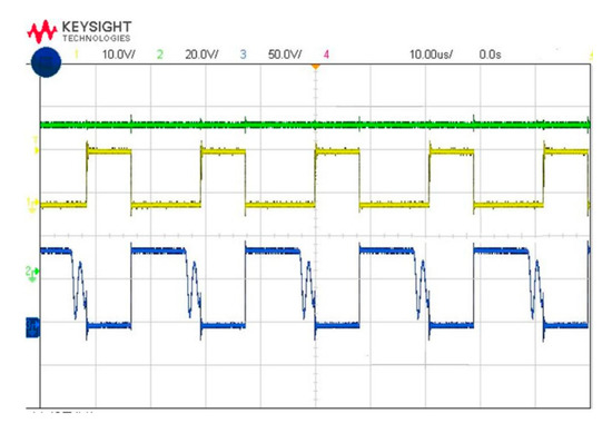
Figure 18.
Photovoltaic circuit test waveform.
The green line represents the output voltage of the photovoltaic circuit, and the yellow and blue lines are the GS and DS waveforms of the power switch MOS tube, respectively, and the unit cells of each waveform represent 10 V, 20 V, and 50 V, respectively. It can be seen from the figure that the output voltage of the photovoltaic power generation circuit is about 72 V, the duty ratio of the power switch tube is 38.83%, the amplitude of the switching tube GS is 12 V, but the peak-to-peak value reaches 17.3 V, which is much smaller than that of switch tube of wind power generation circuit. The amplitude of the DS waveform is the same as the output voltage, and the waveform oscillation occurs between the switching off and the switching on, mainly because the inductance part works in the intermittent mode at this time.
The MOS tube drive waveform of the charge and discharge circuit during charging is as shown in Figure 19.
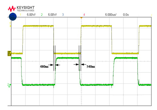
Figure 19.
Power MOS tube driving waveform when the charging and discharging circuit is charged.
The yellow line in the figure is the GS waveform of the main power switch MOS with a duty cycle of 53.155%, and the green line is the GS waveform of the vice-transistor with a duty cycle of 41.718%. The two waveforms complement each other, and the turn on and turn off dead zones are 540 ns and 480 ns, respectively. The value of each cell in the figure is 5 V, and the amplitudes of the two waveforms are 12 V. However, voltage spikes occur at the turn-on and turn-off time, with peak values reaching 13.1 V and 13.9 V respectively.
6. Conclusions
This paper designs the hardware and software of the controllable micro-environment aeroponic, stereoscopic cultivation wind and solar hybrid power supply system. This paper also designs the hardware and software of the controllable micro-environment three-dimensional cultivation wind and solar hybrid power supply system.
The design of STC8A8K64S4A12 control core and its peripheral circuits, signal acquisition and conditioning circuit, isolated drive circuit, auxiliary power supply circuit and power circuit are completed. The schematic and PCB drawing were completed in the Altium Designer environment, and the controller hardware was fabricated using the purchased components. The system control program was written using Keil. Finally, the power supply system controller hardware was debugged and tested.
Author Contributions
Conceptualization and writing-original draft: Y.C.; investigation: C.M.; methodology and validation: X.H.; writing—review and editing: Y.D.; software: R.C.
Funding
This research was funded by the Natural Science Foundation of Shanxi Province, grant number 201701D121127, and by the Key Research and Development Program of Shanxi Province, grant number 201803D221028-2.
Acknowledgments
Xiaomin Chang provided valuable advice on the study idea and write-up. Thanks also go to Zaihe Shen, Wentao Wu, Yuefeng Jiang, Yanzhao Hao, Min Cao and Jinmeng Wu for their assistance during the research.
Conflicts of Interest
The authors declare no conflict of interest.
References
- Arenella, V.; Gabriele, P.; Leccese, F.; Cagnetti, M.; Maiolo, L.; Pecora, A.; De Francesco, E.; Đurović-Pejčev, R. Procedure for the space certification of a controller for soilless cultivation. In Proceedings of the 2016 IEEE Metrology for Aerospace (MetroAeroSpace), Florence, Italy, 22–23 June 2016; pp. 359–364. [Google Scholar] [CrossRef]
- Ma, X.W.; Wu, W.H.; Sun, W. Discussion on Food Security of Antarctic Scientific Research in Winter. Geomatics Spatial Inf. Technol. 2006, 6, 9–11. [Google Scholar] [CrossRef]
- Hou, X.N. Controllable micro-environmental aeroponic stereoscopic cultivation power supply system design and power management. Master’s Thesis, Taiyuan University of Technology, Taiyuan, China, 2019. [Google Scholar]
- Sun, Z.P.; Liu, T.; Lin, S.S. Effect of Aeroponics on the Growth, Yield and Quality of Tomato Plant. J. Shenyang Agric. Univ. 2006, 37, 488–490. [Google Scholar] [CrossRef]
- Zhang, J.G.; He, C.M.; Ling, M.; Wang, H.F. Review on the Application and Research Progress of Aeroponic Cultivation. For. Environ. Sci. 2017, 33, 130–134. [Google Scholar] [CrossRef]
- Shen, Z.H. Design and Implementation of Controllable Micro-environment Aerosol Stereo Cultivation Monitoring System. Master’s Thesis, Taiyuan University of Technology, Taiyuan, China, 2019. [Google Scholar]
- Pasquali, V.; D’Alessandro, G.; Gualtieri, R.; Leccese, F. A new data logger based on Raspberry-Pi for Arctic Notostraca locomotion investigations. Measurement 2017, 110, 249–256. [Google Scholar] [CrossRef]
- Hou, X.N.; Chen, Y.; Ma, C.Y. Antarctic aerosol Stereo cultivation room wind and solar hybrid power supply system. Sci. Technol. Eng. 2018, 18, 140–146. [Google Scholar]
- Guan, X.L.; Xu, Y. The parameter design of 5kW solar energy MPPT circuit. World Power Supply 2011, 8, 50–53. [Google Scholar]
- Xi, X.Q.; Dou, Y.K.; Dou, R.F.; Ma, R.J.; Hu, S.Y. Investigation and simulation of wind-solar complementary system control strategy in Zhongshan Station of Antarctic. Sci. Technol. Eng. 2017, 17, 72–79. [Google Scholar] [CrossRef]
- Chen, L. The Implementation of the Photovoltaic Grid-Connected Power Generation System. Master’s Thesis, North China Electric Power University (BAODING), Beijing, China, 2009. [Google Scholar]
- Chen, H.J. Wind and Solar Hybrid Power Generation Application Technology, 1st ed.; Chemical Industry Press: Beijing, China, 2016; pp. 145–166. [Google Scholar]
© 2019 by the authors. Licensee MDPI, Basel, Switzerland. This article is an open access article distributed under the terms and conditions of the Creative Commons Attribution (CC BY) license (http://creativecommons.org/licenses/by/4.0/).