1. Introduction
This paper presents the hardware implementation and characterization of a novel Delta-Differential One-Way Ranging (
DOR) technique based on spread-spectrum waveforms [
1,
2]. The relative angular position of a spacecraft with respect to known radio sources (typically, quasars) is currently determined by means of differential phase measurements using Very Long Baseline Interferometry (VLBI) technique [
3,
4] according to CCSDS 500.1-G-1
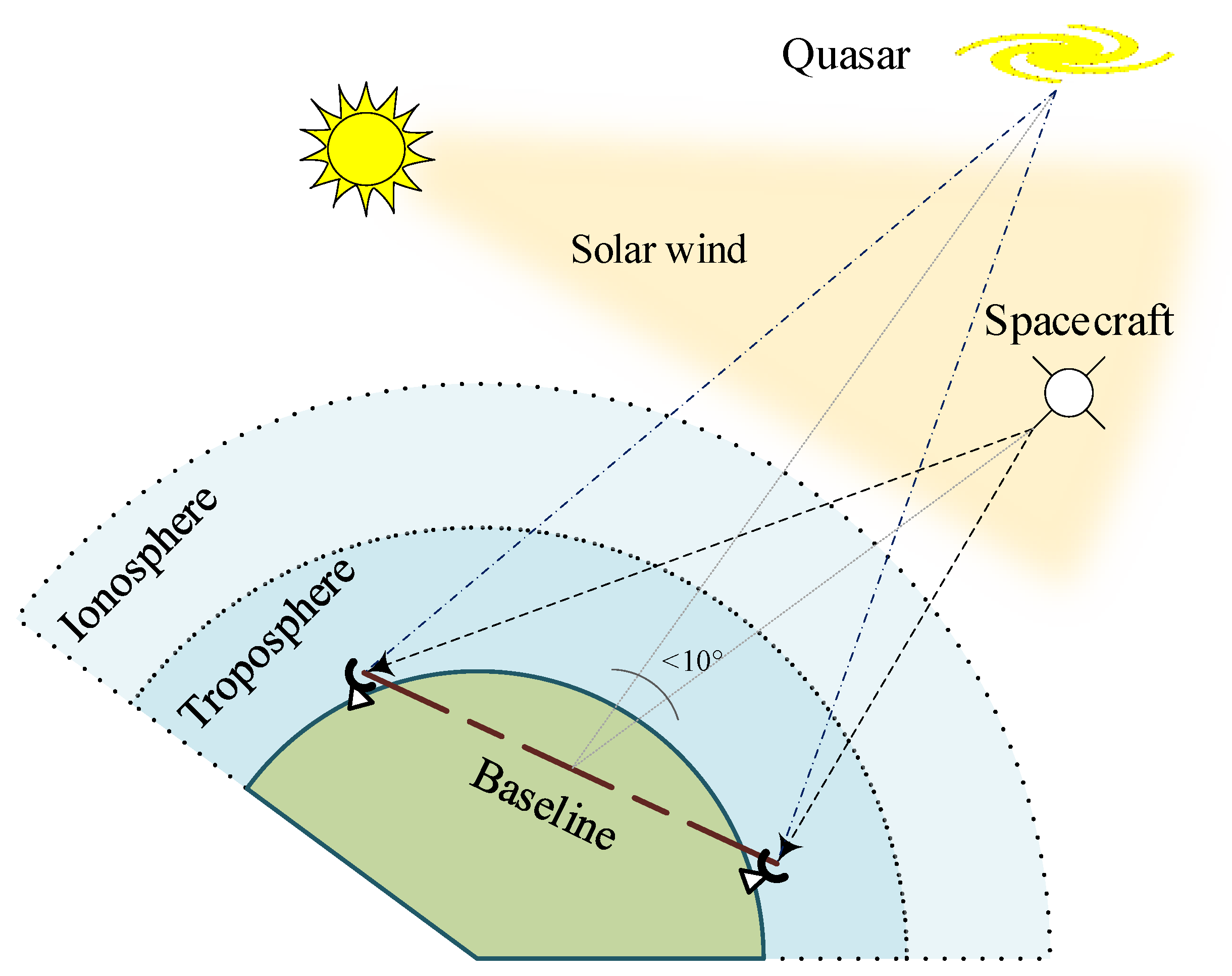
Delta-DOR Technical Characteristics and Performance. In practice, the difference in arrival times of spacecraft radio signals at two widely separated ground stations is accurately measured, along with similar differential phase measurements of a nearby quasar. The quasar, being one of the radio sources defining the International Celestial Reference Frame (ICRF), has known angular coordinates and can serve as a fiducial landmark to reference the spacecraft phase (
Figure 1).
The spacecraft location is measured with excellent accuracy relative to the ICRF frame [
5]. The ESA
DOR system attains consistently angular accuracies of a few nanoradians (corresponding to delays in the order of
s). Precise angular measurements are extremely valuable for both spacecraft navigation and scientific investigations of Solar System dynamics. The knowledge of the angular position proves very important, especially in the planetary approach phase in order to prepare and execute the planetary orbit insertion.
Although Doppler observables also provide angular information,
DOR observations are intrinsically more accurate and less dependent on the dynamical model of the spacecraft [
6,
7]. The targeting of the capture maneuver (for an orbiter) or the Entry, Descent, and Landing (EDL) phase greatly benefit from, and even rely on, previous
DOR observations. Accurate Solar System bodies and satellite ephemerides are crucial for Solar System exploration. In addition, the generation of precise ephemerides requires an accurate formulation of Solar System dynamics in the context of a fully relativistic model. Conversely, tracking the motion of Solar System bodies is an excellent experimental tool to test the adopted laws of gravity. The Solar System constitutes indeed the cleanest environment to carry out determinations of the space-time metric in the weak field limit, and to assess the range of validity of general relativity. The observable of choice for Solar System dynamics investigations are range and
DOR. The two set of measurements complement each other, with
DOR providing unique information in the out-of-plane components of planets and satellites positions. The orbits are determined by first referencing the orbit of the spacecraft to the planetary body using Doppler measurements, and then linking the body’s position to a Solar System barycentric frame by means of angular and range measurements. Other interesting applications of interferometric techniques are related to the relative positioning of two spacecraft, landers, or a lander and an orbiter. This technique, called Same Beam Interferometry (SBI) [
8], was originally proposed in a configuration with two antennas tracking simultaneously two probes in one-way mode.
However, SBI can be considered in a simpler configuration where a single ground antenna tracks, simultaneously in two-way mode, two probes separated by a small line-of-sight angle (0.5 degrees or less). This powerful method allows a considerable improvement in the positioning of a probe when the orbit (or the position) of the second one is well determined. The coherent downlink signals coming from each probe are combined to form the differential phase, proportional to the relative distance between each probe of the pair. In the case of two (or more) landers, SBI would provide very accurate measurements of tides and rotational state of a planetary body, which are used in geophysical models to constrain the interior structure and evolution.
The scenario where two landers are deployed on the surface of Mars is particularly interesting since differential range accuracies of the order of 1–10 mm can be attained. SBI measurements to a network of landers on the moon would provide differential range at least an order of magnitude more precise, thus providing useful geophysical information on the lunar interior.
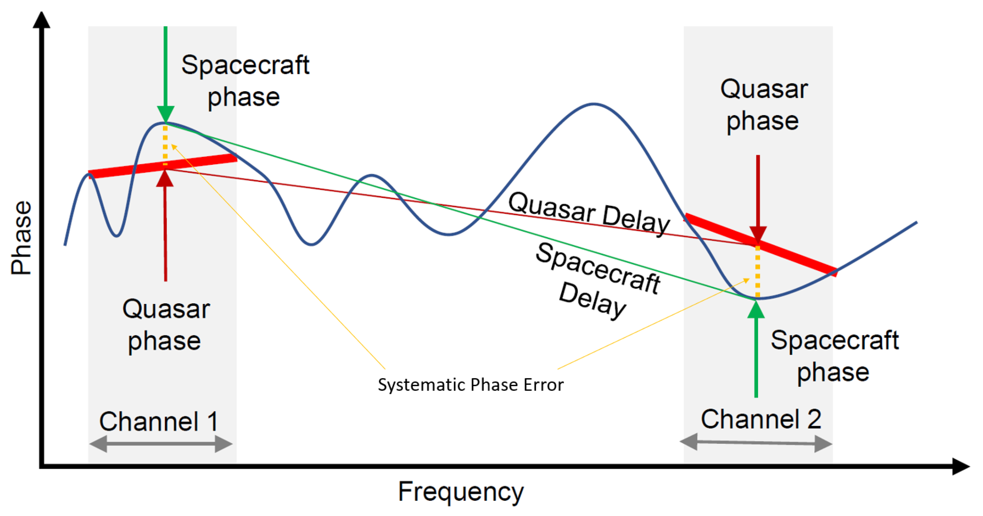
This level of accuracy can be obtained by means of two-way radio links in X or Ka band enabled by suitably designed digital transponders and spread spectrum radio links, as described in this paper. Spread spectrum signals not only allow a reduction of the differential group delays in
DOR and SBI measurements, but also enable simultaneous communications to multiple spacecraft from a single antenna, a scenario that is already occurring at Mars. The spacecraft group-delay measures involve differencing the measured phase of two or more discrete tones transmitted by the spacecraft. The measured phase difference between a pair of tones, divided by their frequency separation, is the primary group-delay observable. This is in contrast to the several-MHz bandpass used to measure the quasar group delays, therefore a systematic error is induced in the
DOR measure, as outlined in
Figure 2.
The blue curve shows the phase dispersion as a function of frequency, while the green line shows the average linear behavior. At the spacecraft tone frequency (arrows), the measured phase differs between the narrowband spacecraft measurement (green) and the wideband quasar measurement (red), resulting in systematic phase error. To minimize the systematic error, the on-board synthesized
DOR signal should resemble the quasar one as much as possible [
9]. Thanks to the differential nature of the measurement, the difference between the spacecraft and quasar delays produces an observable that minimizes calibration errors due to instrument dispersion, especially the ones due to phase ripples in the acquisition filter, thus providing enhanced performances [
10]. The recent advancements in the field of on-board microelectronics, e.g., Digital Signal Processing cores for space applications, are enabling factors to develop the newest
DOR paradigm based on broadband observables: Wideband
DOR.
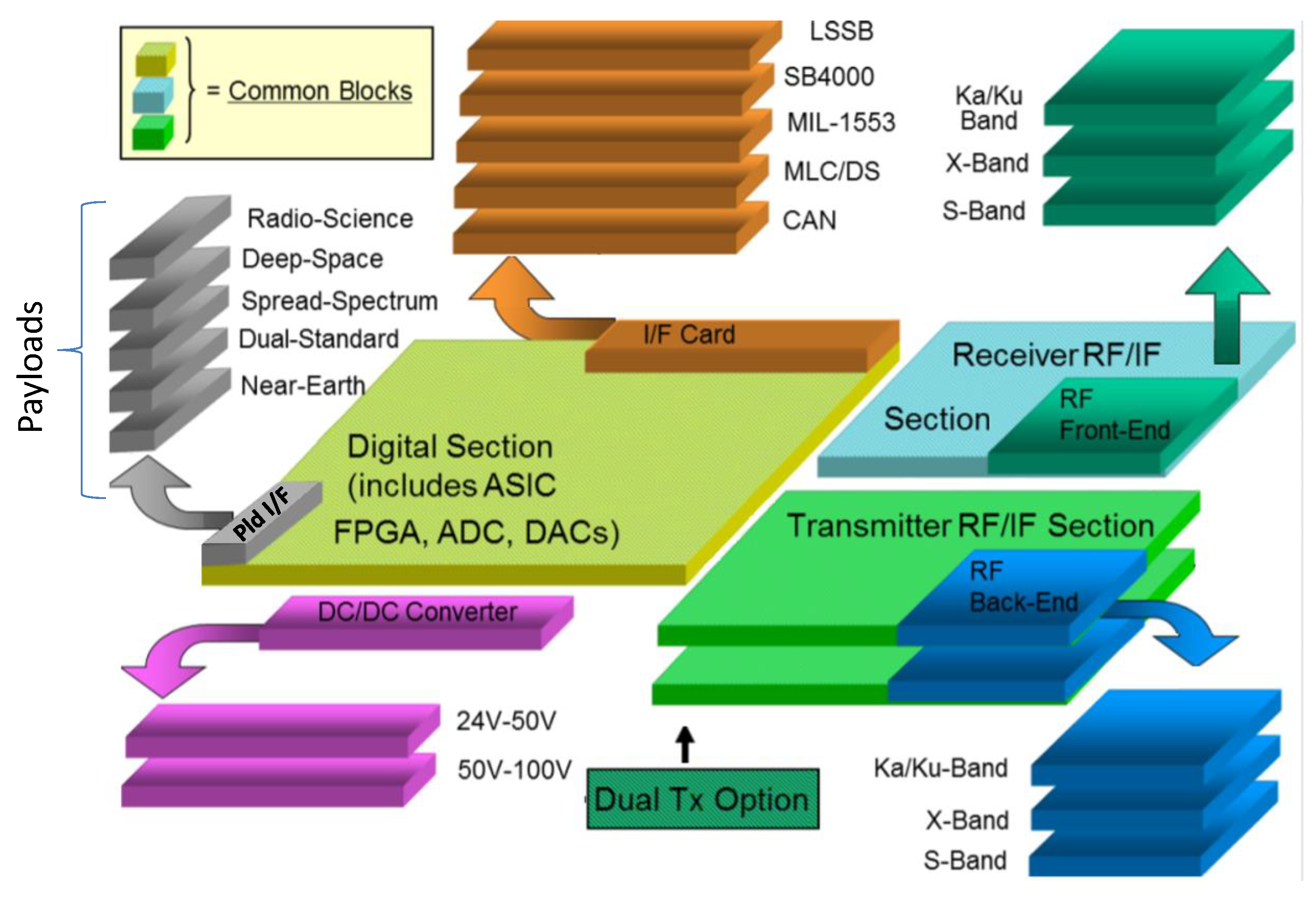
2. Thales Alenia Space Transponder Platform
The core of the novel Wideband
DOR (W-
DOR) will be integrated in the new Thales Alenia Space (TAS) Transponder Platform based on the TAS deep-space transponder architecture and depicted in
Figure 3.
This transponder has been conceived as a common platform, composed of common blocks coupled with custom parts. The common platform includes: the Digital Section (ASIC, FPGA, DACs, ADC), the Transmitter Radio Frequency (RF)/Intermediate Frequency (IF) section and the Receiver RF/IF section. The custom parts include: the DC/DC Converters, the Programmable Read-Only Memory (PROM) Interface, the RF Front-End and Back-End sections and the Interface Card. The platform approach allows the TAS transponder to be very flexible and reconfigurable in terms of physical modules and mapped cores on the internal FPGA. Different missions will require different sets of DC/DC Converters, programmable read-only memories, interfaces and RF front-end and back-end. Conversely, the transponder core, composed of the digital and RF/IF sections, will remain unchanged [
11,
12]. The new transponder named Flexible Autonomous Transponder (FAT) has been derived from the TAS transponder heritage regarding Deep-Space, Radio-Science, Near Earth and Secure Spread-Spectrum TT&C product lines. The different functions are implemented in the following modules:
Dual Band Receiver Analogue Module
Digital Module
X-Band Transmitter Analogue Module
Ka-Band Transmitter Module
Baseplate Module
The FAT architecture has been conceived to support, by means of the same hardware, different mission scenarios and applications. For example, deep-space missions such as BepiColombo and JUICE feature regenerative ranging with low chip rate (3 Mcps) and radio science experiments with high chip rate regenerative ranging (24 Mcps) for accurate ranging measurements. The FAT digital core is conceived around the Ka-band Transponder (KaT) ASIC that fully supports all required modulation schemes and processing needs. The KaT ASIC has been developed in the frame of BepiColombo/MORE program, in which a new digital platform has been developed by TAS aiming to cover all TT&C modulation standards (spread-spectrum, FM, and PM) and mission profiles, from deep-space to near-Earth.
Moreover, it includes a powerful microprocessor, i.e., the LEON2-FT [
13], implementing the first System-on-Chip (SoC) devoted to on-board TT&C missions. Through the AMBA bus, the LEON2-FT is able to configure and control the different DSP functional blocks such as: carrier processing (that receives samples from the ADC), telecommand processing, ranging channels, telemetry block (that receives telemetry data from the on-board computer for down-link modulation), DDS parameters and functions for the Rx and Tx blocks. Moreover, through the memory bus, the KaT embedded microprocessor can access external devices for configuration and control. In particular, the LEON2-FT can access the FPGA where the novel W-
DOR core is loaded.
3. W-ΔDOR Hardware Implementation
This section provides a description of the W-
DOR DSP core hardware implementation. The down-link (DL) signal is Equation (
1).
It is the modulation of a X/Ka-band carrier by means of pseudo-noise phase components. In Equation (
1),
A represents the signal amplitude,
is the X- or Ka-band carrier frequency,
represents telemetry and command signals and
is the spread spectrum component of the W-
DOR signal. This method is proposed in [
1] with the purpose of compatibility with the BepiColombo X/Ka Deep-Space Transponder design [
11]. The signal represented in W-
DOR part is the summation of
N sub-carriers of frequency
.
They are modulated by pseudo-random noise sequences of amplitude .
3.1. W-ΔDOR DSP Core Architecture Description
The W-ΔDOR DSP core is implemented in the FPGA available in the transponder digital section and generates the signal defined by Equation (
2). Detailed system specifications are provided in [
1]. The system clock frequency is
MHz where
is
MHz for compatibility with the work in [
1,
11]. The main technical specifications are:
Selectable chip rates: , , and for tuning the spectrum width of the DOR observables;
Selectable sub-carrier tones: and , for the spectrum allocation of the observables;
Complete in-flight parameters reprogrammability; and
Backward compatibility with narrowband DOR.
The LEON2-FT microprocessor is in charge to enable/disable the core. Moreover, the LEON2-FT can read and write the W-
DOR core parameters by using a register file internal to the FPGA. These registers contain different parameters such as chip rates and sub-carriers frequency words. A control register is also included to enable and reset the W-
DOR core and to set up the narrowband compatibility mode. The on-chip communication occurs through a dedicated bus controlled by a custom IP core called LEON2-FT Interface Bus Controller. The W-
DOR core has two outputs: Root Raised-Cosine (
RRC) and Non-Return-to-Zero (
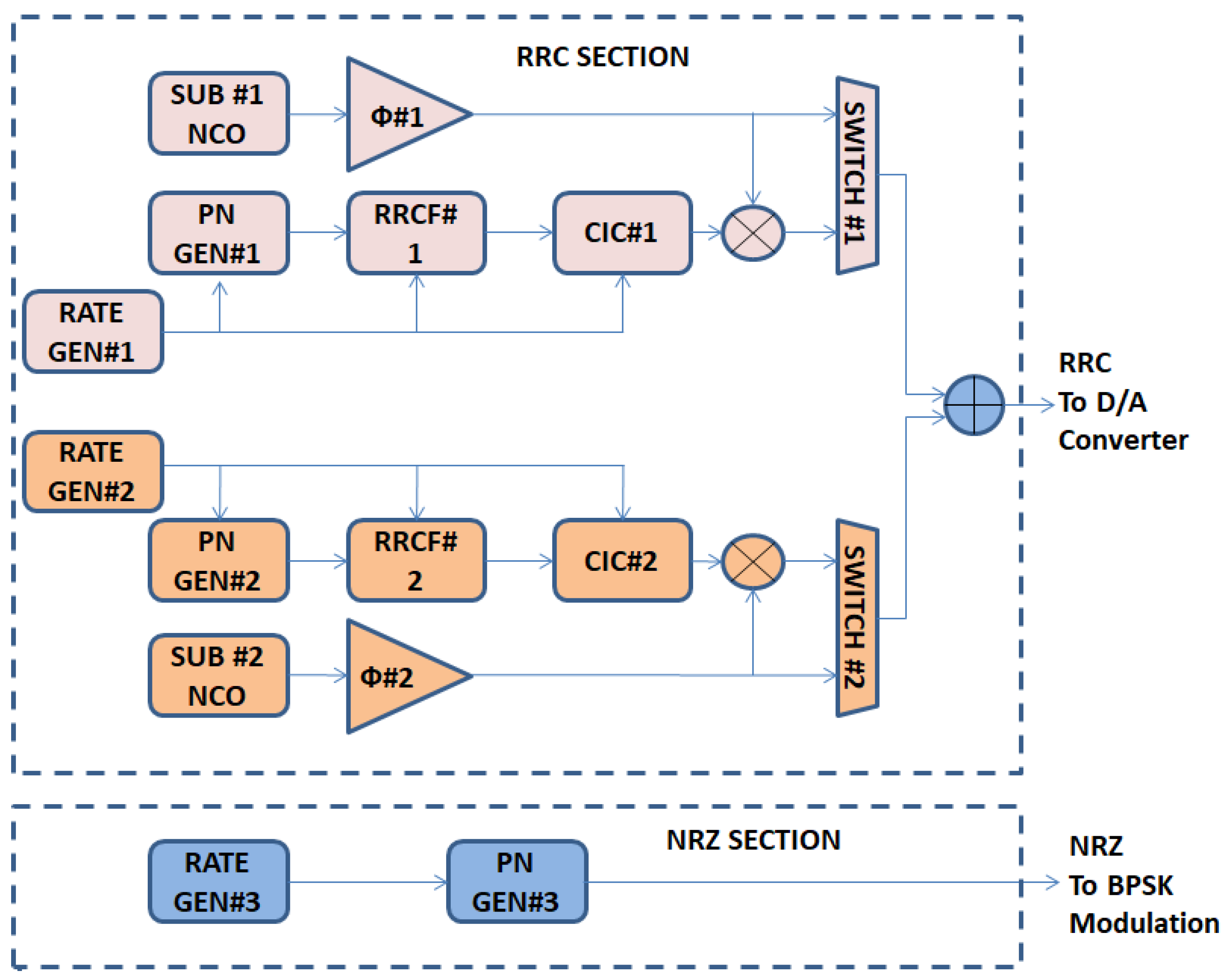
NRZ). The RRC output is interfaced with a 10-bit D/A converter connected to both the X and Ka transmission modules, while the NRZ signal feeds the Ka transmission module. The architecture of the core is detailed in
Figure 4; it consists of two sub-parts, named
RRC Section and
NRZ Section.
The proposed W-
DOR core has been designed for
with reference to Equation (
2), with one NRZ- and two RRC-shaped signal components. Hence, the RRC and NRZ sections have, respectively, two and one data paths. A detailed description of the W-
DOR core components is provided in the following subsections.
3.1.1. Rate Generator
The different sampling rates and chip rates are derived from the main clock at frequency . The Rate Generator generates two enable signals: the first one is used by the PN generator to control the output chip rate, and the second one is used to tune the sampling rate of the output section of the RRC filter and the input section of the CIC filter.
3.1.2. Pseudo Noise Generator
A set of two Linear Feedback Shift Registers (LFSRs) generates the PN sequences. The output registers are combined to obtain a Gold Code. The seeds and the generating polynomials are reconfigurable.
3.1.3. Root Raised Cosine Shaping Filter (RRCF)
This filter interpolates and shapes the incoming PN code. The coefficients are reconfigurable, the filter order is 128 and the interpolation factor is 8. It is implemented in transposed form and the polyphase decomposition (eighth order) is applied for optimizing the computational load. The resulting 136 filter coefficients (129 plus 7 null padding values) are distributed in a total of 17 memories containing each of the eight phase coefficients. No multipliers are required as the input signal is single bit, i.e., it can assume only the values (coded as 0 logic) and 1 (coded as 1 logic). The multiplication of the 12-bit coefficients is performed by multiplexers, which select the current values or the additive inverse, computed by using a radix-2 complement converter.
3.1.4. CIC Interpolation Filter
The output of the RRC Filter needs further interpolation because the chip rate is parametric. The rate change is performed by using a Comb-Interpolation-Cascaded (CIC) filter that offers several advantages:
The interpolation factor is easy to reconfigure with respect to other approaches.
The algorithm does not require multipliers.
It provides a linear phase response.
The implemented CIC filter is composed of four sections, obtaining a stop-band attenuation of 80 dB minimum. The Comb filter section registers are 12-bit wide, while the integration section registers width is 23 bit, as shown in [
14]. The filter output word length is truncated to 16 bits.
3.1.5. Subcarrier Generation
The W-DOR DSP core must generate two subcarriers at and . Two Numeric Controlled Oscillators (NCOs) are used: the phase accumulator is 32-bit wide, while the phase is truncated to 16 bits. The phase-to-amplitude conversion is performed by a 14-iteration CORDIC. Each iteration is computed in parallel to maximize the throughput. The NCO output register is 16-bit wide. Additional blocks in the RRC section are: two switches for selecting the narrowband/wideband configuration, attenuators (named #) to implement modulation indexes, multipliers to modulate the subcarriers, and an adder to mix the two waveforms.
3.2. Simulation and Synthesis Results
The W-
DOR DSP core was simulated in MATLAB & Simulink, in both floating point (FLP) and fixed point (FXP) arithmetic. A simulation-based FLP to FXP optimization flow was performed to minimize the registers word length maintaining the target specification of 50 dB of Dynamic Range on the generated RRC signal depending on the modulation index value. The W-
DOR core architecture (
Figure 2) was coded in VHDL, synthesized by using ALTERA Quartus II 13 IDE Tool, and was implemented on an ALTERA Stratix II EP2S180 FPGA. The maximum clock frequency was 137.9 MHz (100 MHz required). A summary of the hardware resources usage (post Place & Route) is shown in
Table 1.
3.3. Experimental Results
The W-
DOR bread-board is composed of a 0.18 µm ATMEL KaT ASIC (i.e., ATC18RHA family) integrated in the TAS digital transponder platform [
12,
15] and by an ALTERA FPGA Stratix II DSP development board implementing the W-
DOR core. The SRAM memories, integrated in the TAS digital transponder platform, are shared between the ATMEL KaT ASIC and the FPGA through a common address and data bus. The KaT ASIC includes the LEON2-FT microprocessor that is devoted to the W-
DOR core configuration and monitoring. The W-
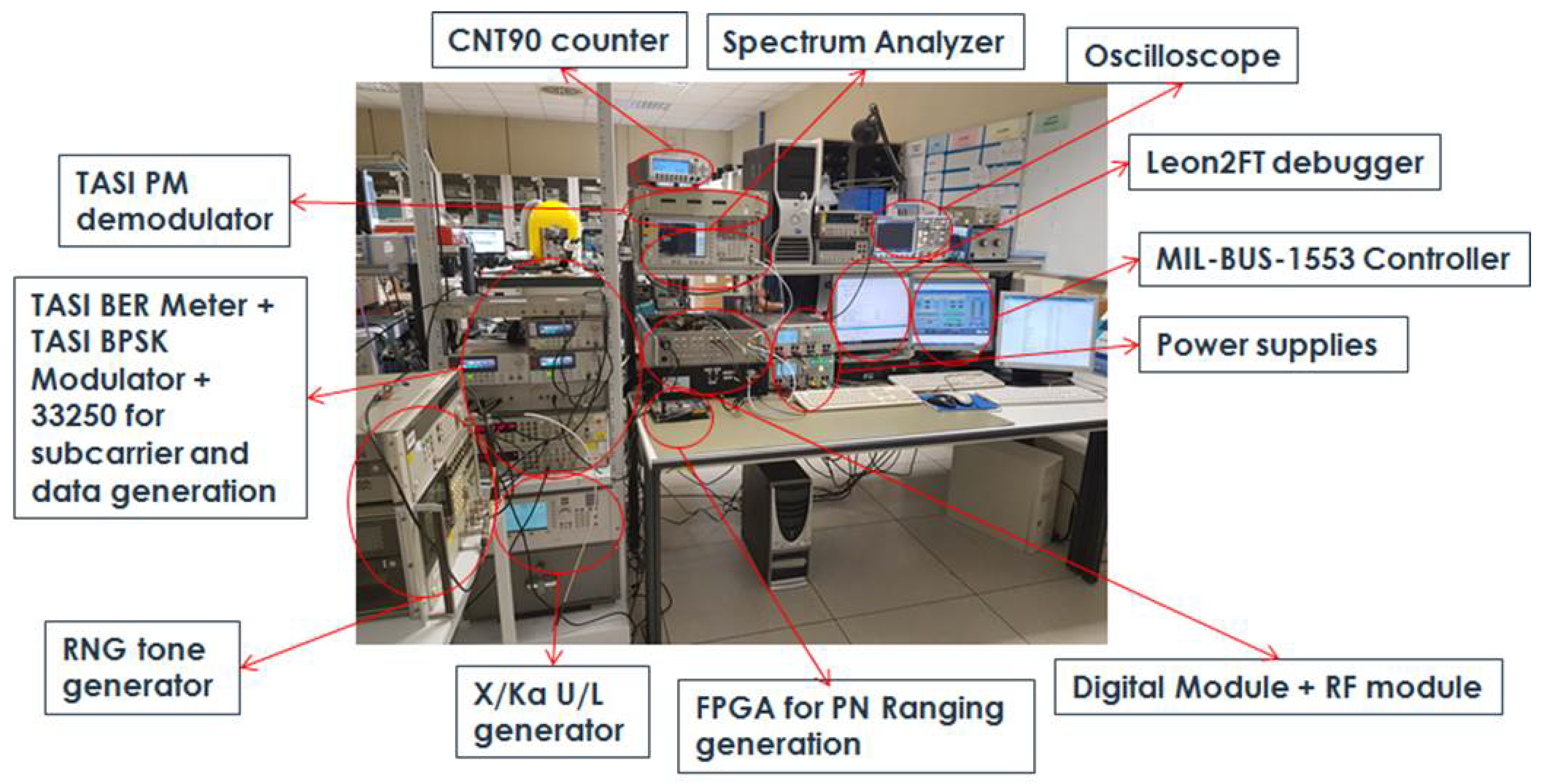
DOR signals, converted in the analog domain by the FPGA development board DAC, were characterized using a Keysight PSA E4440 spectrum analyzer (the TAS experimental setup is shown in
Figure 5).
The testbed is composed of:
FAT Digital module
RF module that includes the RX section plus the TX section
Up-link signal generation and modulation that includes:
Spectrum analyzer for spectral analysis
Leon2FT debugger
MIL-BUS-1553 Controller
CNT90 counter for Allan deviation and frequency stability measurements
FPGA Altera for W-ΔDOR signal generation
Oscilloscope
Power supplies for RF module
STD Ranging generation and demodulation that includes:
Network analyzer
TASI PM demodulator
The experiments were performed on different test cases corresponding to different sets of the configuration, provided in
Table 2.
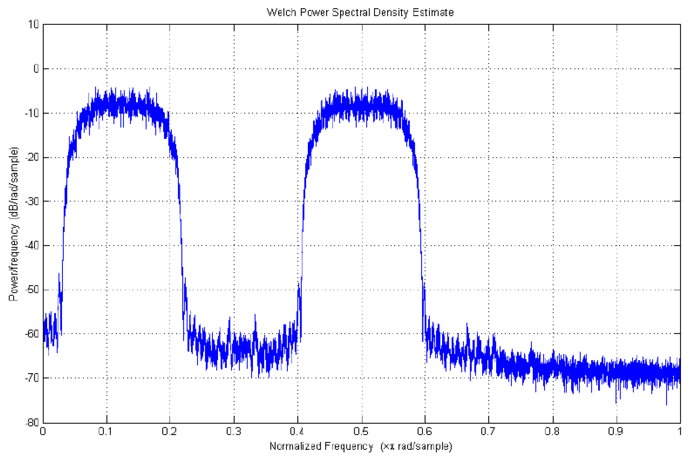
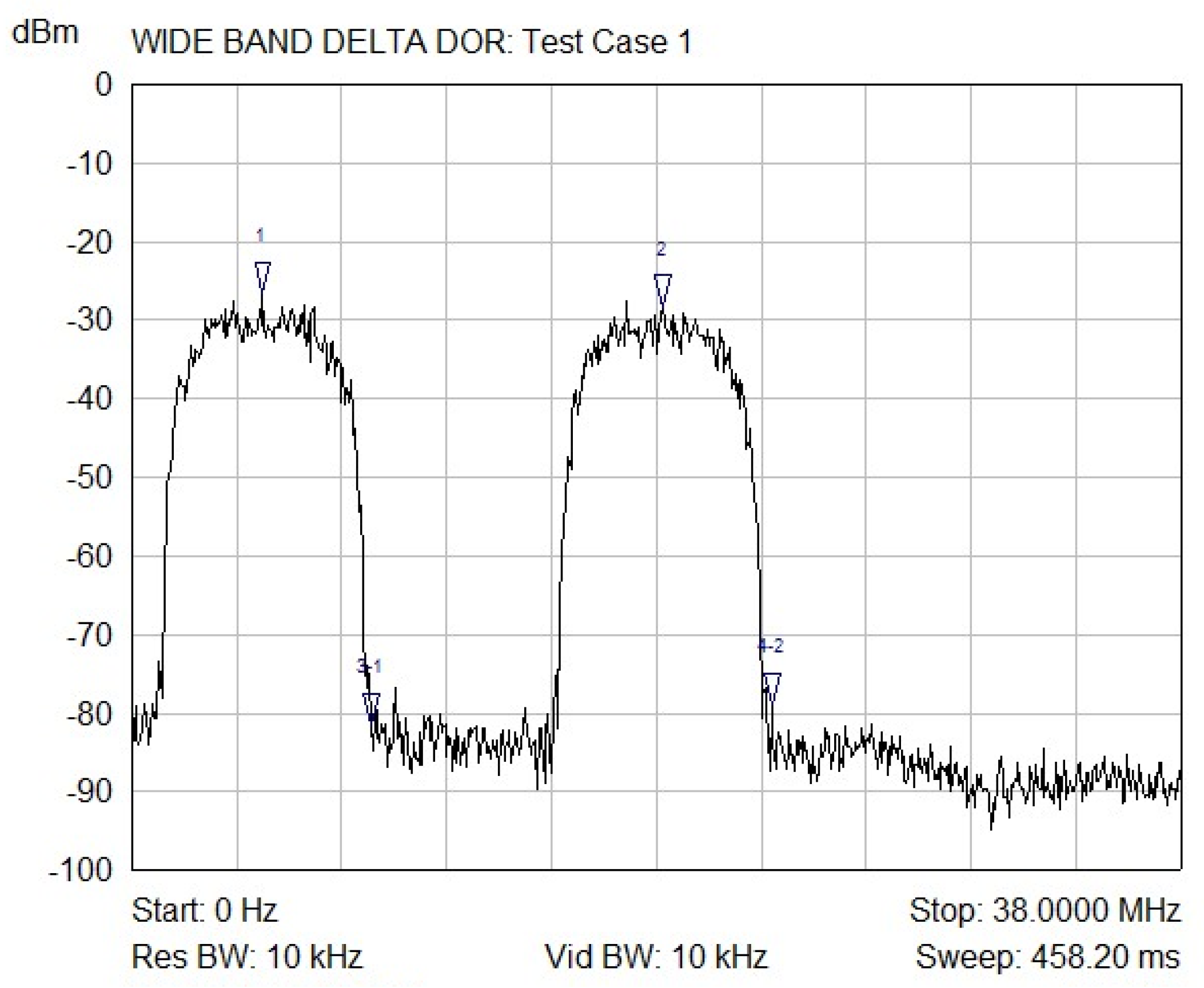
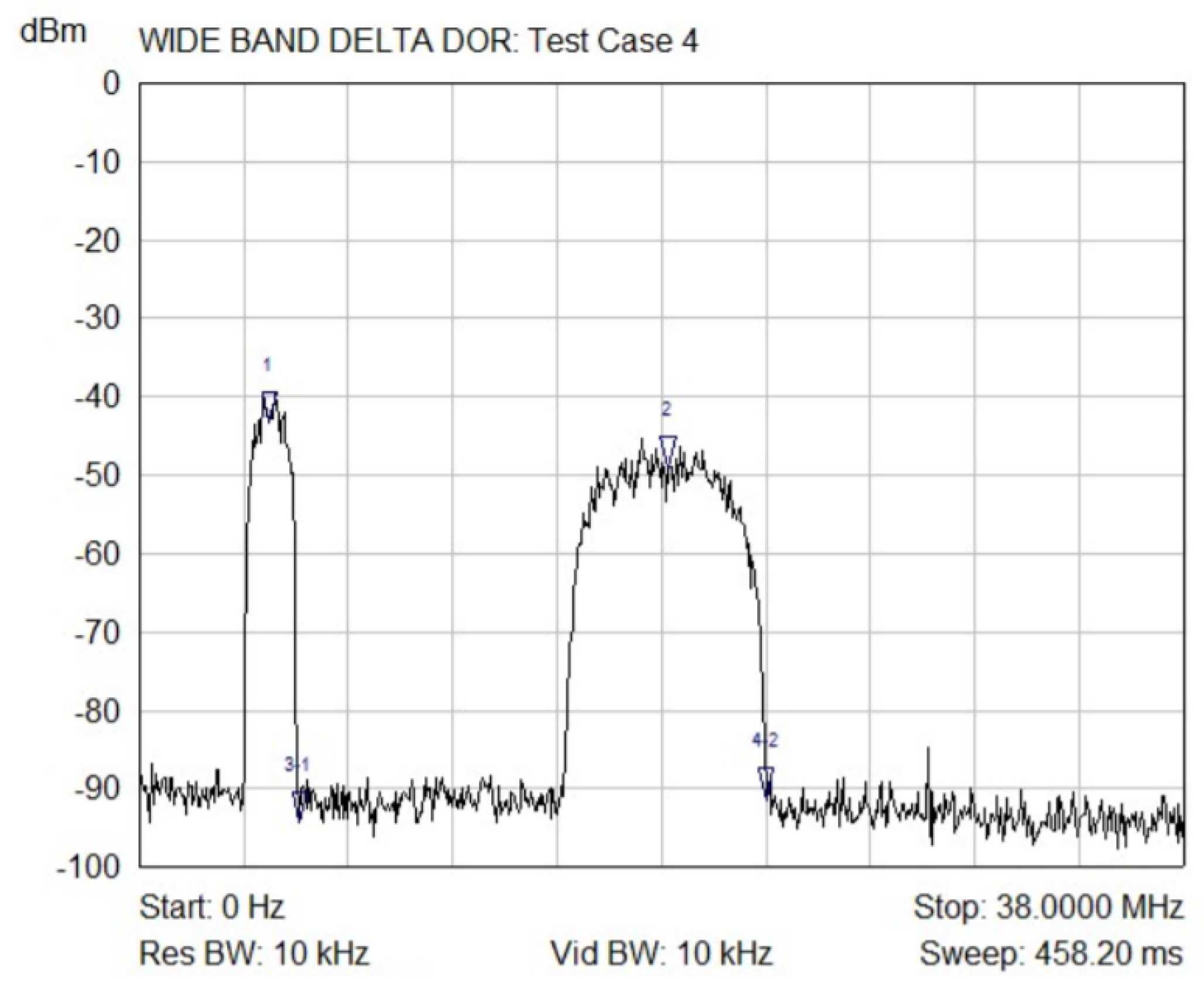
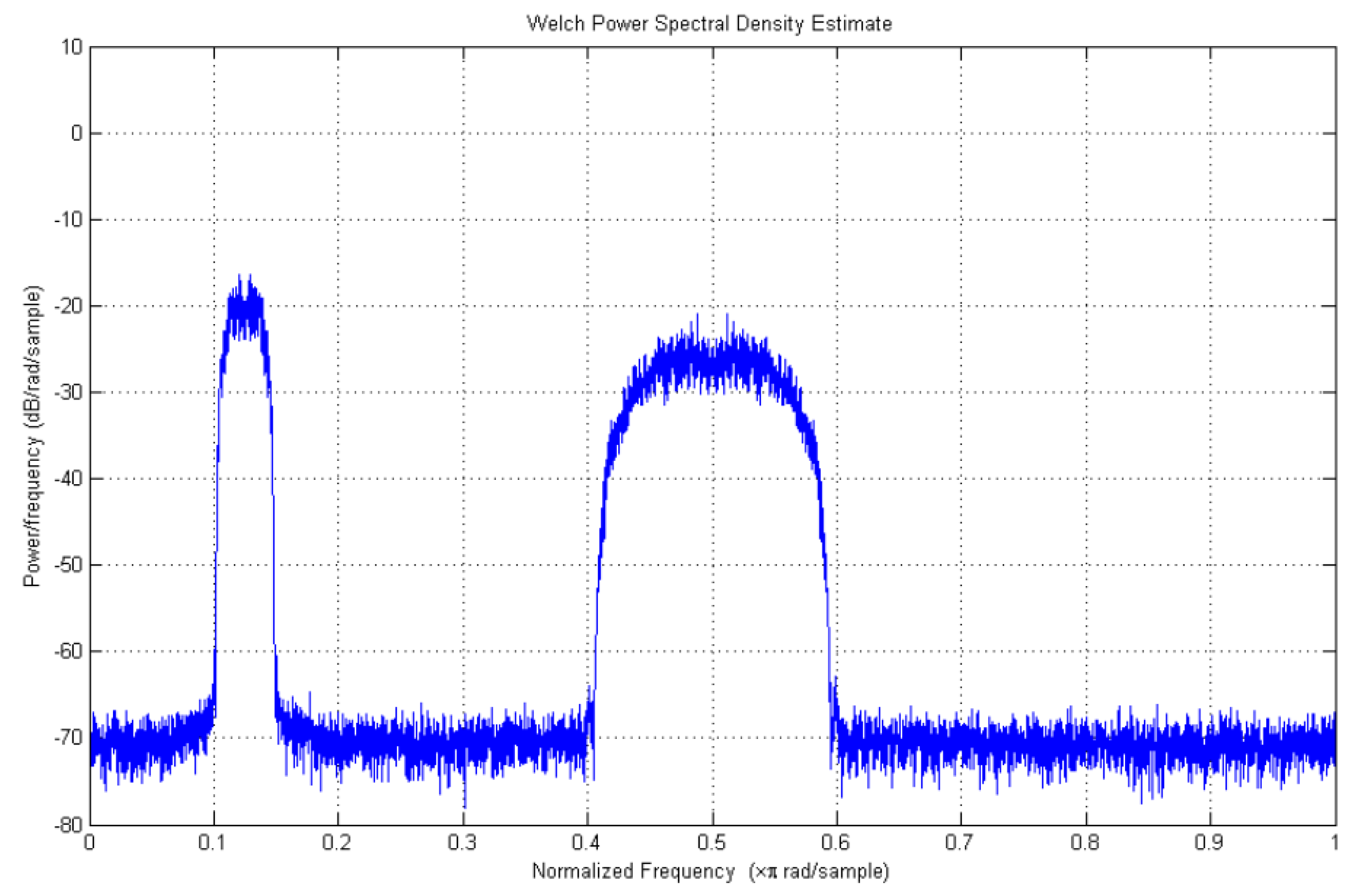
The spectra obtained by simulation and from experimental measurements, illustrated in
Figure 6 and
Figure 7 (Test Case 1) and in
Figure 8 and
Figure 9 (Test Case 4), match well, excluding a gain bias due to the digital-to-analog conversion.
In particular,
Figure 6 shows the measured output spectrum achieved with the subcarrier 1 at frequency F1/2 and subcarrier 2 at frequency 2F1, both modulated with the PN code at chip rate F1/2. In this case, the modulation index is set to 1 rad-pk. The DAC sampling frequency is about 76 MHz, thus the Nyquist window from 0 to about 38 MHz is reported. In
Figure 8, the measured output spectrum corresponding to Test Case 4 is reported. In this condition, the subcarrier 1 at frequency F1/2 is modulated by a PN code at F1/8, while the subcarrier 2 at frequency 2F1 is modulated with PN code at rate F1/2. This test also shows the ability of the W-
DOR to independently set the amplitude of each subcarrier.

 ,
, 


