Article

Enhanced Pathological Element-Based Symbolic Nodal Analysis

1
National Kaohsiung University of Science and Technology, Kaohsiung 807, Taiwan
2
Department of Electrical Engineering, Faculty of Engineering, State University of Malang, Malang 65145, Indonesia
3
Department of Physics, University of Dalat, Dalat City 670000, Vietnam
4
Graduate Institute of Clinical Medicine, Kaohsiung Medical University, Kaohsiung 807, Taiwan
*
Author to whom correspondence should be addressed.
Appl. Sci. 2019, 9(1), 93; https://doi.org/10.3390/app9010093
Submission received: 16 November 2018 / Revised: 19 December 2018 / Accepted: 22 December 2018 / Published: 27 December 2018
(This article belongs to the Special Issue Physics and Mechanics of New Materials and Their Applications)

Abstract

:
An improved symbolic analysis procedure to enhance the analytic efficiency of the reported symbolic nodal analysis is presented. Two techniques are adopted in the proposed method to reduce the order of the system of equations when performing symbolic analysis. The first one uses voltage signal sources directly to perform symbolic analysis without replacing them with their nullor equivalences. The second one uses the nullor, grounded mirror, and floating mirror elements to model the active devices that involve differential or multiple single-ended signals. Practical examples are given which demonstrate the feasibility of the proposed methods.

1. Introduction

Nullor and mirror pathological elements have been proven to be very valuable components for network analysis, synthesis and design [1,2,3,4,5,6,7,8,9,10,11,12,13]. The main reasons for the popularity of the nullor elements are their ability to model active circuits independently of the particular realization of the active devices. The symbolic circuit analysis can be carried out by only applying nodal analysis (NA). The pathological grounded voltage mirror (VM) and current mirror (CM) were defined in 1999 [14]. They can be used to represent active devices with current or voltage reversing properties in concise circuit structures compared to their nullor-equivalent counterparts. The grounded mirror (GM) elements have been further extended to include the floating mirror (FM) elements [15]. The FM elements were used to derive pathological sections to ideally represent various popular analog signal processing properties that involve differential or multiple single-ended signals. Therefore, many new active devices with such characteristics can be modeled using nullor-grounded mirror-floating mirror (NGMFM) elements in more compact forms compared with their grounded pathological equivalences [15,16,17,18,19,20,21].
The symbolic NA using RLC-grounded pathological equivalences instead of their RLC-nullor representations of circuits was presented in [20] and computational algorithm was reported in reference [21]. With a smaller number of nodal equations compared to previous method [22], it achieves a considerable reduction in the order of the system of equations and in the generation of nonzero coefficients into the nodal admittance matrix. As a result, the computational complexity during the solution of the system of equations is reduced. However, a limitation of the formulation methods in references [20,21] is that the floating pathological elements cannot be included into the formulation process. Thus the compact NGMFM equivalent circuits cannot be used for NA. Some attention had been paid to the finding of nullor-grounded mirror (NGM) equivalences of the popular active devices with differential or multiple single-ended signal properties [23] and the addition of extra equations during performing symbolic NA [24]. Nevertheless, both approaches incur the increment on the order of the built nodal admittance matrices which complicate their solution process. Besides, in all of the symbolic NA articles in literature, the voltage signal sources are replaced by their nullor equivalences before applying NA.
In this paper, a systematic analytical procedure is proposed that performs efficient NA by using lower-complexity RLC-NGMFM networks. This proposed method makes good use of the compactness of floating mirror models and treats input voltage signal source as a grounded norator to avoid using its equivalent circuit. The effect on the reduction of the order of the system of equations matrix when performing symbolic NA is demonstrated by practical examples.

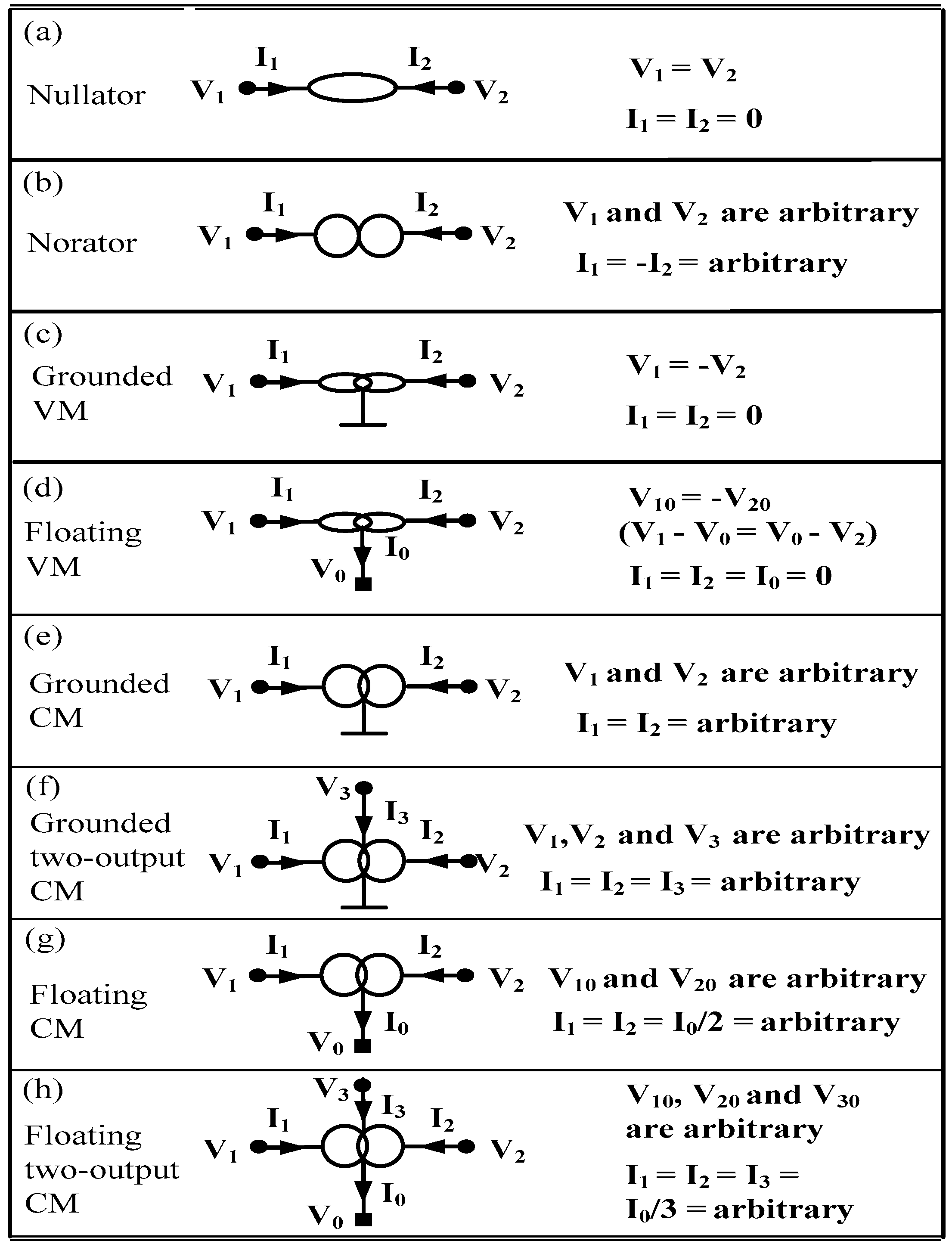
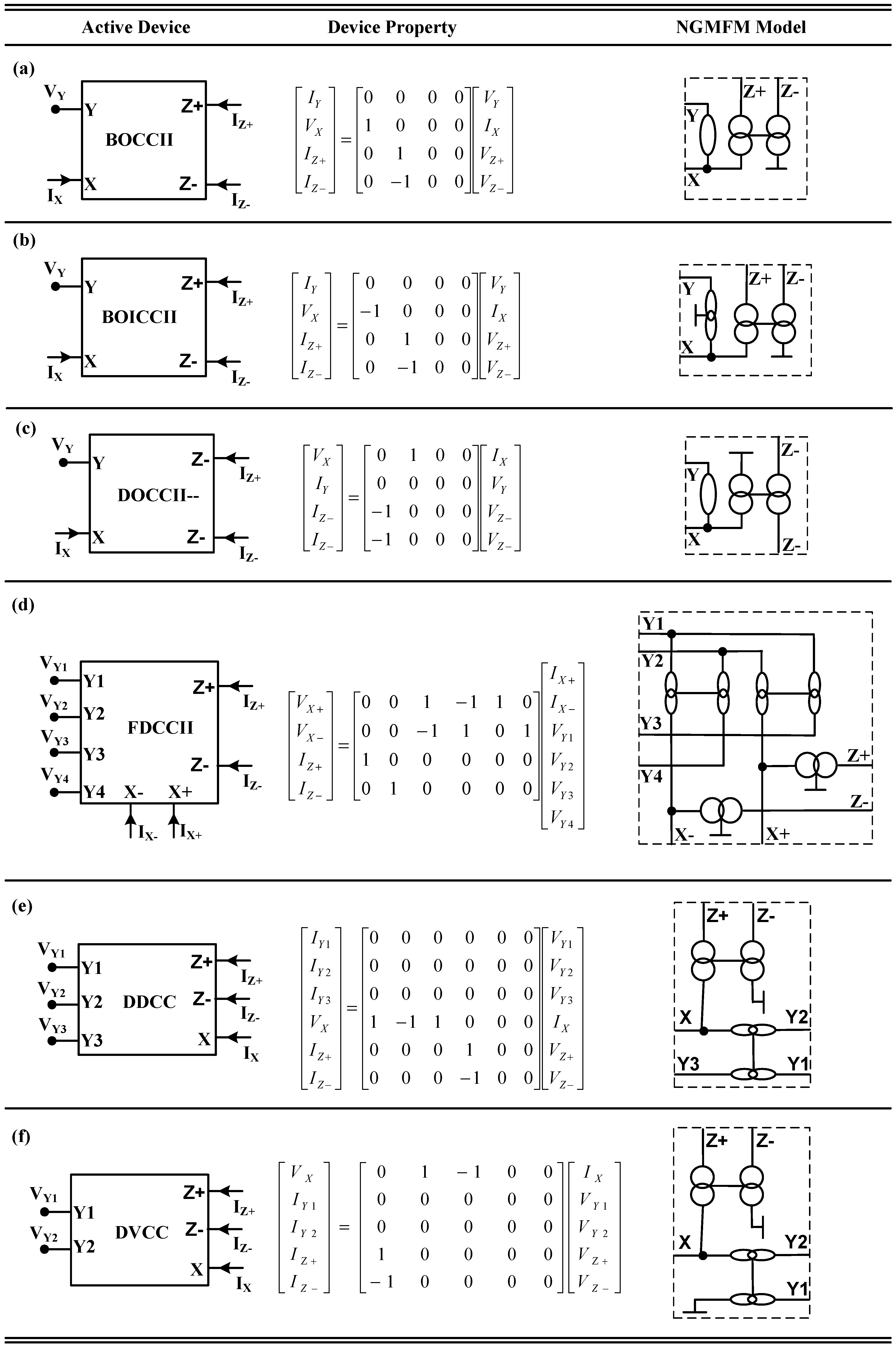
2. Pathological Section-Based Active Device Model

The definition of nullor, GM, and FM elements are shown in Figure 1. Despite the GMs being two-port network elements, they can be used as two terminal bi-directional elements with the reference node unused [10]. The GM elements in Figure 1c,e are respectively the special cases of their floating counterparts in Figure 1d,g. It can also be found that the grounded and floating two-output CMs in Figure 1f,h are simple extensions of the structures in Figure 1e,g, respectively. Figure 2 shows some pathological FM sections which represent analog signal processing properties involving differential or multiple single-ended signals. Figure 2a–d have been reported in reference [15]. The structure in Figure 2e is constructed by the floating two-output CM in Figure 1h for modeling the active devices with more current outputs. The sections in Figure 2a,b are called “floating VM sections” for the remainder of this article. The modelling of active devices using NGMFM elements was proposed in references [15,16,17]. In comparison with their representations using only nullor elements [18] or NGM elements [20,21,23], the NGMFM representations which have a smaller node count are more concise. In references [15,16,17], additional dummy pathological elements are added to the pathological representations of the balanced output second generation current conveyor (BOCCII), balanced output inverting second generation current conveyor (BOICCII), fully differential second generation current conveyor (FDCCII), double output CCII with two Z− outputs (DOCCII−), differential voltage current conveyor with a Z+ output terminal (DVCC+) and differential voltage current conveyor with a Z− output terminal (DVCC−) to constitute complete sets of pathological pairs. However, the dummy pathological elements are not needed since each unknown terminal voltage (or branch current) can be obtained from other known terminal voltage(s) (or branch current(s)) according to the element properties. Figure 3 shows the modified NGMFM models of some aforementioned active devices and differential difference current conveyor (DDCC). All voltages and currents of the terminals of the active models in Figure 3 are still uniquely and definitely determined when performing NA since they result in the same number of removed unknown variables and nodal equations by using the proposed symbolic NA method in Section 3.

3. Symbolic NA of RLC-NGMFM Network

To perform symbolic NA on the RLC–NGMFM networks, the analytic steps in reference [20] are modified as below.
Step 1:
For the symbolic NA of an arbitrary interconnection of RLC–NGMFM networks with (N + 1) nodes (excluding the reference nodes between two mirror elements since we do not particularly wish to know the voltages of these reference nodes), select a ground node and label all other nodes from 1 to N. Mark the directions of current flow through each of norators, CMs, current replication cells and input voltage signal sources to build nodal equations.
Step 2:
Write the nodal admittance equations for each labeled node in matrix form as
I = YN × N V
I = {I1, I2, …, IN}’, where the ith component Ii is defined as the sum of the currents flowing into the ith node from the independent current sources, input voltage signal sources, norators, grounded CMs, or current replication cells. YN × N is the passive nodal admittance matrix. V is the unknown column vector {V1, V2,…, VN}’ of node voltages. It must be noted that the voltage of the node connected to input voltage signal source is regarded as an unknown voltage variable in this step.
Step 3:
For a norator that is connected between nodes l and m, for example, add the equation in row m to the equation in row l and delete row m of the nodal equations. This involves adding the mth row of Y to the lth row of Y. If m is the ground node, simply delete row l of the nodal equations. The number of rows of the Y matrix is thereby reduced by one. This operation is the same as supernode. Since the characteristic of an input voltage signal source is similar to a grounded norator, the treatment of each input voltage signal source is the same as a grounded norator.
Step 4:
For a grounded CM that is connected between the nodes e and f, for example, subtract the equation in row e from the equation in row f and delete row e of the nodal equations. This involves subtracting the eth row of Y from the fth row of Y. If e is the ground node, simply delete row f of the nodal equations. A similar manipulation process can be applied to grounded two-output CM. For a grounded two-output CM connected between the nodes e, f and g (none is grounded), subtract the equation in row e from the equation in row f, and subtract the equation in row e from the equation in row g and delete row e of the nodal equations. If one of the three nodes is grounded, this grounded two-output CM can be regarded as a grounded CM connected between two ungrounded nodes. One grounded CM (or grounded two-output CM) incurs the deletion of one row of the Y matrix. This operation is based on the similar properties of a grounded CM and a norator.
Step 5:
For a nullator that is connected between the nodes p and q, for example, add the elements of column q to the elements of column p and delete column q of Y. The reason is that Vp = Vq so one unknown voltage variable can be omitted. If q is the ground node, simply delete column p of Y. The number of columns of the Y matrix is thereby reduced by one.
Step 6:
For a grounded VM that is connected between the nodes r and s, for example, subtract the elements of column s from the elements of column r and delete column s of Y. If s is the ground node, simply delete column r of Y. The number of columns of the Y matrix is thereby reduced by one. This operation is based on the similar properties of a grounded VM and a nullator.
Step 7:
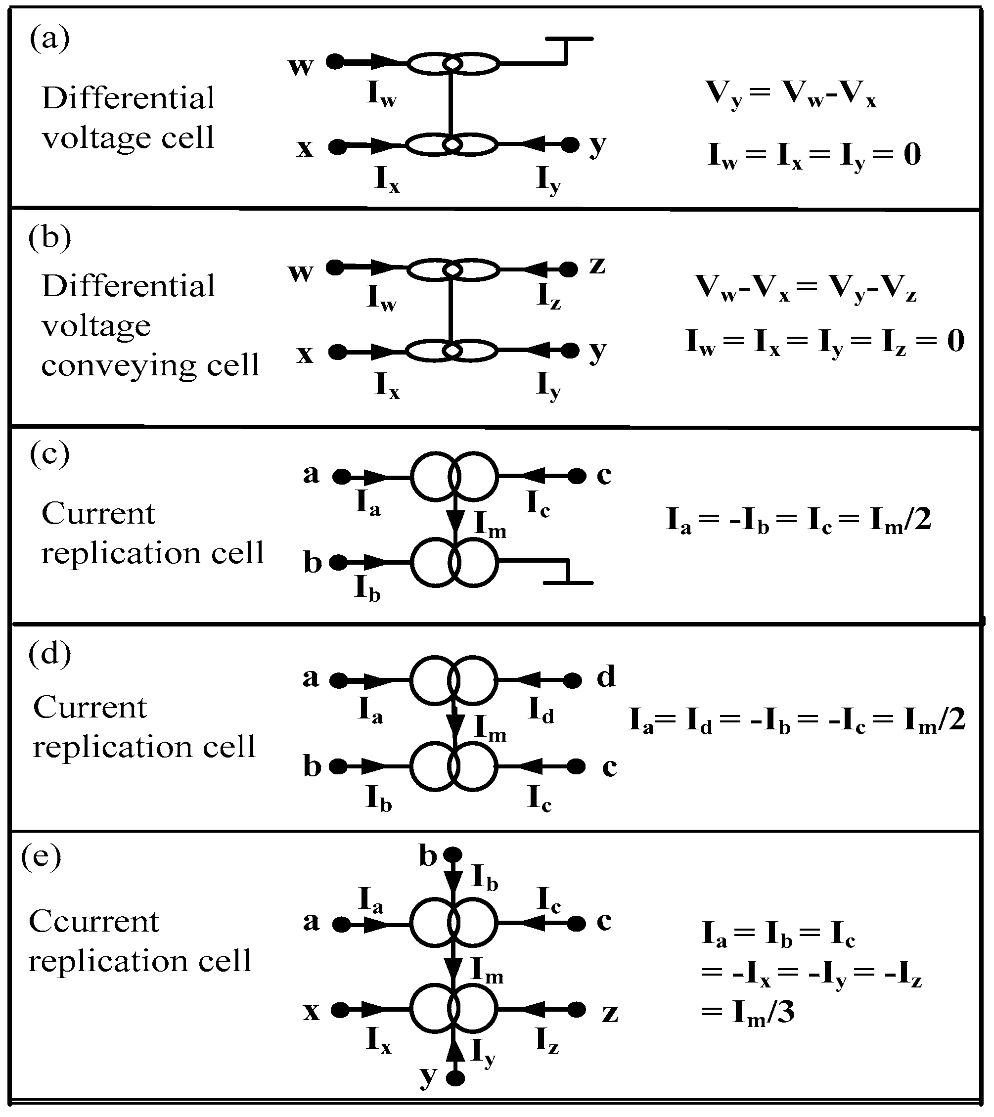
For the differential voltage conveying cell in Figure 2b that is connected between the nodes w, x, y and z terminals, select the ungrounded node w, for example, then add the elements of column w to the elements of column x, add the elements of column w to the elements of column y and subtract the elements of column w from the elements of column z and then delete column w of Y. This operation is based on the voltage property (Vw = Vx + Vy − Vz) of the differential voltage conveying cell. For the differential voltage cell in Figure 2a with voltage property (Vw = Vx + Vy), the operation is similar to a differential voltage conveying cell except the discard of column z operation. It must be noted that each of floating VM sections incur the deletion of one column of Y matrix.
Step 8:
For the pathological current replication cell in Figure 2d that is connected between the nodes a, b, c and d terminals, for example, add the equation in row a to the equation in row b, add the equation in row a to the equation in row c, subtract the equation in row a from the equation in row d and delete row a of the nodal equations. The above operation is based on the current property (Ia = Id = -Ib = -Ic) of a current replication cell. A similar manipulation process can also be applied to the current replication cells in Figure 2c,e. It must be noted that each current replication cell in Figure 2c–e will incur the deletion of one row of Y matrix.
Step 9:
Move the terms of node voltages connected to input voltage signal sources in matrix V of (1) into matrix I of (1) since they are known variables. Then a square nodal admittance matrix can be obtained. The equations can be solved to obtain a unique solution for each unknown voltage variable.

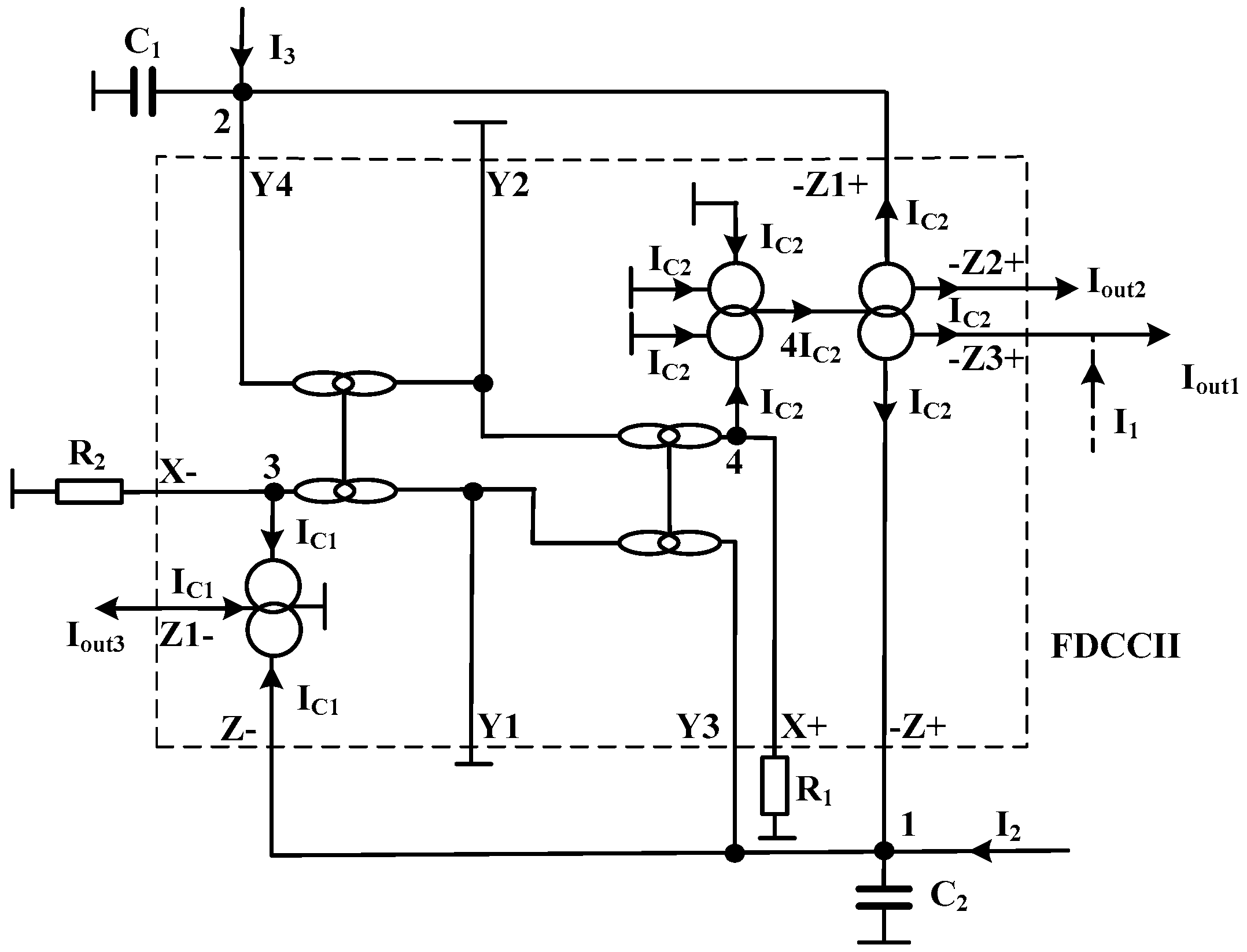
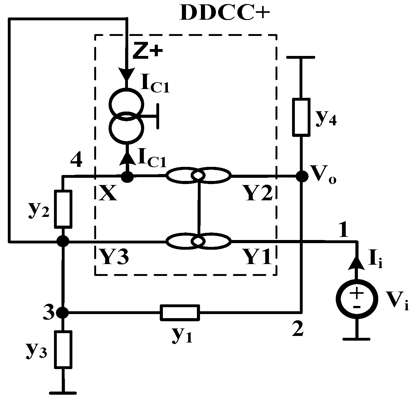
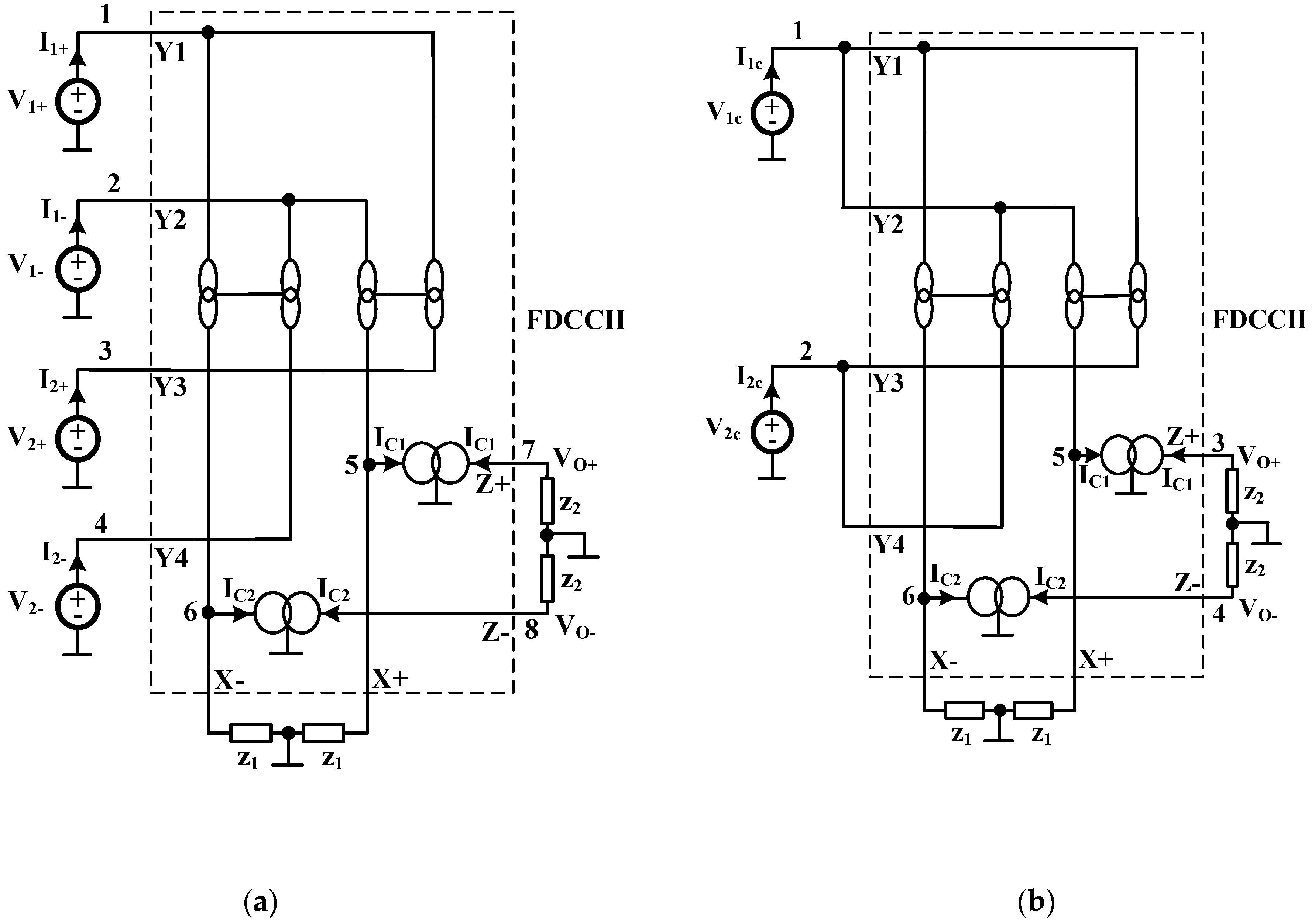
4. Application Examples

To demonstrate the usage of the presented symbolic NA method and the proposed active models, three circuit examples are given below. Considering the FDCCII-based current-mode biquad in Figure 2 of reference [25], its NGMFM equivalence is given in Figure 4. The multiple-output FDCCII model is derived from the model in Figure 3d by replacing the CMs with the grounded two-output CM in Figure 1f and the current replication cell with seven outputs (the extended version of current replication cell in Figure 2e). Based on the steps 1–2 in Section 3, the nodal admittance equations in matrix form can be obtained as:
[ I 2 + I C 2 I C 1 I 3 + I C 2 I C 1 I C 2 ] = [ s C 2 0 0 0 0 s C 1 0 0 0 0 G 2 0 0 0 0 G 1 ] [ V 1 V 2 V 3 V 4 ]
By applying the 3th to 4th steps of the proposed analytic procedure, as given by (3), one equation has been removed since one grounded two-output CM incurs the deletion of one row. Applying the 5th to 7th steps, two unknown voltage variables have been removed since each differential cell incurs the deletion of two columns of the nodal admittance matrix, as given by (4).
[ I 2 + I C 2 I 3 + I C 2 I C 2 ] = [ s C 2 0 G 2 0 0 s C 1 0 0 0 0 0 G 1 ] [ V 1 V 2 V 3 V 4 ]
[ I 2 + I C 2 I 3 + I C 2 I C 2 ] = [ s C 2 G 2 0 s C 1 G 1 0 ] [ V 1 , 4 V 2 , 3 ]
After applying the 8th step, the nodal admittance matrix equations are obtained as (5). The current replication cell in Figure 4 incurs the deletion of one equation. By solving (5), we can obtain the outputted currents as (6)–(8).
[ I 2 I 3 ] = [ s C 2 + G 1 G 2 G 1 s C 1 ] [ V 1 , 4 V 2 , 3 ]
I o u t 2 = I C 2 = G 1 V 4 = I 2 s C 1 G 1 I 3 G 1 G 2 s 2 C 1 C 2 + s C 1 G 1 + G 1 G 2
I o u t 1 = I 1 + I C 2 = I 1 G 1 V 4 = [ I 1 ( s 2 C 1 C 2 + s C 1 G 1 + G 1 G 2 ) I 2 ( s C 1 G 1 ) I 3 G 1 G 2 ] s 2 C 1 C 2 + s C 1 G 1 + G 1 G 2
I o u t 3 = I C 1 = G 2 V 3 = I 2 ( G 1 G 2 ) + I 3 ( s C 2 G 2 + G 1 G 2 ) s 2 C 1 C 2 + s C 1 G 1 + G 1 G 2
The results are in according with the expressions in Equations (10)–(12) of [25], so the validity of the proposed method is confirmed.
The second application example, which takes into account the DDCC+-based filter in Figure 2a of [26], is a voltage-mode filter. Figure 5 depicts its NGMFM equivalence using the DDCC model in Figure 3e with omission of duplicated current at Z− terminal. According to steps 1–2 in Section 3 of the proposed method, the nodal admittance equations in matrix form can be obtained as (9).
Applying steps 3 and 4 respectively incur the deletion of one equation, so (9) becomes (10). Based on steps 5–8, the nodal admittance equations can be obtained as (11) because of the voltage property (V4 = V3V2 + V1) of the DDCC+. By applying step 9, the square nodal admittance matrix can be obtained, as given by (12). Thus the transfer function is computed from (12) and given by (13). The analyzed results are consistent with the expressions in Equation (11) of [26].
[ I i 0 I C 1 I C 1 ] = [ 0 0 0 0 0 y 1 + y 4 y 1 0 0 y 1 y 1 + y 2 + y 3 y 2 0 0 y 2 y 2 ] [ V 1 V 2 V 3 V 4 ]
[ 0 0 ] = [ 0 y 1 + y 4 y 1 0 0 y 1 y 1 + 2 y 2 + y 3 2 y 2 ] [ V 1 V 2 V 3 V 4 ]
[ 0 0 ] = [ 0 y 1 + y 4 y 1 2 y 2 y 1 + 2 y 2 y 1 + y 3 ] [ V 1 V 2 V 3 ]
[ 0 2 y 2 V 1 ] = [ y 1 + y 4 y 1 y 1 + 2 y 2 y 1 + y 3 ] [ V 2 V 3 ]
V 2 V 1 = V o V i = 2 y 1 y 2 2 y 1 y 2 + y 1 y 3 + y 1 y 4 + y 3 y 4
To show the benefit of the proposed method, the formulation methods in references [18,20,23,24] are applied to the circuit in Figure 5. It can be found that both the DDCC+ equivalent nullor model in [18] and the DDCC+ equivalent NGM model in Figure 5 of reference [23] are more complicated (with a larger node count) compared to its NGMFM model. For the method in reference [24], the NGMFM active models are used. But the dimension of the admittance matrix is increased because additional equations may be added during its formulation process. Comparisons between the sizes of admittance matrix and the generation of nonzero coefficients based on different formulation methods are summarized in Table 1. We can see that by applying the formulation method described in Section 3, both the size of the admittance matrix and the count of non-zero coefficients are smaller than those generated with other formulation methods. Therefore, the proposed method achieves a more efficient symbolic NA.
The third example considers the fully differential amplifier circuit in Figure 14 of reference [27]. To calculate the differential-mode output (VOd) and common-mode output (VOc), the active device FDCCII is modeled by its NGMFM equivalent and the circuits are depicted in Figure 6a,b, respectively. The input and output voltages are defined as below.
V i d = 1 2 ( V i + V i ) V i c = 1 2 ( V i + + V i )   ( i = 1 ,   2 )
V O d = 1 2 ( V O + V O ) V O c = 1 2 ( V O + + V O )
According to Figure 6a, it is known that V1− = −V1+ and V2− = −V2+. We obtain V1d = V1+ = V1 = −V1− = −V2 and V2d = V2+ = V3 = −V2− = −V4 from (14). Based on steps 1 and 2 in Section 3, we can derive the system of equations in (8 × 8) matrix form as in (16). However, adopting the analytic method in reference [20,23], when we build the system of equations to compute the differential-mode output of the same circuit, 19 nodal admittance equations will be built. This is because each input voltage signal source is replaced by its nullor equivalence (thus additional 4 equations are added) and more complicated NGM model (there are 15 ungrounded nodes in the NGM model of FDCCII in Figure 5 of reference [23]) is used. Using the method in reference [24], the dimension of initial built the system of equations is (14 × 12) since there are 8 ungrounded nodes in the NGMFM model of FDCCII and 6 equations are added additionally.
[ I 1 + I 1 + I 2 + I 2 I C 1 I C 2 I C 1 I C 2 ] = [ 0 0 0 0 0 0 0 0 0 0 0 0 0 0 0 0 0 0 0 0 0 0 0 0 0 0 0 0 0 0 0 0 0 0 0 0 y 1 0 0 0 0 0 0 0 0 y 1 0 0 0 0 0 0 0 0 y 2 0 0 0 0 0 0 0 0 y 2 ] [ V 1 V 2 V 3 V 4 V 5 V 6 V 7 V 8 ]
By applying steps 3 and 4 in Section 3, the system of equations can be expressed as (17) since the voltage signal sources in Figure 6a are treated as grounded norators. Based on the property of differential voltage conveying cell, (namely, V5 = V1V2 + V3 and V6 = −V1 + V2 + V4) and applying steps 5–8, the system of equations (17) becomes (18). It is observed that the unknown voltage variables V5 and V6 in (17) are eliminated. After applying step 9, the matrix equations can be given by (19) since it is known that V1 = −V2 and V3 = −V4. Solving V7 and V8, we can express the differential output function (VOd) by (20).
[ 0 0 ] = [ 0 0 0 0 y 1 0 y 2 0 0 0 0 0 0 y 1 0 y 2 ] [ V 1 V 2 V 3 V 4 V 5 V 6 V 7 V 8 ]
[ 0 0 ] = [ y 1 y 1 y 1 0 y 2 0 y 1 y 1 0 y 1 0 y 2 ] [ V 1 V 2 V 3 V 4 V 7 V 8 ]
[ 2 y 1 V 1 , 2 + y 1 V 3 , 4 2 y 1 V 1 , 2 y 1 V 3 , 4 ] = [ y 2 0 0 y 2 ] [ V 7 V 8 ]
V O d = 1 2 ( V 7 V 8 ) = y 1 y 2 ( 2 V 1 , 2 + V 3 , 4 ) = y 1 y 2 ( 2 V 1 d + V 2 d )
For the circuit in Figure 6b, V1c (= V1) and V2c (= V2) are respectively the common-mode input voltage signal sources. According to steps 1–2 in Section 3 of the proposed method, we can write the (6 × 6) nodal admittance equations in matrix form as (21). But the proposed methods in references [20,23] and reference [24] will need to build 15 and 10 nodal admittance equations, respectively. According to steps 3 and 4 in Section 3, the system of equations is reduced to (22). Based on the property of the differential voltage conveying cell, (i.e., V5 = V2 and V6 = V2) and applying steps 5–8 leads to the derivation of the system of equations of (23). After applying step 9, the formulation can be given by (24). Solving V3 and V4, we can express the common-mode output function (VOc) by (25).
[ I 1 c I 2 c I C 1 I C 2 I C 1 I C 2 ] = [ 0 0 0 0 0 0 0 0 0 0 0 0 0 0 y 2 0 0 0 0 0 0 y 2 0 0 0 0 0 0 y 1 0 0 0 0 0 0 y 1 ] [ V 1 V 2 V 3 V 4 V 5 V 6 ]
[ 0 0 ] = [ 0 0 y 2 0 y 1 0 0 0 0 y 2 0 y 1 ] [ V 1 V 2 V 3 V 4 V 5 V 6 ]
[ 0 0 ] = [ 0 y 1 y 2 0 0 y 1 0 y 2 ] [ V 1 V 2 V 3 V 4 ]
[ y 1 V 2 y 1 V 2 ] = [ y 2 0 0 y 2 ] [ V 3 V 4 ]
V O c = 1 2 ( V O + + V O ) = 1 2 ( V 3 + V 4 ) = y 1 y 2 V 2 = y 1 y 2 V 2 c
The analyzed results of differential output function (VOd) and common-mode output function (VOc) are in accordance with the functions given by (39) and (40) of reference [27], respectively.

5. Conclusions

In this paper, an improved formulation method with two techniques to enhance the efficiency of symbolic NA is presented. Both techniques are conducive to building smaller number of nodal equations when performing symbolic nodal analysis. It is especially practical when applied to popular high-noise-immunity circuits with differential voltage signal inputs. The proposed analytical procedure is expected to be realized in computer programs since it involves simple entries operations in matrix. Thus it is helpful in enhancing the efficiency of symbolic NA in analog design automation.

Author Contributions

Conceptualization, S. and Y.-L.L.; methodology, S. and H.-D.T.; theoretical verification, C.C.P. and H.-Y.W.; writing, review and editing, H.-Y.W. and S.-H.C.; project administration, S., H.-Y.W. and S.-H.C.; funding acquisition, H.-Y.W. and S.-H.C.

Funding

This research was funded by the Ministry of Research, Technology and Higher Education of the Republic of Indonesia (Grant No. 124.14/E4.4/2014, 7 July 2014) and the Ministry of Science and Technology of the Republic of China, grant number MOST 105-2923-E-992-302-MY3 and 107-2622-8-992-301-TE2.

Acknowledgments

The software and technical support from the Chip Implementation Center is gratefully acknowledged.

Conflicts of Interest

The authors declare no conflict of interest.

References

  1. Tellegen, B.D.H. La recherche pour una série complète d’éléments de circuit ideaux nonlinéaires. Rend. Semin. Mat. Fis. Milano 1954, 25, 134–144. [Google Scholar] [CrossRef]
  2. Carlosena, A.; Moschytz, G.S. Nullators and norators in voltage to current mode transformations. Int. J. Circuit Theory Appl. 1993, 21, 421–424. [Google Scholar] [CrossRef]
  3. Kumar, P.; Senani, R. Bibliography on nullors and their applications in circuit analysis, synthesis and design. Anal. Integr. Circuits Signal Process. 2002, 33, 65–76. [Google Scholar] [CrossRef]
  4. Swamy, M.N.S. Transpose of a multiterminal element and applications. IEEE Trans. Circuits Syst. II 2010, 57, 696–700. [Google Scholar] [CrossRef]
  5. Mitra, S.K. Equivalent circuit of gyrators. Electron. Lett. 1967, 3, 333–334. [Google Scholar] [CrossRef]
  6. Mitra, S.K. Non-reciprocal negative impedance inverter. Electron. Lett. 1967, 3, 388. [Google Scholar] [CrossRef]
  7. Hashemian, R. Fixator-norator pairs vs direct analytical tools in performing analog circuit designs. IEEE Trans. Circuits Syst. II Exp. Briefs 2014, 61, 569–573. [Google Scholar] [CrossRef]
  8. Papazoglou, C.A.; Karybakas, C.A. A transformation to obtain CCII-based adjoint of op.-amp.-based circuits. IEEE Trans. Circuits Syst. II 1998, 45, 894–898. [Google Scholar] [CrossRef]
  9. Svoboda, J.A. Using nullors to analyse linear networks. Int. J. Circuit Theory Appl. 1986, 14, 169–180. [Google Scholar] [CrossRef]
  10. Soliman, A.M. The inverting second generation current conveyors as universal building blocks. AEU Int. J. Electron. Commun. 2008, 62, 114–121. [Google Scholar] [CrossRef]
  11. Leuciuc, A. Using nullors for realisation of inverse transfer functions and characteristics. Electron. Lett. 1997, 33, 949–951. [Google Scholar] [CrossRef]
  12. Floberg, H. Symbolic Analysis in Analog Integrated Circuit Design; Kluwer Academic: Boston, MA, USA, 1997. [Google Scholar]
  13. Chipipop, B.; Surakampontorn, W. Realisation of current-mode FTFN-based inverse filter. Electron. Lett. 1999, 35, 690–692. [Google Scholar] [CrossRef]
  14. Awad, I.A.; Soliman, A.M. Inverting second generation current conveyors: The missing building blocks, CMOS realizations and applications. Int. J. Electron. 1999, 86, 413–432. [Google Scholar] [CrossRef]
  15. Saad, R.A.; Soliman, A.M. A new approach for using the pathological mirror elements in the ideal representation of active devices. Int. J. Circuit Theory Appl. 2010, 38, 148–178. [Google Scholar] [CrossRef]
  16. Soliman, A.M. On the DVCC and the BOCCII as adjoint elements. J. Circuits Syst. Comput. 2009, 18, 1017–1032. [Google Scholar] [CrossRef]
  17. Soliman, A.M. Pathological representation of the two-output CCII and ICCII family and application. Int. J. Circuit Theory Appl. 2011, 39, 589–606. [Google Scholar] [CrossRef]
  18. Huang, W.C.; Wang, H.Y.; Cheng, P.S.; Lin, Y.C. Nullor equivalents of active devices for symbolic circuit analysis. Circuits Syst. Signal Process. 2012, 31, 865–875. [Google Scholar] [CrossRef]
  19. Tan, L.; Liu, K.; Bai, Y.; Teng, J. Construction of CDBA and CDTA behavioral models and the applications in symbolic circuit analysis. Anal. Integr. Circuits Signal Process. 2013, 75, 517–523. [Google Scholar] [CrossRef]
  20. Wang, H.Y.; Huang, W.C.; Chiang, N.H. Symbolic nodal analysis of circuits using pathological elements. IEEE Trans. Circuits Syst. II 2010, 57, 874–877. [Google Scholar] [CrossRef]
  21. Sanchez-Lopez, C.; Fernandez, F.V.; Tlelo-Cuautle, E.; Tan, S.X.D. Pathological element-based active device models and their application to symbolic analysis. IEEE Trans. Circuits Syst. I 2011, 58, 1382–1395. [Google Scholar] [CrossRef]
  22. Davies, A.C. Matrix analysis of networks containing nullators and norators. Electron. Lett. 1966, 2, 48–49. [Google Scholar] [CrossRef]
  23. Sanchez-Lopez, C. Pathological equivalents of fully-differential active devices for symbolic nodal analysis. IEEE Trans. Circuits Syst. I 2013, 60, 603–615. [Google Scholar] [CrossRef]
  24. Wang, H.Y.; Chang, S.H.; Chiang, N.H.; Nguyen, Q.M. Symbolic analysis using floating pathological elements. In Genetic and Evolutionary Computing; Springer: Cham, Switzerland, 2013; pp. 379–387. [Google Scholar]
  25. Chang, C.M.; Al-Hashimi, B.M.; Wang, C.L.; Hung, C.W. Single fully differential current conveyor biquad filters. IEE Proc. Circuits Devices Syst. 2003, 150, 394–398. [Google Scholar] [CrossRef]
  26. Ibrahim, M.A.; Kuntman, H.; Cicekoglu, O. New second-order low-pass, high-pass and band-pass filters employing minimum number of active and passive elements. In Proceedings of the International Symposium on Signals, Circuits and Systems, Iasi, Romania, 10–11 July 2003; pp. 557–560. [Google Scholar]
  27. El-Adawy, A.A.; Soliman, A.M.; Elwan, H.O. A novel fully differential current conveyor and applications for analog VLSI. IEEE Trans. Circuits Syst. II 2000, 47, 306–313. [Google Scholar] [CrossRef]
Figure 1. Symbols and definitions of nullor and mirror elements.
Applsci 09 00093 g001
Figure 2. FM sections and their characteristics.
Applsci 09 00093 g002
Figure 3. Symbol and NGMFM models of some active devices.
Applsci 09 00093 g003
Figure 4. FDCCII-based current-mode biquad in Figure 2 of [23].
Applsci 09 00093 g004
Figure 5. DDCC+-based voltage-mode filter in Figure 2(a) of [24].
Applsci 09 00093 g005
Figure 6. Pathological equivalent circuit of fully differential amplifier in Figure 14 of [27] for computing (a) Differential-mode output (b) Common-mode output.
Applsci 09 00093 g006
Table 1. Comparison of different formulation methods.
Formulation MethodAdmittance Matrix SizeNon-Zero Coefficients
Symbolic NA using NGM model [18]5 × 513
Symbolic NA using NGM model [20,23]5 × 514
Symbolic NA using NGMFM model [24]4 × 410
Proposed method using NGMFM model2 × 24

