Enhanced Internal Quantum Efficiency of Bandgap-Engineered Green W-Shaped Quantum Well Light-Emitting Diode

 ,
,
Abstract
Featured Application
Abstract
1. Introduction
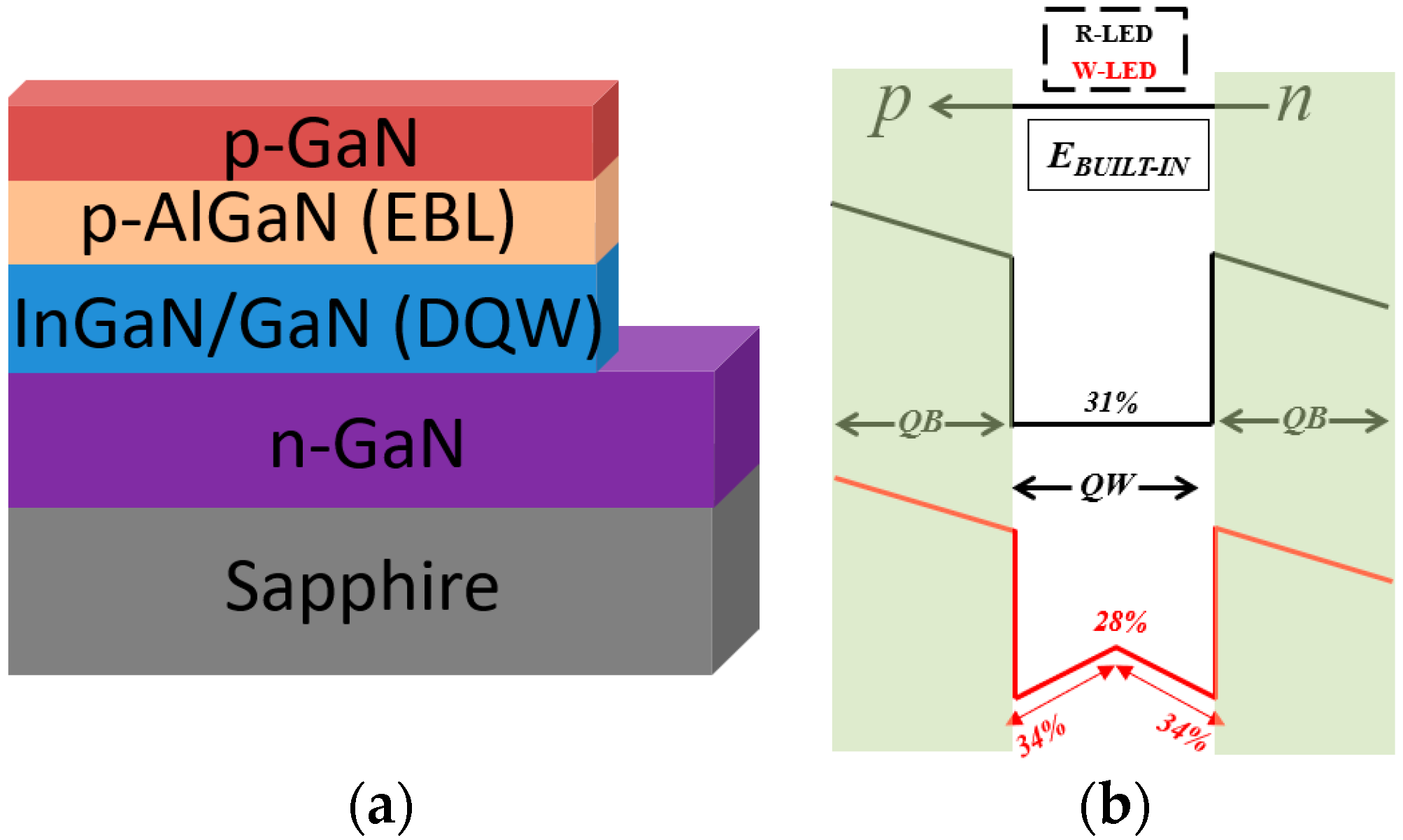
2. Device Structure
3. Methodology
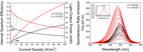
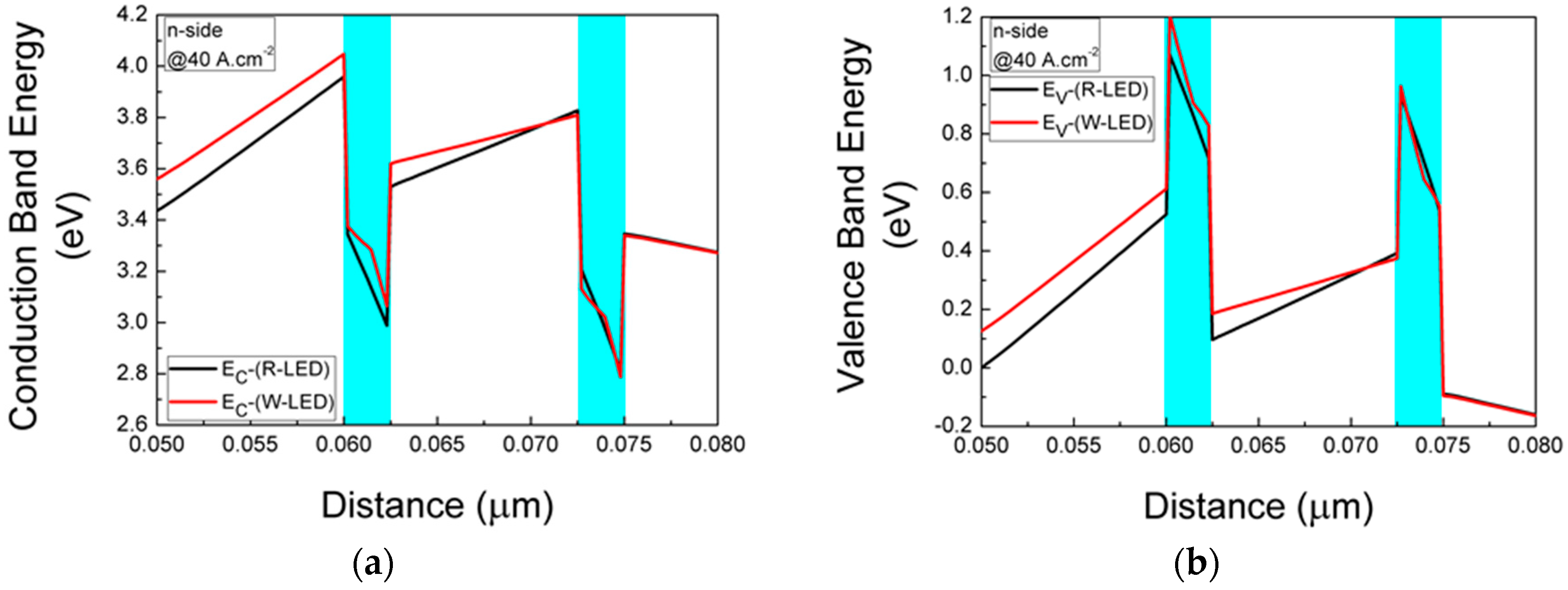
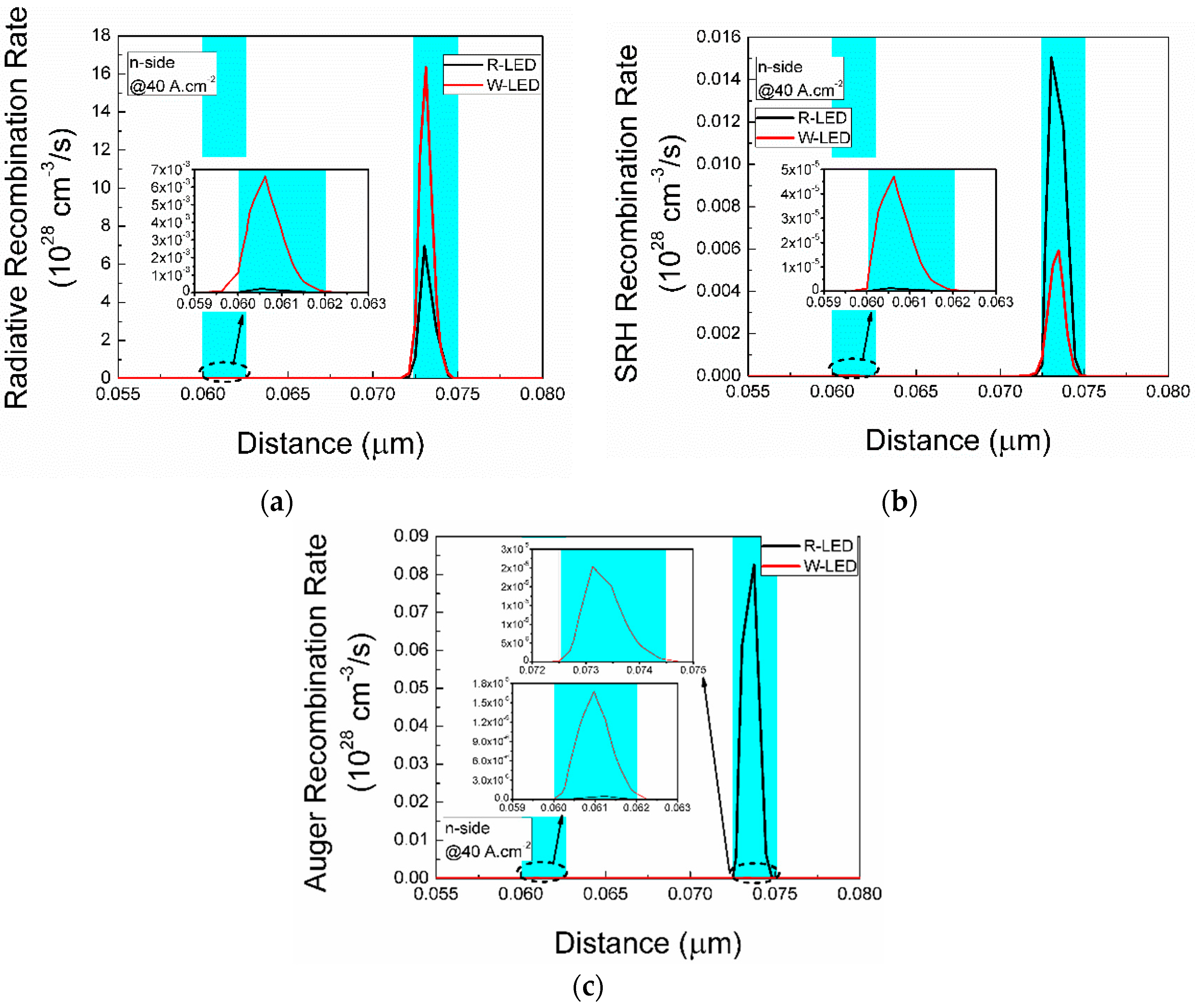
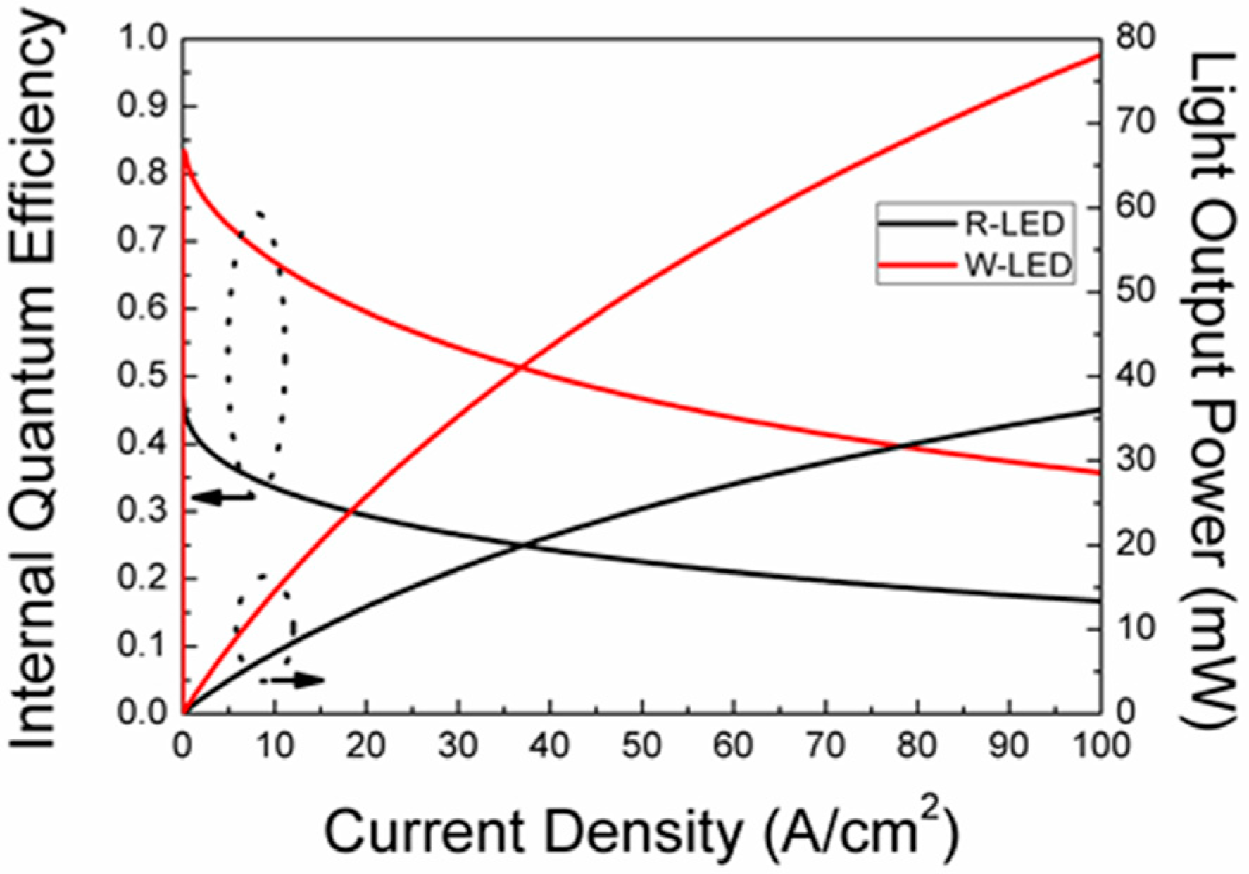
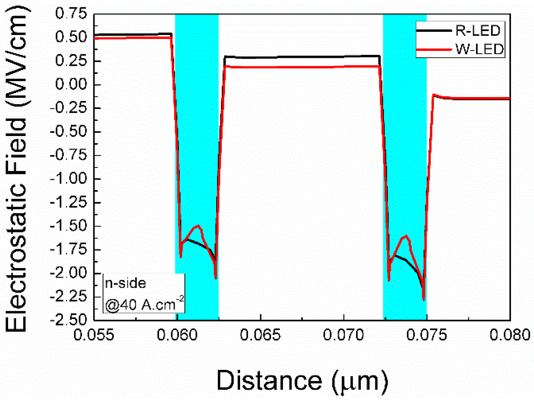
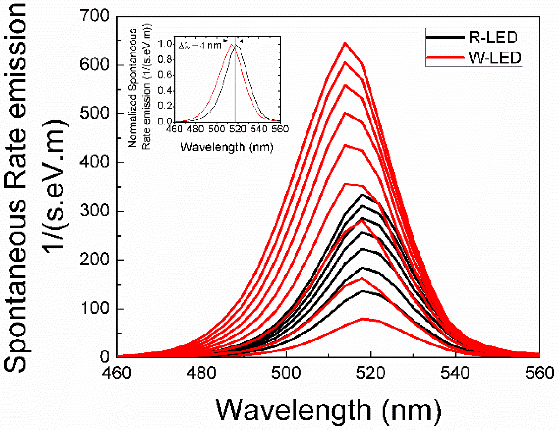
4. Results and Discussion
5. Conclusions
Author Contributions
Funding
Acknowledgments
Conflicts of Interest
References
- Crawford, M.H. LEDs for solid-state lighting: Performance challenges and recent advances. IEEE J. Sel. Top. Quantum Electron. 2009, 15, 1028–1040. [Google Scholar] [CrossRef]
- Cho, J.; Schubert, E.F.; Kim, J.K. Efficiency droop in light-emitting diodes: Challenges and countermeasures. Laser Photonics Rev. 2013, 7, 408–421. [Google Scholar] [CrossRef]
- Weisbuch, C.; Piccardo, M.; Martinelli, L.; Iveland, J.; Peretti, J.; Speck, J.S. The efficiency challenge of nitride light-emitting diodes for lighting. Phys. Status Solidi A 2015, 212, 899–913. [Google Scholar] [CrossRef]
- Farrell, R.; Young, E.; Wu, F.; DenBaars, S.; Speck, J. Materials and growth issues for high-performance nonpolar and semipolar light-emitting devices. Semicond. Sci. Technol. 2012, 27, 024001. [Google Scholar] [CrossRef]
- Ling, S.-C.; Lu, T.-C.; Chang, S.-P.; Chen, J.-R.; Kuo, H.-C.; Wang, S.-C. Low efficiency droop in blue-green m-plane InGaN/GaN light emitting diodes. Appl. Phys. Lett. 2010, 96, 231101. [Google Scholar] [CrossRef]
- Zhao, H.; Liu, G.; Zhang, J.; Poplawsky, J.D.; Dierolf, V.; Tansu, N. Approaches for high internal quantum efficiency green InGaN light-emitting diodes with large overlap quantum wells. Opt. Express 2011, 19, A991–A1007. [Google Scholar] [CrossRef]
- der Maur, M.A.; Lorenz, K.; Di Carlo, A. Band gap engineering approaches to increase InGaN/GaN LED efficiency. Opt. Quantum Electron. 2012, 44, 83–88. [Google Scholar] [CrossRef]
- Zhu, L.-H.; Liu, W.; Zeng, F.-M.; Gao, Y.-L.; Liu, B.-L.; Lu, Y.-J.; Chen, Z. Efficiency droop improvement in InGaN/GaN light-emitting diodes by graded-composition multiple quantum wells. IEEE Photonics J. 2013, 5, 8200208. [Google Scholar]
- Islam, M.; Usman, M.; Mushtaq, U.; Nawaz, N.; Karimov, K.; Muhammad, N.; Saba, K. Numerical analysis of the indium compositional variation on the efficiency droop of the GaN-based light-emitting diodes. In Proceedings of the SPIE Optical Engineering + Applications, San Diego, CA, USA, 19–23 August 2018; p. 5. [Google Scholar]
- Gerber, D.; Droopad, R.; Maracas, G. Comparison of electroabsorption in asymmetric triangular and rectangular GaAs/AlxGa1−x as multiple quantum wells. Appl. Phys. Lett. 1993, 62, 525–527. [Google Scholar] [CrossRef]
- Choi, R.; Hahn, Y.; Shim, H.; Han, M.; Suh, E.; Lee, H. Efficient blue light-emitting diodes with InGaN/GaN triangular shaped multiple quantum wells. Appl. Phys. Lett. 2003, 82, 2764–2766. [Google Scholar] [CrossRef]
- Zhao, H.; Arif, R.A.; Tansu, N. Design analysis of staggered InGaN quantum wells light-emitting diodes at 500–540 nm. IEEE J. Sel. Top. Quantum Electron. 2009, 15, 1104–1114. [Google Scholar] [CrossRef]
- Chang, C.-Y.; Li, H.; Lu, T.-C. High efficiency InGaN/GaN light emitting diodes with asymmetric triangular multiple quantum wells. Appl. Phys. Lett. 2014, 104, 091111. [Google Scholar] [CrossRef]
- Chen, J.-R.; Ling, S.-C.; Huang, H.-M.; Su, P.-Y.; Ko, T.-S.; Lu, T.-C.; Kuo, H.-C.; Kuo, Y.-K.; Wang, S.-C. Numerical study of optical properties of InGaN multi-quantum-well laser diodes with polarization-matched AlInGaN barrier layers. Appl. Phys. B 2009, 95, 145–153. [Google Scholar] [CrossRef]
- Schubert, M.F.; Xu, J.; Kim, J.K.; Schubert, E.F.; Kim, M.H.; Yoon, S.; Lee, S.M.; Sone, C.; Sakong, T.; Park, Y. Polarization-matched Ga in N/Al Ga in N multi-quantum-well light-emitting diodes with reduced efficiency droop. Appl. Phys. Lett. 2008, 93, 041102. [Google Scholar] [CrossRef]
- Wang, T.-H.; Xu, J.-L. Advantage of InGaN-based light-emitting diodes using AlGaInN electron blocking layer coupled with inserting InGaN layer. Opt. Int. J. Light Electron. Opt. 2013, 124, 5866–5870. [Google Scholar] [CrossRef]
- Kuo, Y.-K.; Chang, J.-Y.; Tsai, M.-C. Enhancement in hole-injection efficiency of blue InGaN light-emitting diodes from reduced polarization by some specific designs for the electron blocking layer. Opt. Lett. 2010, 35, 3285–3287. [Google Scholar] [CrossRef] [PubMed]
- Chung, R.B.; Han, C.; Pan, C.-C.; Pfaff, N.; Speck, J.S.; DenBaars, S.P.; Nakamura, S. The reduction of efficiency droop by Al0. 82In0. 18N/GaN superlattice electron blocking layer in (0001) oriented GaN-based light emitting diodes. Appl. Phys. Lett. 2012, 101, 131113. [Google Scholar] [CrossRef]
- Kuo, Y.-K.; Chang, J.-Y.; Tsai, M.-C.; Yen, S.-H. Advantages of blue InGaN multiple-quantum well light-emitting diodes with InGaN barriers. Appl. Phys. Lett. 2009, 95, 011116. [Google Scholar] [CrossRef]
- Xie, J.; Ni, X.; Fan, Q.; Shimada, R.; Özgür, Ü.; Morkoç, H. On the efficiency droop in InGaN multiple quantum well blue light emitting diodes and its reduction with p-doped quantum well barriers. Appl. Phys. Lett. 2008, 93, 121107. [Google Scholar] [CrossRef]
- Xiong, J.-Y.; Xu, Y.-Q.; Zheng, S.-W.; Zhao, F.; Ding, B.-B.; Song, J.-J.; Yu, X.-P.; Zhang, T.; Fan, G.-H. Advantages of GaN based light-emitting diodes with p-AlGaN/InGaN superlattice last quantum barrier. Opt. Commun. 2014, 312, 85–88. [Google Scholar] [CrossRef]
- Ni, X.; Fan, Q.; Shimada, R.; Özgür, Ü.; Morkoç, H. Reduction of efficiency droop in InGaN light emitting diodes by coupled quantum wells. Appl. Phys. Lett. 2008, 93, 171113. [Google Scholar] [CrossRef]
- Usman, M.; Saba, K.; Han, D.-P.; Muhammad, N. Efficiency improvement of green light-emitting diodes by employing all-quaternary active region and electron-blocking layer. Superlattices Microstruct. 2018, 113, 585–591. [Google Scholar] [CrossRef]
- Usman, M.; Mushtaq, U.; Saba, K.; Han, D.-P.; Muhammad, N.; Imtiaz, W.A.; Jahangir, A. Improved optoelectronic performance of green light-emitting diodes by employing GaAlInN quantum wells without electron blocking layer. Phys. E Low-Dimens. Syst. Nanostruct. 2019, 106, 68–72. [Google Scholar] [CrossRef]
- Arif, R.A.; Ee, Y.K.; Tansu, N. Nanostructure engineering of staggered InGaN quantum wells light emitting diodes emitting at 420–510 nm. Phys. Status Solidi A 2008, 205, 96–100. [Google Scholar] [CrossRef]
- Park, S.-H.; Ahn, D.; Koo, B.-H.; Kim, J.-W. Dip-shaped InGaN/GaN quantum-well light-emitting diodes with high efficiency. Appl. Phys. Lett. 2009, 95, 063507. [Google Scholar] [CrossRef]
- Han, S.-H.; Lee, D.-Y.; Shim, H.-W.; Kim, G.-C.; Kim, Y.S.; Kim, S.-T.; Lee, S.-J.; Cho, C.-Y.; Park, S.-J. Improvement of efficiency droop in InGaN/GaN multiple quantum well light-emitting diodes with trapezoidal wells. J. Phys. D Appl. Phys. 2010, 43, 354004. [Google Scholar] [CrossRef]
- Bellaiche, L.; Mattila, T.; Wang, L.-W.; Wei, S.-H.; Zunger, A. Resonant hole localization and anomalous optical bowing in InGaN alloys. Appl. Phys. Lett. 1999, 74, 1842–1844. [Google Scholar] [CrossRef]
- Chichibu, S.F.; Uedono, A.; Onuma, T.; Haskell, B.A.; Chakraborty, A.; Koyama, T.; Fini, P.T.; Keller, S.; DenBaars, S.P.; Speck, J.S. Origin of defect-insensitive emission probability in In-containing (Al, In, Ga) N alloy semiconductors. Nat. Mater. 2006, 5, 810–816. [Google Scholar] [CrossRef]
- Wu, Y.-R.; Yeh, S.-T.; Lin, D.-W.; Li, C.-K.; Kuo, H.-C.; Speck, J.S. Influences of indium fluctuation to the carrier transport, auger recombination, and efficiency droop. In Proceedings of the 2013 13th International Conference on Numerical Simulation of Optoelectronic Devices (NUSOD), Vancouver, BC, Canada, 19–22 August 2013; pp. 111–112. [Google Scholar]
- Liu, W.; Zhao, D.; Jiang, D.; Chen, P.; Liu, Z.; Zhu, J.; Shi, M.; Zhao, D.; Li, X.; Liu, J. Localization effect in green light emitting InGaN/GaN multiple quantum wells with varying well thickness. J. Alloys Compd. 2015, 625, 266–270. [Google Scholar] [CrossRef]
- Ding, B. Improving radiative recombination efficiency of green light-emitting diodes. Mater. Sci. Technol. 2018, 34, 1615–1630. [Google Scholar] [CrossRef]
- Usman, M.; Kim, H.; Shim, J.-I.; Shin, D.-S. Measurement of piezoelectric field in single-and double-quantum-well green LEDs using electroreflectance spectroscopy. Jpn. J. Appl. Phys. 2014, 53, 098002. [Google Scholar] [CrossRef]
- Meneghini, M.; Trivellin, N.; Meneghesso, G.; Zanoni, E.; Zehnder, U.; Hahn, B. A combined electro-optical method for the determination of the recombination parameters in InGaN-based light-emitting diodes. J. Appl. Phys. 2009, 106, 114508. [Google Scholar] [CrossRef]
- Vaxenburg, R.; Lifshitz, E.; Efros, A.L. Suppression of Auger-stimulated efficiency droop in nitride-based light emitting diodes. Appl. Phys. Lett. 2013, 102, 031120. [Google Scholar] [CrossRef]
- CrossLight®. APSYS (Advanced Physical Models of Semiconductor Devices). Available online: http://www.crosslight.com/products/apsys/ (accessed on 1 June 2018).
- Vurgaftman, I.; Meyer, J.Á.; Ram-Mohan, L.Á. Band parameters for III–V compound semiconductors and their alloys. J. Appl. Phys. 2001, 89, 5815–5875. [Google Scholar] [CrossRef]
- Vurgaftman, I.; Meyer, J.N. Band parameters for nitrogen-containing semiconductors. J. Appl. Phys. 2003, 94, 3675–3696. [Google Scholar] [CrossRef]
- Bernardini, F.; Fiorentini, V. Nonlinear macroscopic polarization in III-V nitride alloys. Phys. Rev. B 2001, 64, 085207. [Google Scholar] [CrossRef]
- Bernardini, F.; Fiorentini, V. Nonlinear behavior of spontaneous and piezoelectric polarization in III–V nitride alloys. Phys. Status Solidi A 2002, 190, 65–73. [Google Scholar] [CrossRef]
- Streiff, M.; Fichtner, W.; Witzig, A. Vertical-cavity surface-emitting lasers: Single-mode control and self-heating effects. In Optoelectronic Devices; Springer: New York, NY, USA, 2005; pp. 217–247. [Google Scholar]
- Piprek, J. Chapter 7—Edge-Emitting Laser. In Semiconductor Optoelectronic Devices; Academic Press: Boston, MA, USA, 2003; pp. 151–169. [Google Scholar] [CrossRef]
- Wei, S.H.; Zunger, A. Valence band splittings and band offsets of AlN, GaN, and InN. Appl. Phys. Lett. 1996, 69, 2719–2721. [Google Scholar] [CrossRef]
- Van de Walle, C.G.; Neugebauer, J. Universal alignment of hydrogen levels in semiconductors, insulators and solutions. Nature 2003, 423, 626–628. [Google Scholar] [CrossRef]
- Usman, M.; Saba, K.; Jahangir, A.; Kamran, M.; Muhammad, N. Electromechanical Fields and Their Influence on the Internal Quantum Efficiency of GaN-Based Light-Emitting Diodes. Acta Mech. Solida Sin. 2018, 31, 383–390. [Google Scholar] [CrossRef]
- Kim, S.J.; Kim, T.G. Numerical study of enhanced performance in InGaN light-emitting diodes with graded-composition AlGaInN barriers. J. Opt. Soc. Korea 2013, 17, 16–21. [Google Scholar] [CrossRef]
- Chang, J.Y.; Kuo, Y.K. Advantages of blue in G a N light-emitting diodes with composition-graded barriers and electron-blocking layer. Phys. Status Solidi A 2013, 210, 1103–1106. [Google Scholar] [CrossRef]
- Muhammad, U.; Nawaz, N.; Saba, K.; Karimov, K.; Muhammad, N. Experimental and numerical analysis of the indium-content on the internal electromechanical field in GaN-based light-emitting diodes. Optik 2018, 172, 1193–1198. [Google Scholar] [CrossRef]
- Kang, J.; Li, H.; Li, Z.; Liu, Z.; Ma, P.; Yi, X.; Wang, G. Enhancing the performance of green GaN-based light-emitting diodes with graded superlattice AlGaN/GaN inserting layer. Appl. Phys. Lett. 2013, 103, 102104. [Google Scholar] [CrossRef]
- Cao, X.; Leboeuf, S.; Rowland, L.; Liu, H. Temperature-dependent electroluminescence in InGaN/GaN multiple-quantum-well light-emitting diodes. J. Electron. Mater. 2003, 32, 316–321. [Google Scholar] [CrossRef]
- Qi, Y.; Liang, H.; Wang, D.; Lu, Z.; Tang, W.; Lau, K.M. Comparison of blue and green in Ga N/Ga N multiple-quantum-well light-emitting diodes grown by metalorganic vapor phase epitaxy. Appl. Phys. Lett. 2005, 86, 101903. [Google Scholar] [CrossRef]
- O’donnell, K.; Martin, R.; Middleton, P. Origin of luminescence from InGaN diodes. Phys. Rev. Lett. 1999, 82, 237. [Google Scholar] [CrossRef]
- Park, I.-K.; Kwon, M.-K.; Kim, J.-O.; Seo, S.-B.; Kim, J.-Y.; Lim, J.-H.; Park, S.-J.; Kim, Y.-S. Green light-emitting diodes with self-assembled In-rich InGaN quantum dots. Appl. Phys. Lett. 2007, 91, 133105. [Google Scholar] [CrossRef]


© 2018 by the authors. Licensee MDPI, Basel, Switzerland. This article is an open access article distributed under the terms and conditions of the Creative Commons Attribution (CC BY) license (http://creativecommons.org/licenses/by/4.0/).
Share and Cite
Usman, M.; Mushtaq, U.; Zheng, D.-G.; Han, D.-P.; Rafiq, M.; Muhammad, N. Enhanced Internal Quantum Efficiency of Bandgap-Engineered Green W-Shaped Quantum Well Light-Emitting Diode. Appl. Sci. 2019, 9, 77. https://doi.org/10.3390/app9010077
Usman M, Mushtaq U, Zheng D-G, Han D-P, Rafiq M, Muhammad N. Enhanced Internal Quantum Efficiency of Bandgap-Engineered Green W-Shaped Quantum Well Light-Emitting Diode. Applied Sciences. 2019; 9(1):77. https://doi.org/10.3390/app9010077
Chicago/Turabian StyleUsman, Muhammad, Urooj Mushtaq, Dong-Guang Zheng, Dong-Pyo Han, Muhammad Rafiq, and Nazeer Muhammad. 2019. "Enhanced Internal Quantum Efficiency of Bandgap-Engineered Green W-Shaped Quantum Well Light-Emitting Diode" Applied Sciences 9, no. 1: 77. https://doi.org/10.3390/app9010077
APA StyleUsman, M., Mushtaq, U., Zheng, D.-G., Han, D.-P., Rafiq, M., & Muhammad, N. (2019). Enhanced Internal Quantum Efficiency of Bandgap-Engineered Green W-Shaped Quantum Well Light-Emitting Diode. Applied Sciences, 9(1), 77. https://doi.org/10.3390/app9010077