Start-Up Current Spike Mitigation of High-Power Laser Diode Driving Controller for Vehicle Headlamp Applications


Abstract
:Featured Application
Abstract

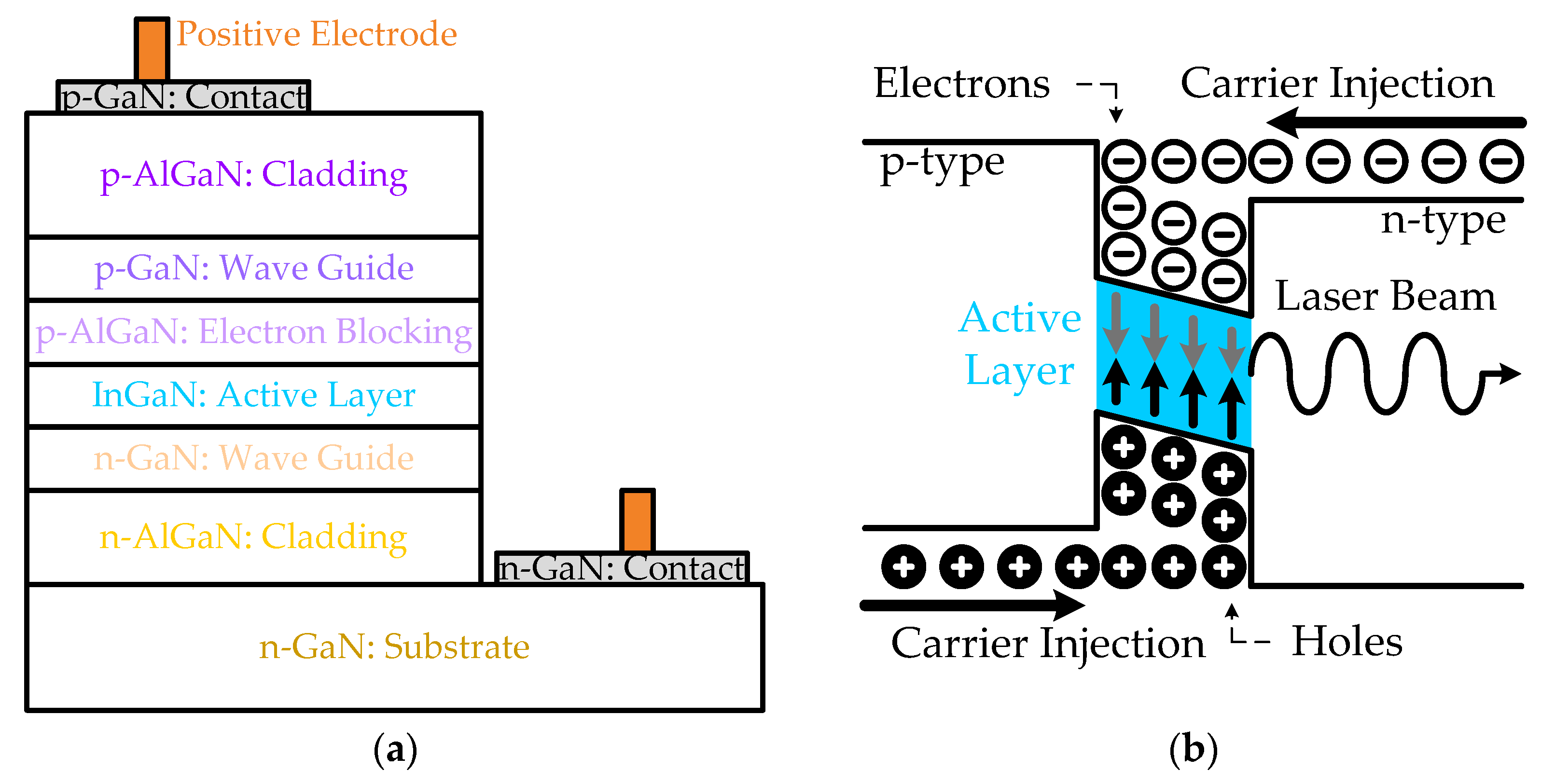
1. Introduction
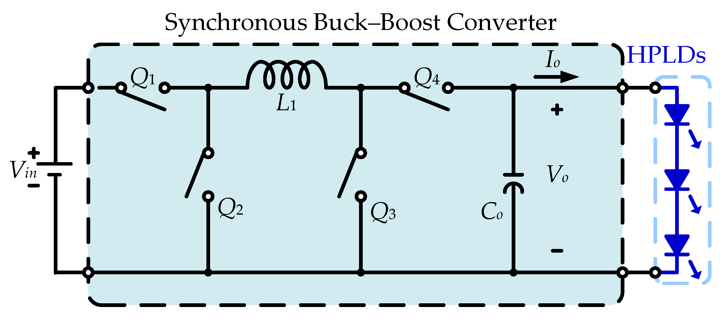
2. Power Converter Principle
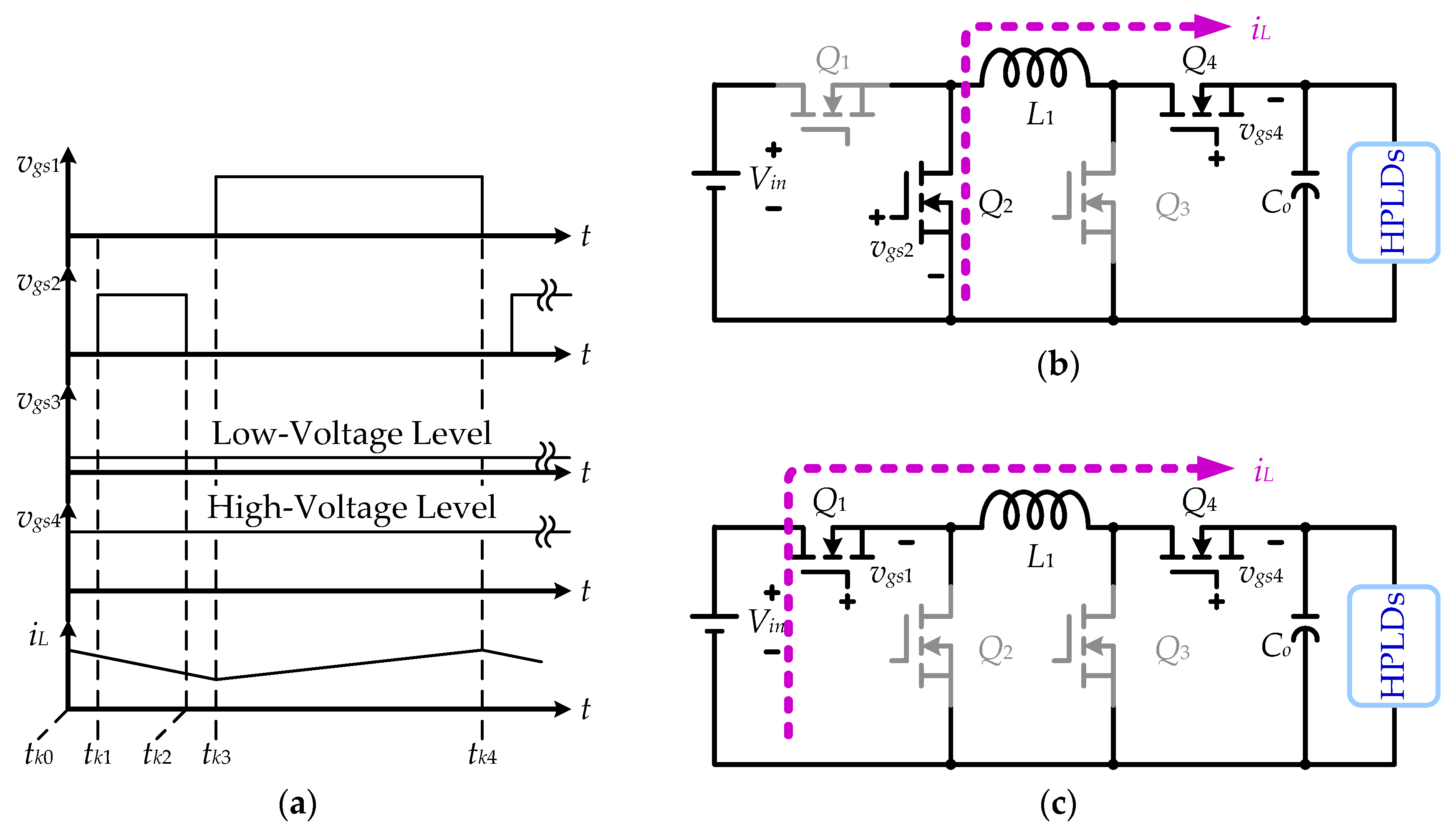
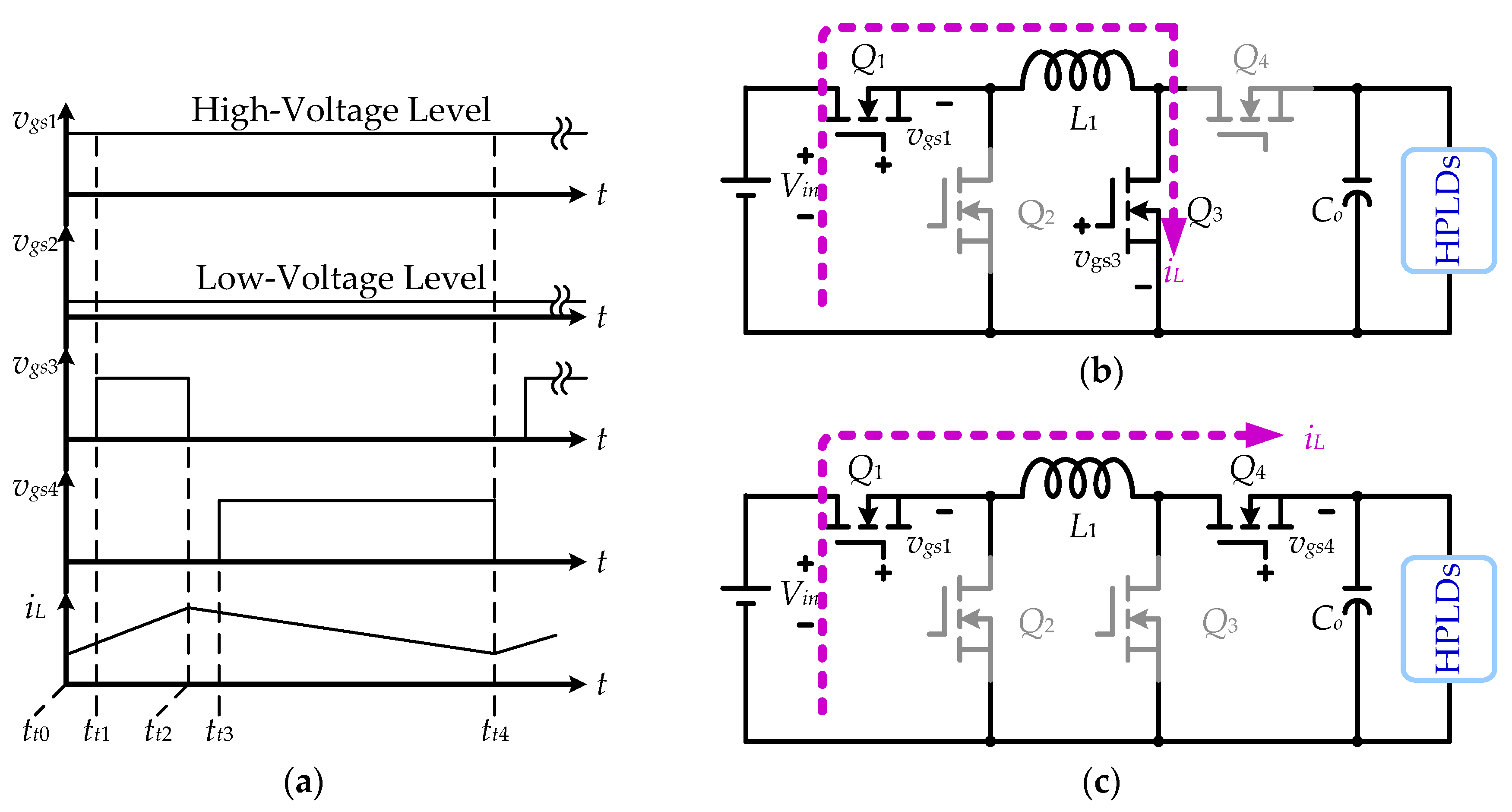
2.1. Buck Mode Principle
2.2. Boost Mode Principle
2.3. Designs of Output Capacitor and Inductor
2.3.1. SBBC Inductor for Buck Mode
2.3.2. SBBC Inductor for Boost Mode
2.3.3. SBBC Output Capacitor
- SBBC Output Capacitor for Buck Mode
- SBBC Output Capacitor for Boost Mode
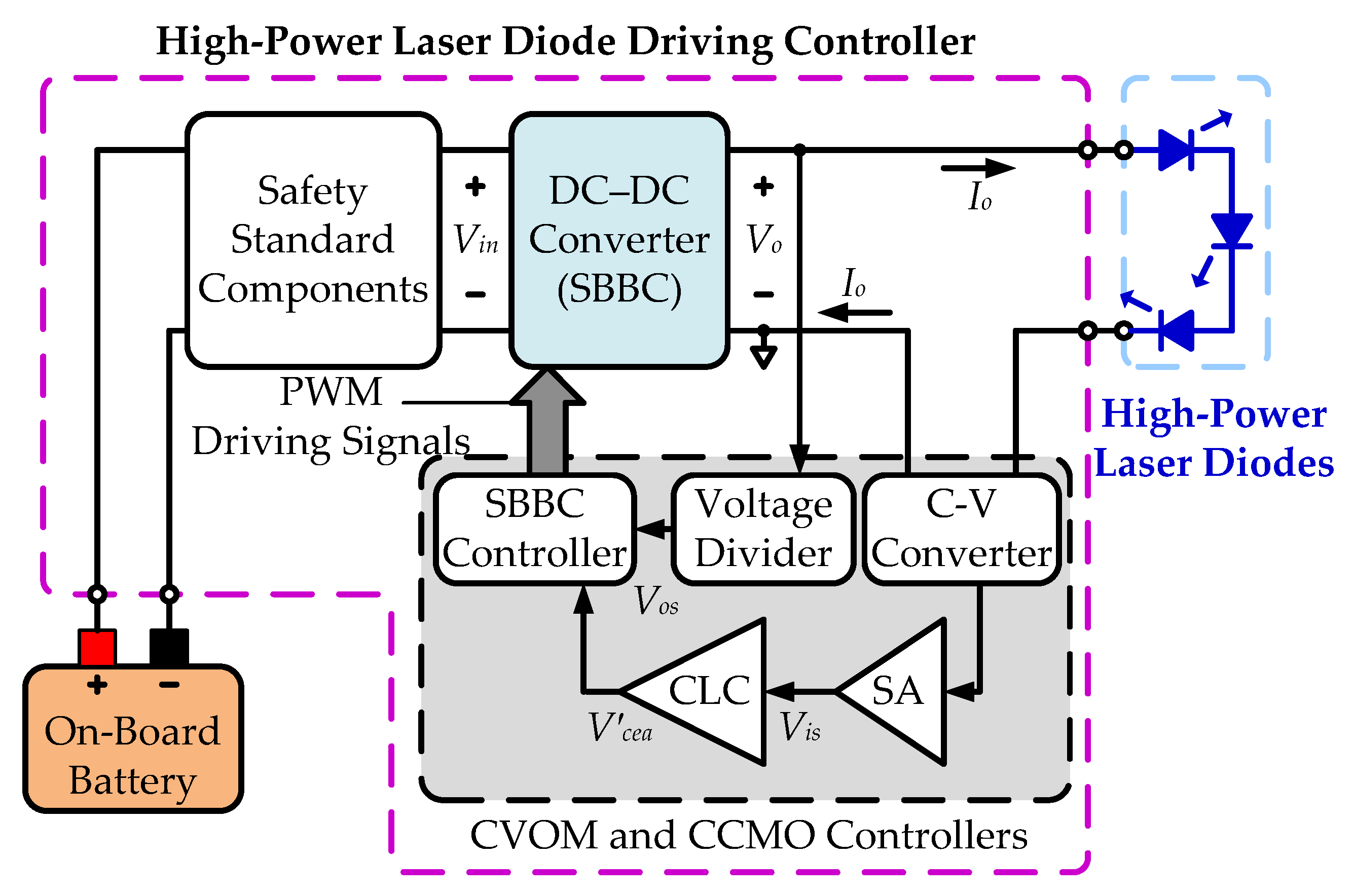
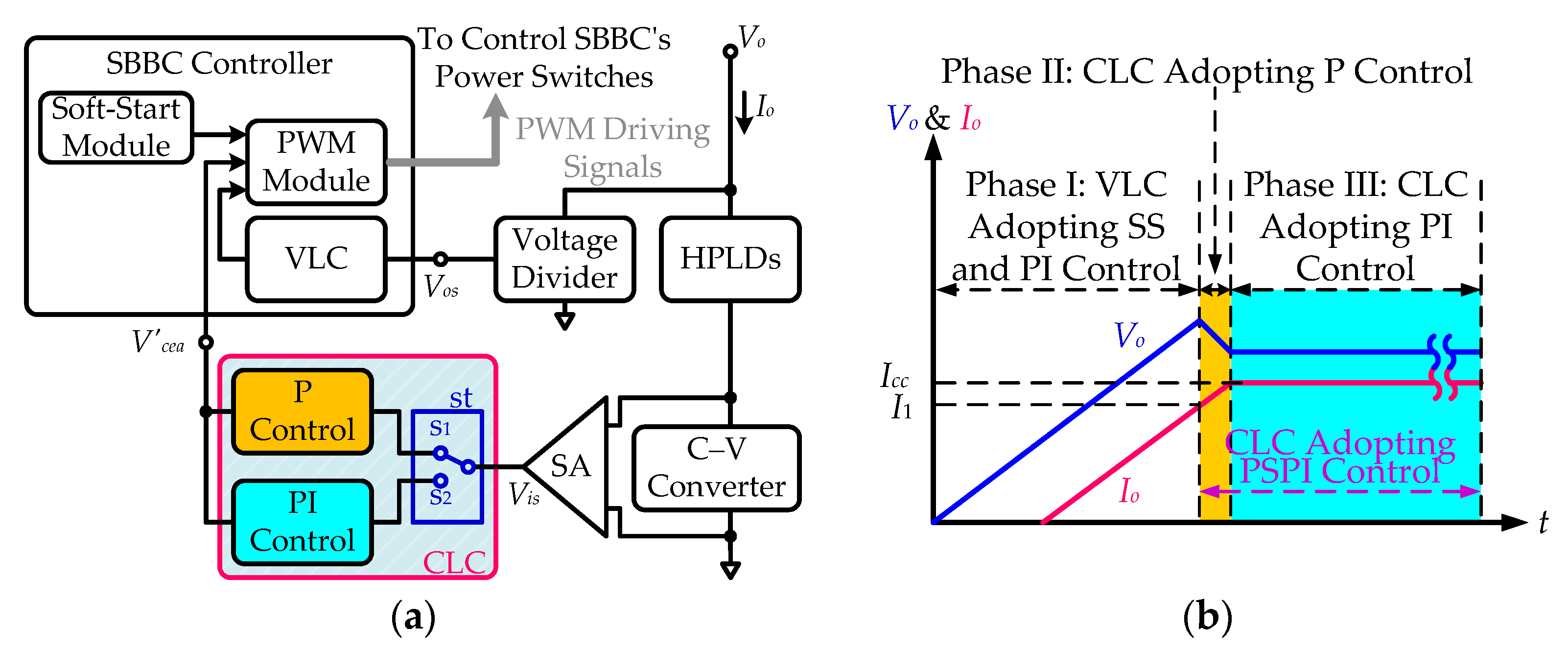
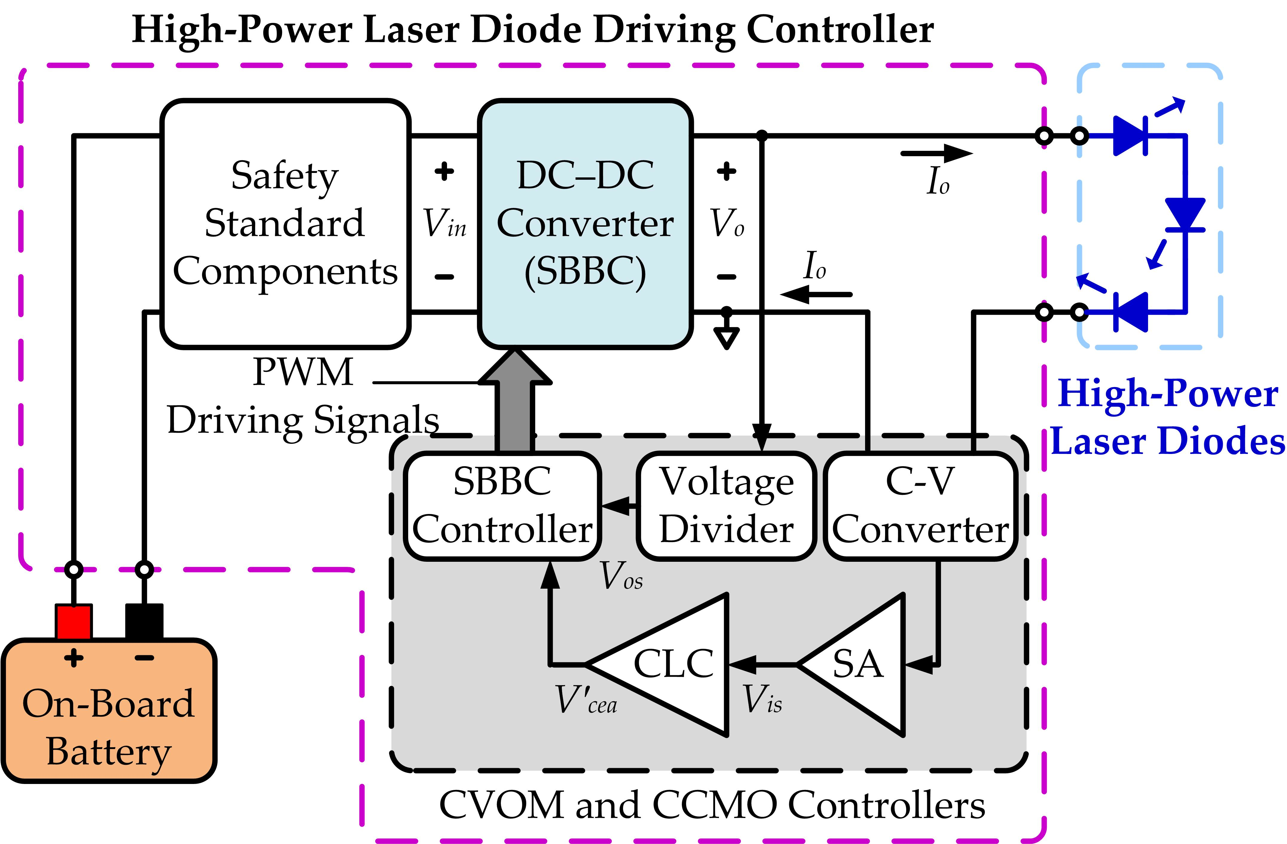
3. HPLDDC Control Loop
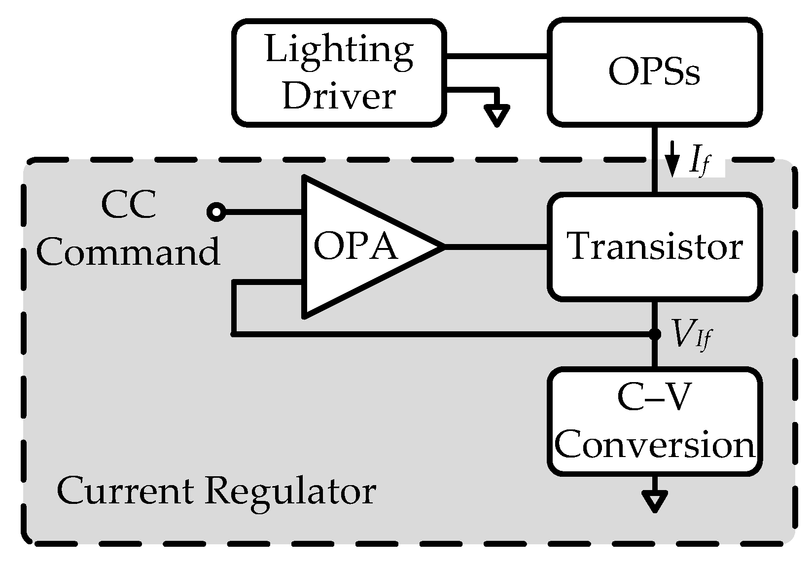
3.1. Constant-Current Sink Control
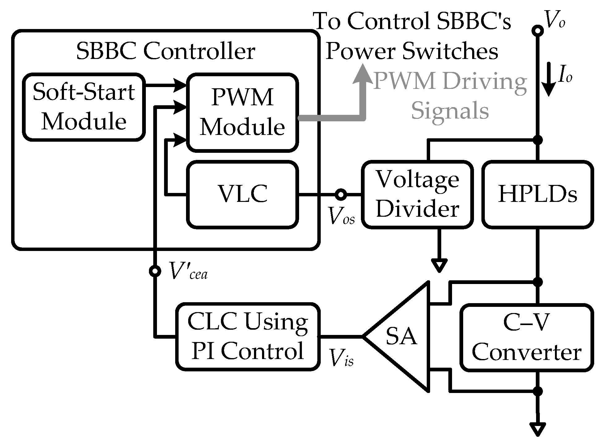
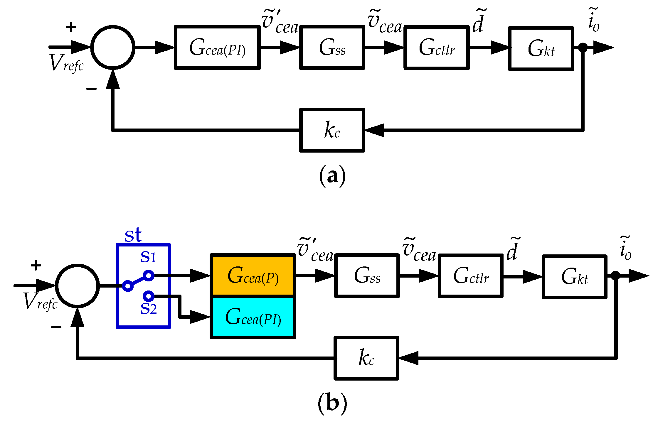
3.2. Constant-Current Source Driving and CLC Using PI Control
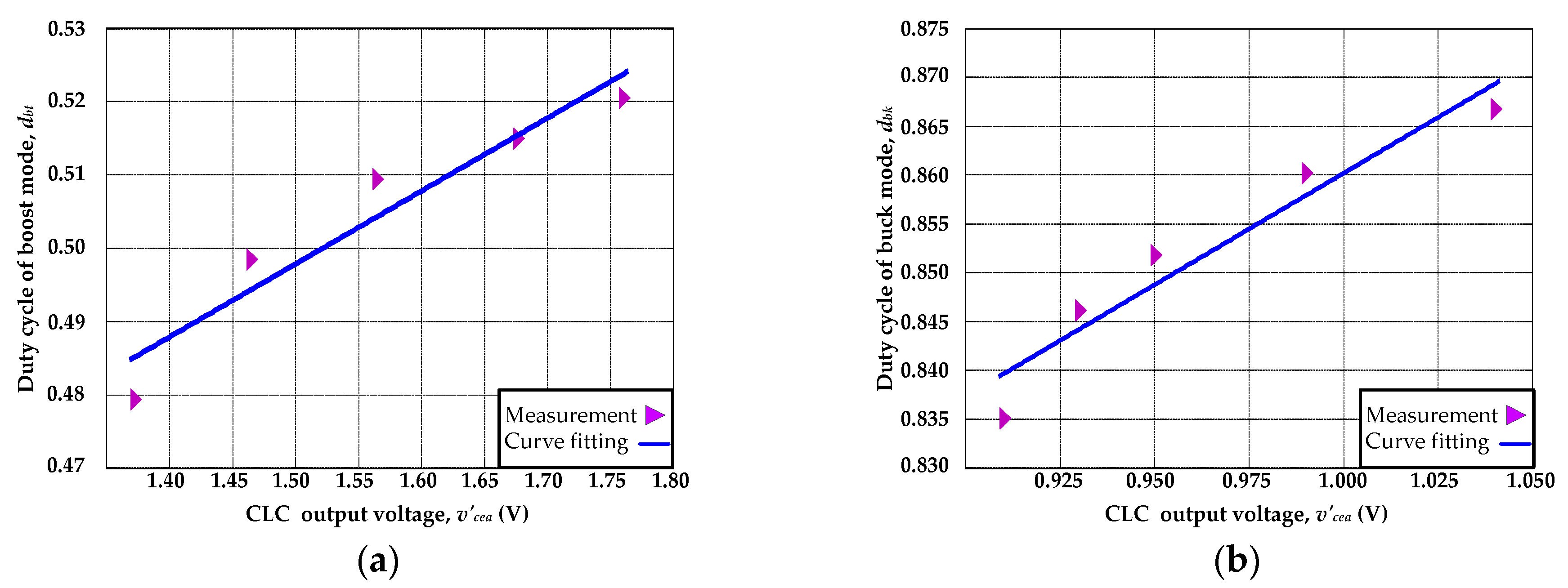
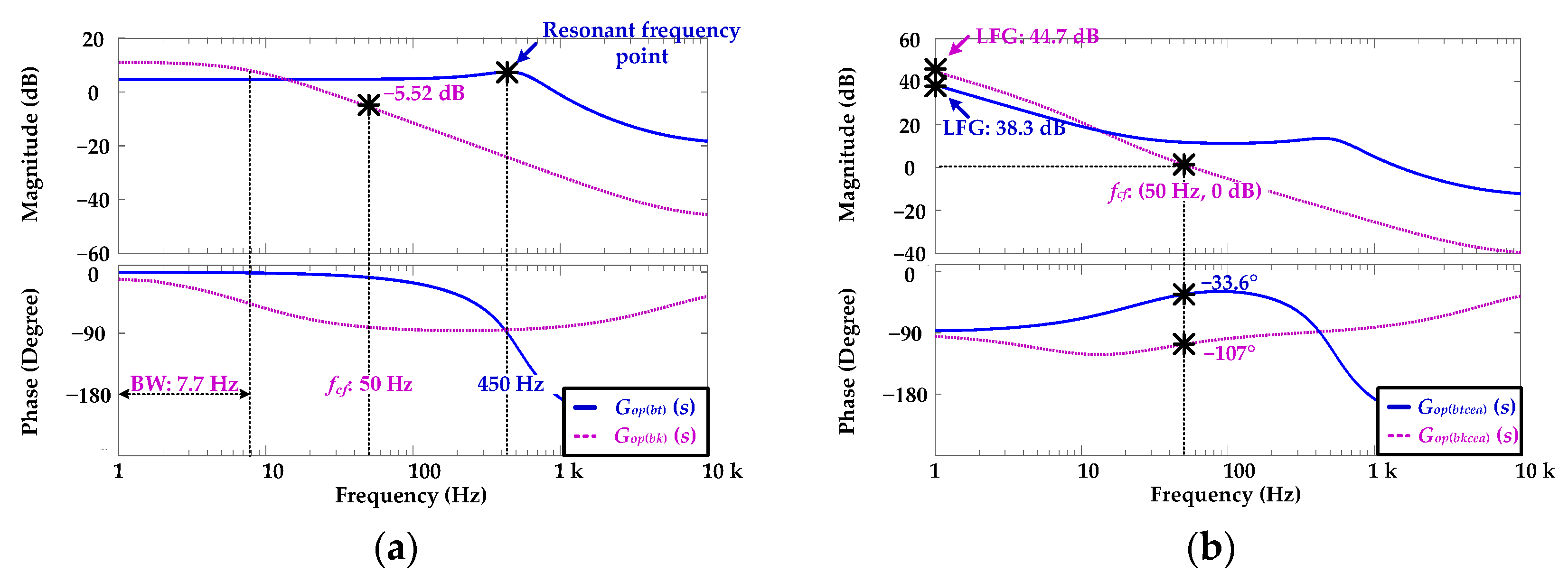
3.3. Constant-Current Source Driving and CLC Using PIAP Control
4. Design Consideration and Simulation
4.1. Inductor Value Calculation
4.2. Output Capacitor Value Calculation
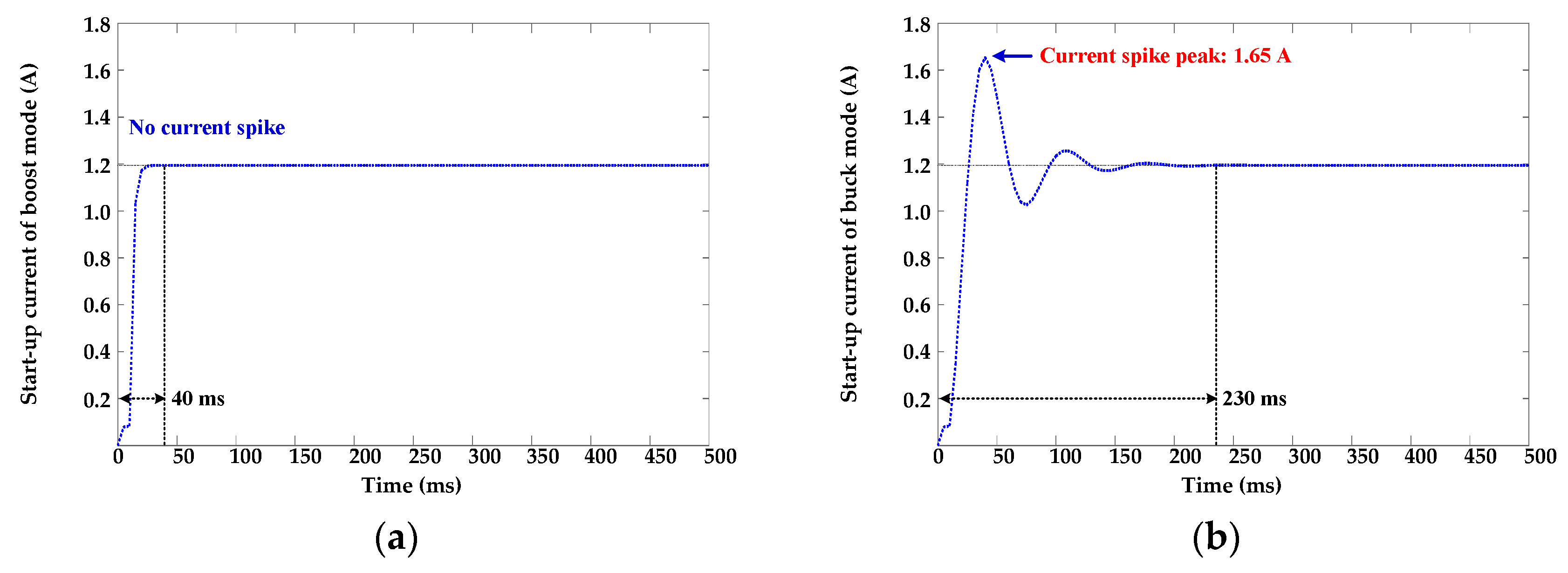
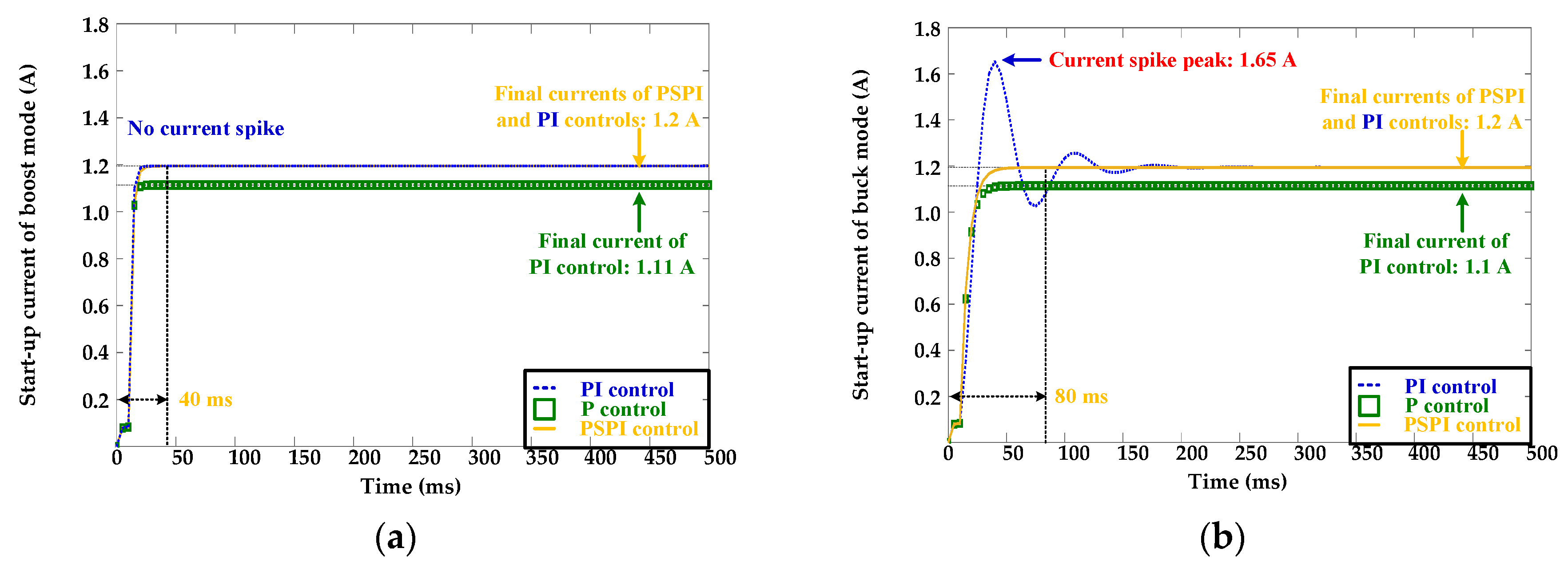
4.3. HPLDDC Current Loop Analysis and Simulation
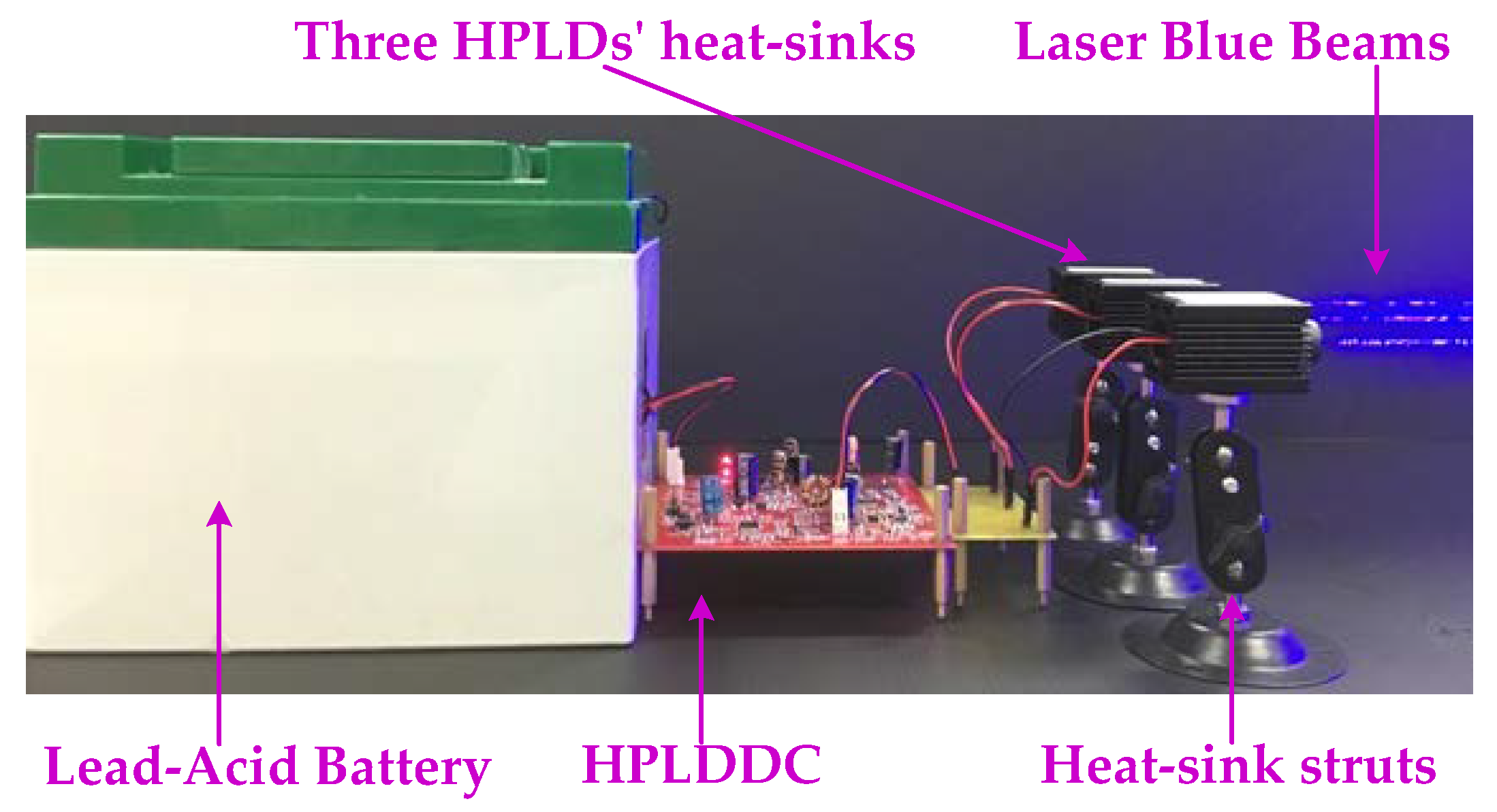
5. Experimental Results
5.1. CLC Using PI Control Method
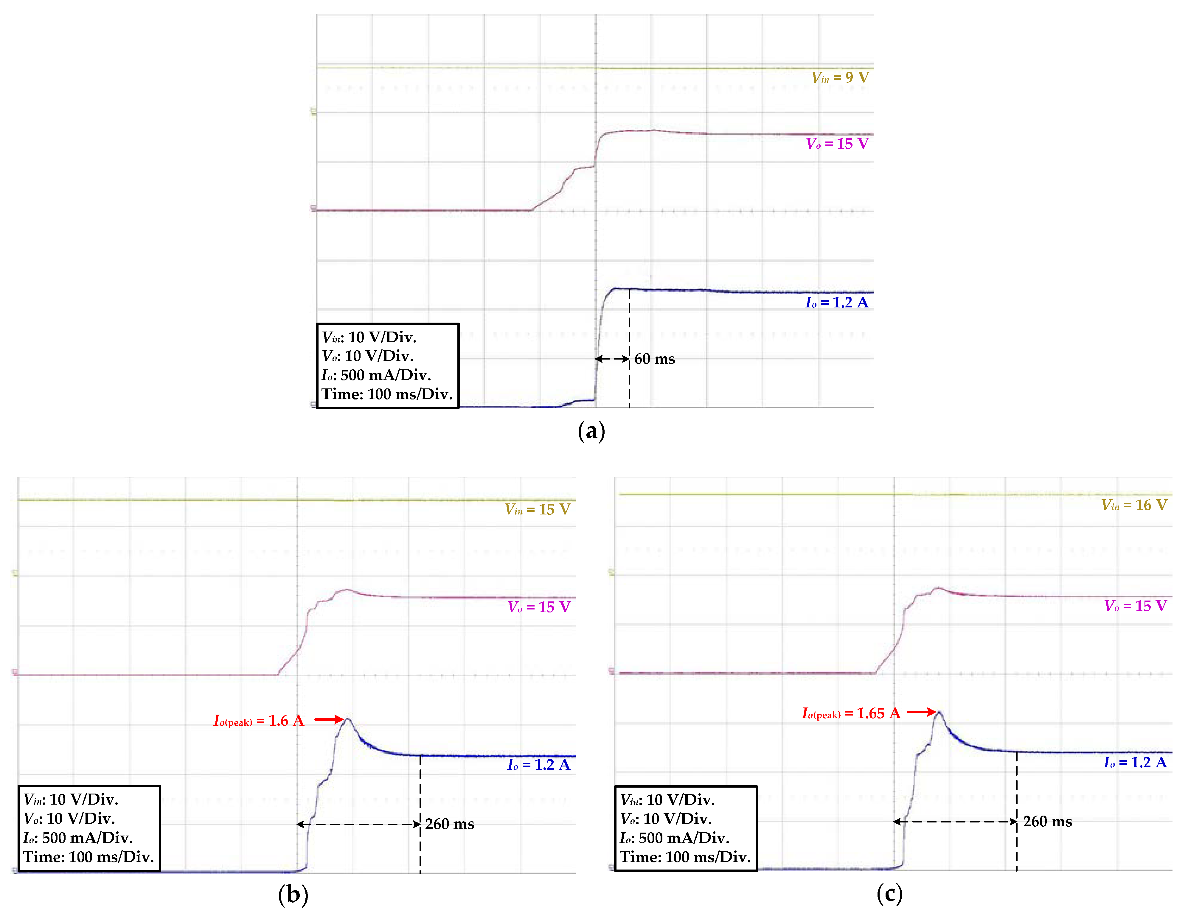
- At a Vin of 9 V, the HPLDDC operated in the boost mode because (Vin = 9 V) < (Vo = 15 V), and a slight current spike was observed, with a peak value of 1.4 A, and the settling time was 60 ms (simulation was 40 ms), as shown in Figure 15a.
- At a Vin of 16 V, the HPPLD operated in the buck mode because (Vin = 16 V) > (Vo = 15 V), and the current spike was observed, with a peak was 1.65 A. This peak value was also over the HPLD maximum operating current of 1.5 A. Then, the settling time was 260 ms (simulation was 230 ms), as shown in Figure 15c.
5.2. CLC Using PIAP Control Method
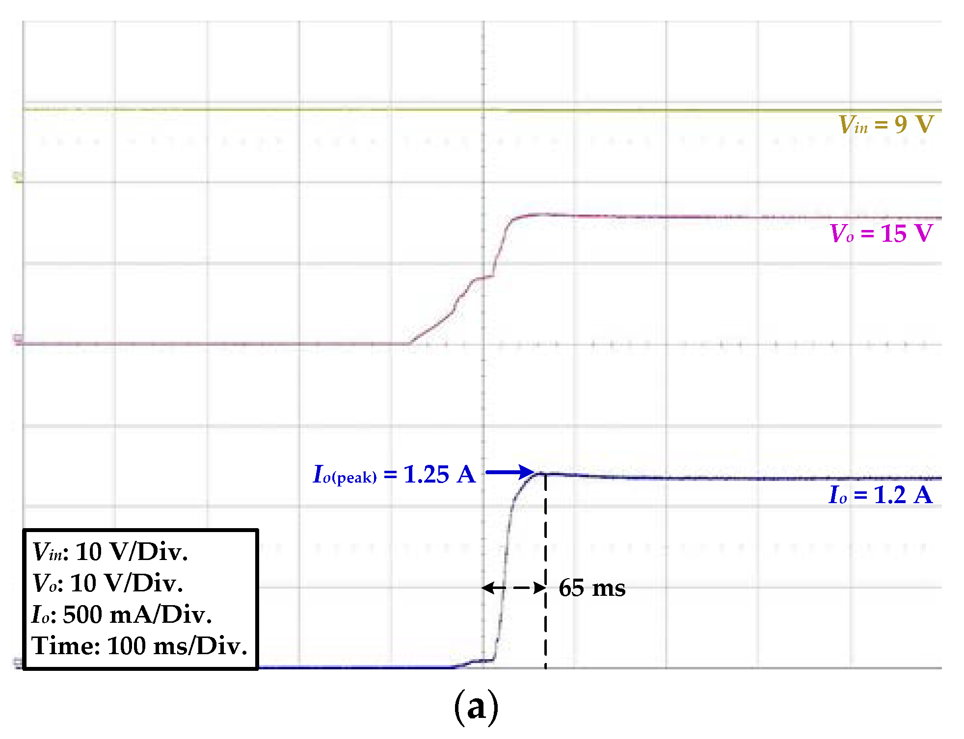
- At a Vin of 9 V, the HPPLD operated the in the boost mode, and a slight current spike with a peak value of 1.25 A was observed. The settling time was 65 ms (simulation was 40 ms), as shown in Figure 16a.
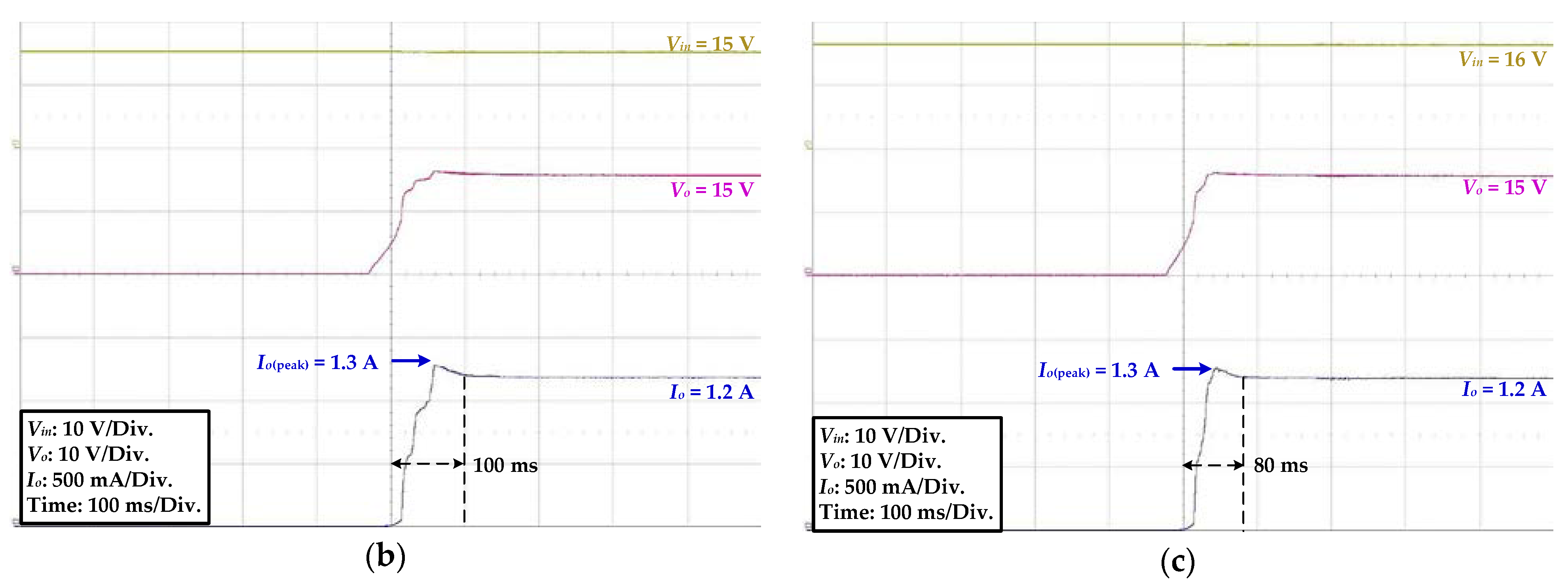
- At a Vin of 15 V, the HPPLD operated in the buck–boost mode, a slight current spike was observed, with a peak of 1.3 A, which was lower than the HPLD maximum operating current of 1.5 A. The settling time was 100 ms, as shown in Figure 16b.
- At a Vin of 16 V, the HPPLD operated in the buck mode, and a slight current spike with a peak of 1.3 A was observed. This peak value was also lower than 1.5 A. The settling time was 80 ms (simulation was 80 ms), as shown in Figure 16c.
6. Conclusions
Author Contributions
Funding
Acknowledgments
Conflicts of Interest
References
- Abu-Ageel, N.; Aslam, D. Laser-driven visible solid-state light source for etendue-limited applications. IEEE/OSA J. Disp. Technol. 2014, 10, 700–703. [Google Scholar] [CrossRef]
- Longa, X.; Heb, J.; Zhouc, J.; Fangc, L.; Zhoub, X.; Renb, F.; Xu, T. A review on light-emitting diode based automotive headlamps. Renew. Sustain. Energy Rev. 2015, 41, 29–41. [Google Scholar] [CrossRef]
- Ji, E.K.; Song, Y.H.; Lee, M.J.; Yoon, D.H. Thermally stable phosphor-in-glass for enhancement of characteristic in high power LED applications. Mater. Lett. 2015, 157, 89–92. [Google Scholar] [CrossRef]
- Wu, H.; Zhang, X.; Ge, P. Modular design of a high-efficiency LED headlamp system based on freeform reflectors. Opt. Laser Technol. 2015, 72, 79–85. [Google Scholar] [CrossRef]
- Aoike, N.; Hoshino, M.; Iwabuchi, A. Automotive HID headlamps producing compact electronic ballasts using power ICs. IEEE Ind. Appl. Mag. 2002, 8, 37–41. [Google Scholar] [CrossRef]
- Chang, Y.N.; Cheng, H.L.; Chang, C.H.; Yen, H.C.; Lin, R.Z. An AC/DC LED driver with unity power factor and soft switching. Appl. Sci. 2018, 8, 780. [Google Scholar] [CrossRef]
- Cheng, C.A.; Chang, E.C.; Tseng, C.H.; Chung, T.Y. A single-stage LED tube lamp driver with power-factor corrections and soft switching for energy-saving indoor lighting applications. Appl. Sci. 2017, 7, 115. [Google Scholar] [CrossRef]
- Cheng, H.L.; Moo, C.S.; Yang, C.S.; Huang, C.K. Analysis and implementation of an HPF electronic ballast for HID lamps with LFSW voltage. IEEE Trans. Power Electron. 2012, 27, 4584–4593. [Google Scholar] [CrossRef]
- Chiu, H.J.; Lo, Y.K.; Yao, C.J.; Cheng, S.J. Design and implementation of a photovoltaic high-intensity-discharge street lighting system. IEEE Trans. Power Electron. 2011, 26, 3464–3471. [Google Scholar] [CrossRef]
- Keyence Corp. Laser Technical Guide; Keyence Corp.: Osaka, Japan, 2015. [Google Scholar]
- USHIO Opto Semiconductors Inc. Chip Structure and Lasing Modes; USHIO Opto Semiconductors Inc.: Kyoto, Japan, 2014. [Google Scholar]
- OSRAM Opto Semiconductors Inc. Using OSRAM OS Visible InGaN Laser Diodes; OSRAM Opto Semiconductors Inc.: Regensburg, Germany, 2013. [Google Scholar]
- Seok, J.K.; Kim, K.T.; Lee, D.C. Automatic mode switching of P/PI speed control for industry servo drives using online spectrum analysis of torque command. IEEE Trans. Ind. Electron. 2007, 54, 2642–2647. [Google Scholar] [CrossRef]
- Roberto, M.C.; Edmundo, B.H.; Marco, A.; Caporal, M. DSP-based digital torque/motion control of DC motors for direct-drive industrial robotic applications. In Proceedings of the 2010 IEEE Electronics, Robotics and Automotive Mechanics Conference, Morelos, Mexico, 28 September–1 October 2010; pp. 613–618. [Google Scholar]
- Naouar, M.W.; Naassani, A.; Monmasson, E.; Slama-Belkhodja, I. FPGA-based speed control of synchronous machine using a P-PI controller. In Proceedings of the 2006 IEEE International Symposium on Industrial Electronics, Montreal, Canada, 9–13 July 2006; pp. 1527–1532. [Google Scholar]
- Robert, E.W.; Maksimovic, D. Fundamental of Power Electronics, 2nd ed.; Kluwer Academic Publishers: Norwell, MA, USA, 2001; ISBN 0792372700. [Google Scholar]
- Texas Instruments Inc. LM5118-Q1 Wide Voltage Range Buck-Boost Controller; Texas Instruments Inc.: Dallas, TX, USA, 2004. [Google Scholar]
- Wu, C.Y.; Wu, T.F.; Tsai, J.R.; Chen, Y.M.; Chen, C.C. Multistring LED backlight driving system for LCD panels with color sequential display and area control. IEEE Trans. Ind. Electron. 2008, 55, 3791–3799. [Google Scholar]
- Chiu, H.J.; Cheng, S.J. LED backlight driving system for large-scale LCD panels. IEEE Trans. Ind. Electron. 2007, 54, 2751–2760. [Google Scholar] [CrossRef]
- Rogers, E. Understanding Buck Power Stages in Switch Mode Power Supplies: Application Report; Texas Instruments Inc.: Dallas, TX, USA, 1999. [Google Scholar]
- Fronczak, K. Stability Analysis of Switched Dc-Dc Boost Converters for Integrated Circuits. Master's Thesis, Rochester Institute of Technology, Rochester, NY, USA, 1 August 2013. [Google Scholar]
- Vorperian, V. Simplified analysis of PWM converters using model of PWM switch part I: Continuous conduction mode. IEEE Trans. Aerosp. Electron. Syst. 1990, 26, 490–496. [Google Scholar] [CrossRef]
- Vorperian, V. Simplified analysis of PWM converters using model of PWM switch. II. Discontinuous conduction mode. IEEE Trans. Aerosp. Electron. Syst. 1990, 26, 497–505. [Google Scholar] [CrossRef]
- Zhang, H.J. Modeling and Loop Compensation Design of Switching Mode Power Supplies; Linear Tech. Corp.: Milpitas, CA, USA, 2015. [Google Scholar]

| CC Control Technology | Driver Output Mode | Driving Current Compensation | Start-up Current Spike Mitigation |
|---|---|---|---|
| CC Sink | CVOM | N/A | N/A |
| CC Source Using Proportional-Integral (PI) Control | CVOM & CCOM | PI compensation | N/A |
| CC Source Using Proportional-Integral Associating Proportional (PIAP) Control | CVOM & CCOM | P and PI compensations | Effectual |
| Notation | Transfer Function (TF) Parameter for Buck Mode | TF Parameter for Boost Mode |
|---|---|---|
| nu2 | 0 | −L1rc/rhpld |
| nu1 | rcCo | rc(1 − Dbt)2 − L1/(rhpldCo) – rcrL/rhpld |
| nu0 | 1 | −rL/(rhpldCo) + (1 − Dbt)2/Co |
| de2 | (L1Co)(rhpld + rc)/(rhpld + rL) | L1(rc/rhpld + 1) |
| de1 | Corc + rhpldrL/(rhpld + rL) + L1/(rhpld + rL) | rc(1 − Dbt)2 + rL + rcrL/rhpld + L1/(rhpldCo) |
| de0 | 1 | rL/(rhpldCo) + (1 − Dbt)2/Co |
| kcon | Vin(max)/[rhpld (rhpld + rL)] | Vo/[rhpld (1 − Dbt)] |
| Depiction | Specification |
|---|---|
| Operating forward voltage (VLD1) at the operating forward current ILD1 = 0.9 A | 4.7 V |
| Operating forward voltage (VLD2) at the operating forward current ILD2 = 1.2 A | 4.8 V |
| Optical output power | 1.6 W |
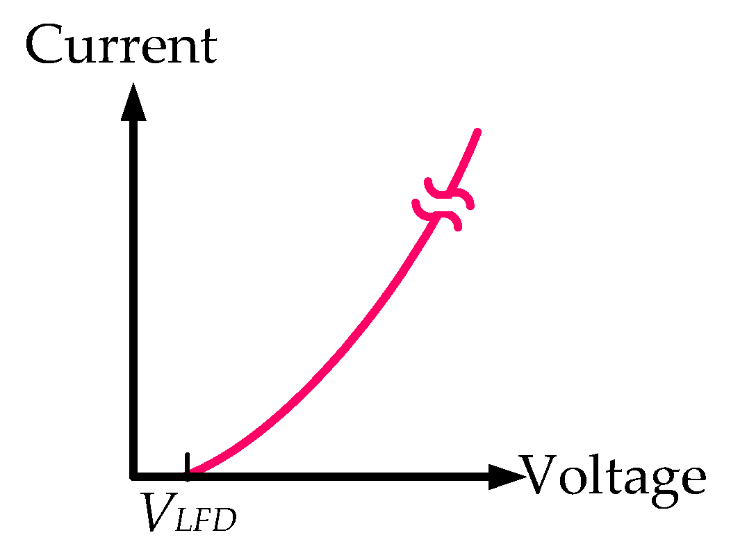
| Maximum operating current | 1.5 A |
| Laser emission wavelength | 450 nm |
| Operating temperature range | −40 °C to 85 °C |
| Package | TO56 |
| Parameter | Specification | Parameter | Specification |
|---|---|---|---|
| Vin(min) | 9 V | Vin(max) | 16 V |
| Vo(min) | 13 V | Vo(max) | 16 V |
| Io | 1.2 A | fs | 400 kHz |
| α | 1% | β | 20% |
| Notation | Calculating Value | Notation | Calculating Value |
|---|---|---|---|
| Lbk | 9.1 μH | Lbt | 20.5 μH |
| Cobk | 9.4 μF | Cobt | 4.1 μF |
| ESRbk | 109 mΩ | ESRbt | 62 mΩ |
| Circuit Element | Type-Number | Specification |
|---|---|---|
| Q1, Q2, Q3, Q4 | IRF7478PBF | Maximum drain–source voltage is 60 V Drain–source turning on resistance is 26 mΩ Drain current is 7 A at 25 °C |
| L1 | CS127060 | Inductance value: 30 μH Material: Sendust |
| Co | EEU-FR1E471Y | Inductance value: 470 μF ESR ≤ 41 mΩ, Aluminum electrolytic capacitance |
| Blue-beam HPLDs | PL TB405B | Semiconductor laser diode Material: InGaN-base Laser emission: Blue beam. See the Table 3 |
| Operational amplifier of SA and CLC | LM258ADR | Range of DC power supply: 3 V to 32 VOpen-loop differential voltage gain: 100 dB Unity gain bandwidth: 0.7 MHz Operational amplifier, package: SO8 Operating temperature: −40 °C to 85 °C. |
| Parameter | Value | Parameter | Value |
|---|---|---|---|
| rc | 41 mΩ | rL | 68 mΩ |
| Vin(max) | 16 V | Co | 470 μF |
| L1 | 30 μH | rhpld | 0.99 Ω |
| Dbt | 0.437 |
© 2018 by the authors. Licensee MDPI, Basel, Switzerland. This article is an open access article distributed under the terms and conditions of the Creative Commons Attribution (CC BY) license (http://creativecommons.org/licenses/by/4.0/).
Share and Cite
Pai, K.-J.; Qin, L.-D.; Lin, C.-H.; Tang, S.-Y. Start-Up Current Spike Mitigation of High-Power Laser Diode Driving Controller for Vehicle Headlamp Applications. Appl. Sci. 2018, 8, 1532. https://doi.org/10.3390/app8091532
Pai K-J, Qin L-D, Lin C-H, Tang S-Y. Start-Up Current Spike Mitigation of High-Power Laser Diode Driving Controller for Vehicle Headlamp Applications. Applied Sciences. 2018; 8(9):1532. https://doi.org/10.3390/app8091532
Chicago/Turabian StylePai, Kai-Jun, Lin-De Qin, Chang-Hua Lin, and Sheng-Yi Tang. 2018. "Start-Up Current Spike Mitigation of High-Power Laser Diode Driving Controller for Vehicle Headlamp Applications" Applied Sciences 8, no. 9: 1532. https://doi.org/10.3390/app8091532
APA StylePai, K.-J., Qin, L.-D., Lin, C.-H., & Tang, S.-Y. (2018). Start-Up Current Spike Mitigation of High-Power Laser Diode Driving Controller for Vehicle Headlamp Applications. Applied Sciences, 8(9), 1532. https://doi.org/10.3390/app8091532