Article

Effective Modal Volume in Nanoscale Photonic and Plasmonic Near-Infrared Resonant Cavities

1
Department of Electrical Engineering, University of Texas at Dallas, Richardson, TX 75080, USA
2
Department of Electrical and Computer Engineering, University of California San Diego, La Jolla, CA 92093; USA
3
Department of Mechanical Engineering, University of California Berkeley, Berkeley, CA 94720, USA
*
Author to whom correspondence should be addressed.
These authors contributed equally to this work.
Appl. Sci. 2018, 8(9), 1464; https://doi.org/10.3390/app8091464
Submission received: 29 July 2018 / Revised: 17 August 2018 / Accepted: 21 August 2018 / Published: 25 August 2018
(This article belongs to the Section Optics and Lasers)

Abstract

:

Featured Application

A practical guideline to the calculation of effective modal volume for photonic and plasmonic cavities.

Abstract

We survey expressions of the effective modal volume, Veff, commonly used in the literature for nanoscale photonic and plasmonic cavities. We apply different expressions of Veff to several canonical cavities designed for nanoscale near-infrared light sources, including metallo-dielectric and coaxial geometries. We develop a metric for quantifying the robustness of different Veff expressions to the different cavities and materials studied. We conclude that no single expression for Veff is universally applicable. Several expressions yield nearly identical results for cavities with well-confined photonic-type modes. For cavities with poor confinement and a low quality factor, however, expressions using the proper normalization method need to be implemented to adequately describe the diverging behavior of their effective modal volume. The results serve as a practical guideline for mode analysis of nanoscale optical cavities, which show promise for future sensing, communication, and computing platforms.

1. Introduction

Semiconductor nanolasers serve simultaneously as a platform for studying intriguing fundamental physics and as a technologically relevant solution for next generation photonic integrated circuits [1,2]. A major drive in the study and application of nanoscale cavities rests in the Purcell effect, which describes the inverse relation between cavity mode volume and the rate of spontaneous emission [3,4]. Smaller cavities generally permit higher rates of spontaneous emission and a greater ratio of spontaneous emission channeled into the lasing mode, which, in principle, provides increased modulation bandwidths and lower lasing thresholds [5,6]. In many nanoscale structures, however, the physical volume of the cavity does not reflect the volume of the cavity mode. Therefore, the effective modal volume, Veff—a unitless quantity normalized with respect to (λ0/na)3, was introduced to account for this discrepancy [7]. A complementary expression, the confinement factor, Г, may be defined to express the ratio of the volume of the active region, Va, to Veff, namely [8].
Γ V a   V e f f
In purely dielectric cavities with a large physical volume with respect to the cubic wavelength, Г ≈ 1 because the mode is completely confined to the active region. As the active region volume approaches the diffraction limit (approximately given by (λ0/(2na))3, where λ0 and na are the vacuum wavelength and the real part of the active region refractive index, respectively), the cavity mode becomes less confined and Г < 1. Eventually, when Va/(λ0/(2na))3 << 1, modes are no longer supported in the purely dielectric cavity of which the physical size is below the diffraction limit in all three dimensions. To continue reducing cavity volume, the incorporation of metals becomes inevitable [9]. The plasmonic modes supported by metal–dielectric interfaces in such cavities exhibit considerably different modal profiles from their dielectric counterparts. Namely a substantial portion of modal energy rests at the metal-dielectric interface rather than in the center of a purely dielectric region.
Calculation of Veff in three-dimensional (3D) cavities generally requires use of numerical methods due to the geometric and material complexity of the cavities. Physically, the cavity mode is a spatial distribution of electromagnetic energy [10]. Therefore, the calculation essentially requires a comparison of integration of the electromagnetic energy density over the active region domain, Ua, to the integration of the energy density over the entire simulation domain, U. If the simulation domain consists only of dielectric materials, then this calculation is straightforward, and can be expressed as:
Γ = Ξ e , a   + Ξ m , a Ξ e + Ξ m = V a d 3 r a U e ( r ) + V a d 3 r a U m ( r ) V d 3 r U e ( r ) + V d 3 r U m ( r )
where Ξ is the energy, r is the position vector, and the e, m, and a subscripts refer to electrical energy, magnetic energy, and active region respectively. For a simulation of non-absorbing and non-dispersive materials, the stored electrical and magnetic energy are identical [11]. Hence, Equation (2) may be simplified to its more commonly seen form of:
Γ = Ξ e , a   Ξ e = V a d 3 r a U e ( r ) V d 3 r U e ( r ) = V a d 3 r a ( D ( r ) · E ( r ) * ) V d 3 r ( D ( r ) · E ( r ) * ) = V a d 3 r a ( ε 0 ε r ( r ) | E ( r ) | 2 ) V d 3 r ( ε 0 ε r ( r ) | E ( r ) | 2 ) = V a d 3 r a ( ε 0 ε r ( r ) | E ( r ) | 2 ) α V α d 3 r α ( ε 0 ε r , α ( r α ) | E α ( r α ) | 2 )
where D and E are the displacement and electric field vectors, respectively (* denotes the conjugated form of the electric field, therefore, the inner product would be the norm of the electric field), ε0 is the permittivity in vacuum, and εr = εR + iεI is the, generally, complex valued relative permittivity, with the R and I subscripts denoting the real and imaginary part, respectively. In the last equality, α represents each unique material domain in the simulation over which volume integration must be executed, with the total energy being the sum over these domains. For the study presented in the proceeding sections, we will consider only non-magnetic materials and therefore use Equation (3) as our reference point.
For sake of clarity, we define a material as dielectric or metallic at a given wavelength when εR > 0 and εR < 0, respectively. Hence, the same “material” can behave as both dielectric and metal if the simulation includes dispersion over the range of wavelengths in which εR changes sign. Also, we define a material as absorptive at a given wavelength when εI < 0 (the negative sign is used to be in accordance with the expression in our simulation software, COMSOL Multiphysics® 5.3 (Burlington, MA, USA)). As most dielectric materials show very weak dispersion and absorption property in the optical regime, if all materials are dielectric, the evaluation of Equation (3) is straightforward, as all of the terms are positive. If some materials are metallic, but the mode is confined primarily to a dielectric region, Equation (3) remains useful because the denominator remains positive and the small amount of energy contribution from the metallic region introduces only negligible errors in the calculation. However, for cavities supporting surface plasmon polariton (SPP) modes or localized surface plasmon resonance (LSPR) modes where the electric field is strongly confined at the metal–dielectric interface, the amount of energy stored and dissipated by metal is no longer negligible. Equation (3) becomes invalid because the resulting negative energy has no physical meaning.
To circumvent this problem, the real part of the permittivity in Equation (3) can be replaced by an average permittivity, defined as [12]. As ω γ (damping constant) in most of the optical applications, both ε g and ( ε g ( ω ) + ε R ( ω ) ) / 2 are positive.
ε avg   ( r , ω ) = ( ε g ( r , ω ) + ε R ( r , ω ) ) 2
where ω is the angular frequency, related to the vacuum wavelength via the vacuum speed of light, c, by ω = 2πc/λ0, and εg is the group permittivity. The latter is calculated as:
ε g = [ ω ε R ( r , ω )   ] ω
Use of Equation (4) in place of simply εr accounts for the physical effects of dispersion and usually ensures mathematically that the all the terms in the denominator of Equation (3) will be positive because in most cases εg + εR > 0. For example, use of the Drude model for the complex permittivity of gold (Au) leads to εg + εR > 0 [12]. However, use of experimental data [13] for the permittivity of Ag may lead to εg + εR < 0, such that εavg < 0. In this case, use of εr in Equation (3) may be replaced directly by Equation (5), which will always be positive [14,15,16].
Despite the circumvention of the failure of Equation (3) via Equations (4) and (5), a number of different expressions for the effective modal volume have appeared in the literature [17,18,19,20,21]. It is the purpose of this paper to assess the utility of these expressions for the design and analysis of nanoscale photonic and plasmonic cavities. For concreteness, we evaluate the expressions for near-infrared (IR) resonant cavities. In Table 1, we list all three different nanoscale cavities we have evaluated, and categorize them according to the optical mode they support. Therefore, we provide a practical guideline on how to implement each effective modal expression. It should be understood, however, that our approach could be applied to cavities supporting modes at other frequencies as well.
The paper is organized as follows. In Section 2 we expand upon the introduction and review the various expressions for Veff found in the literature. Next, in Section 3 we apply these expressions to several canonical cavity geometries, including a metallo-dielectric cavity that supports photonic modes [22] and a coaxial cavity that supports plasmonic modes [6]. In all cases, indium gallium arsenide phosphide (InGaAsP) serves as the active region material, with alloy composition chosen such that emission occurs in the wavelength range of 1260 nm < λ0 < 1590 nm. For the coaxial geometry, we study both Ag and aluminum-doped zinc oxide (AZO) as the cladding materials, whereas only Ag is used for the metallo–dielectric geometry. The plasma frequency of Ag and AZO lie in the ultraviolet and near-IR wavelengths, respectively, with the latter being tunable depending on its alloy composition [23]. Therefore, we compare cases when the active material emission frequency and the cavity resonance frequency are far from and close to the plasma frequency of the constituent metal. Room temperature conditions are assumed for all calculations and values of permittivity are taken from the literature [23,24,25]. It should be emphasized that in calculating Veff, we include both the real and imaginary parts of the metal permittivity to account for realistic absorption losses. However, we use only the real part of the InGaAsP permittivity because we are primarily interested in the degree to which electromagnetic energy may be stored in the active region. When considering absorption or amplification of energy in the active region, the numerator of Equation (3) can be used with the substitution of εI for εr, which has been theoretically proved and verified by numerical simulation, respectively [26,27]. In Section 4, we discuss our results and present a metric for comparing the robustness of the various expressions. We conclude the paper in Section 5.

2. Materials and Methods

In this section, we present five expressions for Veff from the literature. The first expression, Veff,1, was presented for use in a photonic crystal cavity with an air gap and containing only dielectric materials [17]. It is:
V e f f , 1   = α V α d 3 r α ( ε α ( r α ) | E α ( r α ) | 2 ) ε ( r max ) max ( | E ( r max ) | ) 2
The denominator of Equation (6) includes the maximum of the electric field, where rmax denotes the position of electric field antinode. Additionally, the permittivity of the denominator equals that of the material in which the maximum electric field antinode is located.
The second expression, Veff,2 was used in the analysis of metallic nanocube antennas [18]. It defines the effective volume as the ratio of total electrical energy to the peak value of electrical energy density. Using the earlier introduced notation:
V e f f , 2   = Ξ e max ( U e ) = α V α d 3 r α ( ε α ( r α ) | E α ( r α ) | 2 ) max ( ε ( r ) | E ( r ) | 2 )
If the peak energy density is located in the active region, then Equation (7) leads to the reference expression for Г, i.e., Equation (3), after division by Va. If the peak electric field lies in the active region, then Equations (6) and (7) yield the same result. However, in some geometries, the peak electric field could reside in a low index region, such as an air gap, while the peak energy density lies in the high index active region, in which case Equations (6) and (7) will yield different results.
The third effective volume expression, Veff,3, was used in the analysis of spontaneous emission enhancement in a dielectric pillar microcavity [19] and a metallo–dielectric cavity [22]. It is:
V e f f , 3   = α V α d 3 r α ( n α ( r α ) 2 | f α ( r α ) | 2 ) n a 2
where f is the normalized electric field such that |f(r)| = 1 at the field antinode. While Equation (8) appears to differ from Equations (6) and (7) in that the electric field is absent from the denominator, the normalization effectively supplies the electric field to both the numerator and denominator. If all materials in the cavity are lossless dielectric and the peak electric field resides in the active region, then Veff,3 yields identical results to Veff,2 and Veff,1. However the use of the active region refractive index in the denominator of Equation (8), regardless of the location of peak field or energy, generally leads to values of Veff,3 different from Veff,1 and Veff,2.
The fourth effective volume expression that we assess, Veff,4, is [20,28,29]:
V e f f , 4   = ( [ 1 V p ] r ) 1
where Vp is defined as:
V p α ( V α d 3 r α σ α ( r α ) E α ( r α ) 2 ) + i ε B ( r ) c 2 ω ˜ c δ V d 2 r E ( r ) 2 ε ( r max ) max ( E ( r max ) ) 2 = ( [ ε ( r max ) max ( E ( r max ) ) 2 α ( V α d 3 r α σ α ( r α ) E α ( r α ) 2 ) + i ε B ( r ) c 2 ω ˜ c δ V d 2 r E ( r ) 2 ] r ) 1 = ( [ ε ( r max ) max ( E ( r max ) ) 2 α ( V α d 3 r α σ α ( r α ) E α ( r α ) 2 ) + i ε B ( r ) c 2 ω ˜ c δ V d 2 r E ( r ) 2 × × α ( V α d 3 r α σ α ( r α ) E α ( r α ) 2 ) i ε B ( r ) c 2 ω ˜ c δ V d 2 r E ( r ) 2 α ( V α d 3 r α σ α ( r α ) E α ( r α ) 2 ) i ε B ( r ) c 2 ω ˜ c δ V d 2 r E ( r ) 2 ] r ) 1 = ( [ ε ( r max ) max ( E ( r max ) ) 2 ( α ( V α d 3 r α σ α ( r α ) E α ( r α ) 2 ) i ε B ( r ) c 2 ω ˜ c δ V d 2 r E ( r ) 2 ) ( α ( V α d 3 r α σ α ( r α ) E α ( r α ) 2 ) ) 2 + ( ε B ( r ) c 2 ω ˜ c δ V d 3 r α E α ( r α ) 2 ) 2 ] r ) 1
For Veff,4, εr is replaced by σ according to the normalization method that has been introduced [28], where, ω ˜ c refers to the complex eigenfrequency of the cavity mode, and εB refers to the relative permittivity of the background material surrounding the cavity or resonator.
σ = 1 2 ω ˜ c   [ ε r ( r , ω ˜ c ) ω ˜ c 2 ] ω ˜ c
If the mode is well confined to the center of the cavity, then the field will converge to zero at the edge of the simulation domain and the second term in the numerator surface integration term of Equation (10) becomes negligible. In this case, Equation (10) becomes:
V e f f , 4 ( [ ε ( r max ) max ( E ( r max ) ) 2 α ( V α d 3 r α σ α ( r α ) E α ( r α ) 2 ) ( α ( V α d 3 r α σ α ( r α ) E α ( r α ) 2 ) ) 2 ] r ) 1 ( [ ε ( r max ) max ( E ( r max ) ) 2 α ( V α d 3 r α σ α ( r α ) E α ( r α ) 2 ) ] r ) 1 α ( V α d 3 r α σ α ( r α ) E α ( r α ) 2 ) ε ( r max ) max ( E ( r max ) ) 2
For a well confined cavity, the quality factor (Q factor) is usually high, therefore, ω ˜ c / ω c 1 . Then, Veff,4 is identical to Equation (6) of Veff,1. It should be noted that the convergence of Veff,4 is based on the usage of complex eigenfrequency and unconjugated inner product of the electric field [28].
The fifth and final effective volume expression that we asses, Veff,5, is [21,30,31,32]:
V e f f , 5   = ( [ 1 V q ] r ) 1
where Vq is defined as:
V q α ( V α   d 3 r α ε g c , α ( r α ) E α ( r α ) 2 ) + V P M L d 3 r ε g c ( r ) E ( r ) 2 ε g c ( r max ) max ( E ( r max ) ) 2
For Veff,5, εr is replaced by εgc, where ‘gc’ stands for a complex group permittivity [21].
ε gc   = ε r + [ ω ˜ c ε r ( r , ω ˜ c ) ] ω ˜ c
In Veff,5, the surface integration term in Equation (10) is replaced by the integration of energy density in the perfectly matched layer (PML) in the simulation domain. As E(r) exponentially diverges in space when |r| → ∞, a leaky mode cannot be readily normalized with energy consideration based merely on the conjugated form of the electric field inner product E(rE(r)*, which is the modulus square of the electric field used in Veff,1,2,3. To include the impact of absorption and/or radiation loss, which is embedded in Im(E), the unconjugated form E(rE(r) needs to be used for leaky cavities. The formulae of Veff,4 and Veff,5 are both based on this energy consideration of the unconjugated form E(rE(r), therefore, theoretically, these last two effective modal volume expression yield more accurate Veff value for cavities with significant amount of absorption and/or radiation loss. Comparing Veff,4 and Veff,5, Veff,4 requires a surface integration of electric energy density over the boundary of a large simulation domain, which may constrain its applicability for users with limited physical memory of their computation tool. The physical memory requirement for eigenfrequency study in COMSOL grows linearly with the increase in degree of freedom and meshing elements; therefore, there exists an upper limit for simulation domain size. On the other hand, Veff,5 requires the knowledge of the exact permittivity and permeability distributions in the PML, which may not be possible in all commercial software [30]. Nevertheless, the normalization condition of Veff,5 can be easily extended for dispersive and magnetic materials.
To simulate these three different cavities, eigenfrequency study is performed with the Wave Optics module in the commercial finite element method (FEM) software COMSOL. The cavities are enclosed with spherical shape background material and perfectly match layer (PML). The detailed meshing conditions are listed in Table 2, where λL is 1.26 µm, corresponding to the lower edge of InGaAsP quantum well gain spectrum at room temperature; nInGaAsP and nair are refractive indices of InGaAsP and air, respectively.

3. Results

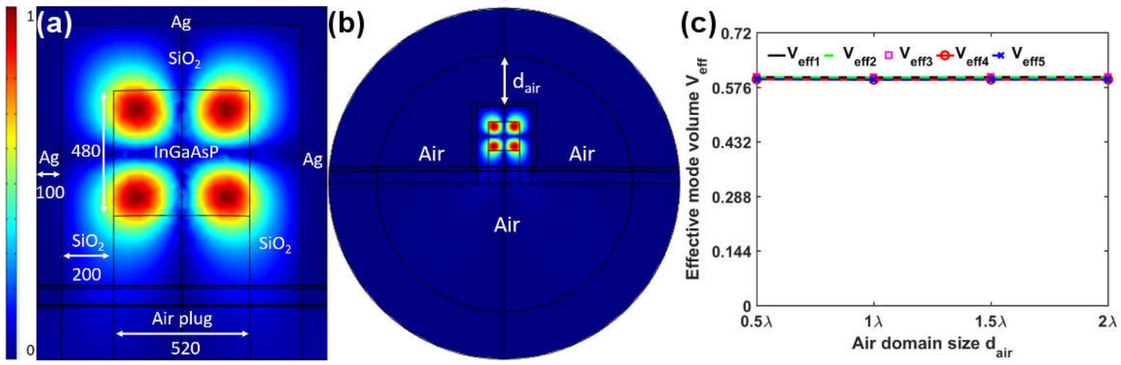
3.1. Metallo-Dielectric Resonator

We first present results on the evaluation of different Veff expressions for the Ag-cladded metallo–dielectric cavity. As the dielectric (SiO2) cladding (200 nm) between cavity core (InGaAsP) and cavity shell (Ag) is thick enough, the cavity supports well confined photonic modes, and the electric fields outside the active region quickly converge to zero. Therefore, we anticipate minor variation in the resulting Veff values with respect to change of simulation domain size (dair) compared to cavities supporting leaky plasmonic modes, such as those in Section 3.2 and Section 3.3.
A cross section of the metallo–dielectric cavity is shown in Figure 1a, where |E(r)| of the TE012 mode is plotted. It is apparent that the optical mode mostly overlaps with the InGaAsP active region. Further, because the ratio of relative permittivity of InGaAsP to SiO2 is (nInGaAsP/nSiO2)2 ≈ (3.4/1.45)2 = 5.5, the concentration of energy in the active region can be found by scaling the color plot of Figure 1a by a magnification factor of 5.5. This will lead to a confinement factor as given by Equation (3) close to unity. The simulation domain for the metallo–dielectric cavity is shown in Figure 1b, where we use a surrounding air region of variable characteristic length, dair. Figure 1c shows the Veff values of the five Veff expressions listed in Section 2 as a function of dair, with the latter ranging from 795 nm to 3180 nm, or from about half of the upper photoluminescence (PL) boundary of InGaAsP to two times of it. For the metallo–dielectric cavity, among all five Veff expressions, Veff,1,2,3 expressions yield an identical result, and Veff,4,5 expressions show a slightly smaller value due to the surface and PML integral terms added to the norm. The maximum difference between Veff,1,2,3 and Veff,4,5 is only 1.12%, which agrees with our analysis in Section 2. The dependence of Veff on dair is seen to be negligible, and the small variation is most likely attributable to the different meshes that are generated upon changing dair and not related to any physical features of the modal profile.

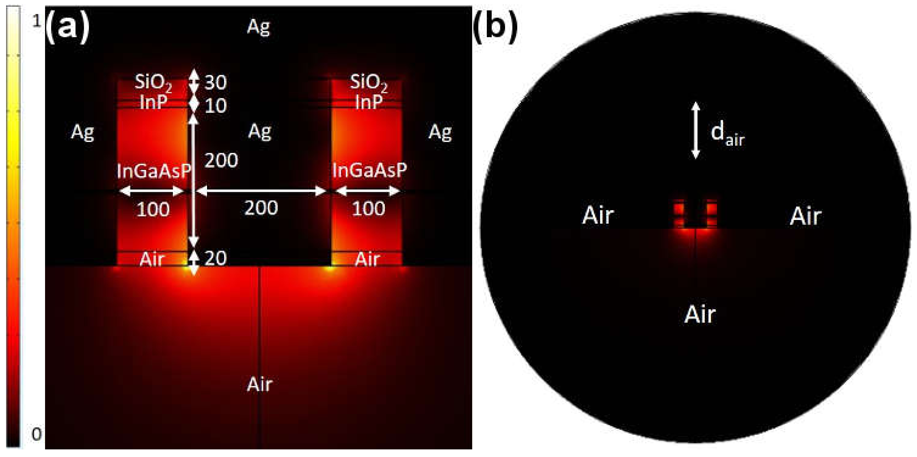
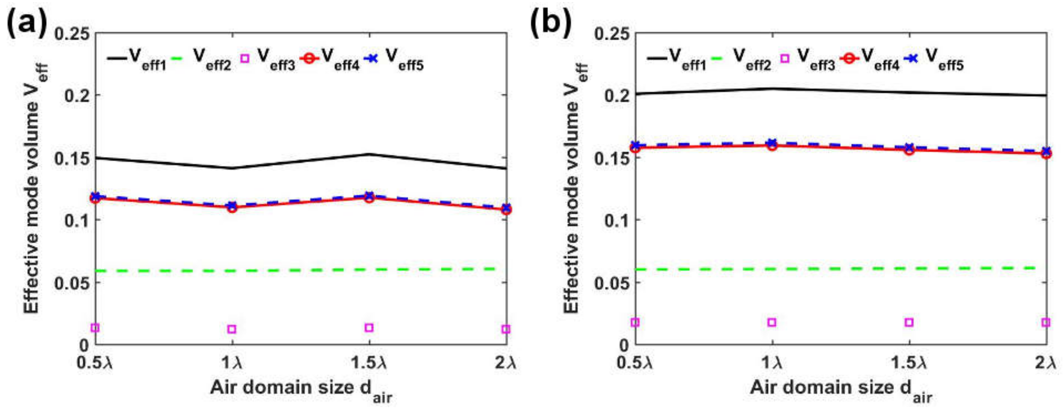
3.2. Coaxial Resonator with Ag

A cross section of the Ag-cladded coaxial cavity is shown in Figure 2a, where |E(r)| of the transverse electro-magnetic-like (TEM-like) mode is plotted. The cavity is enclosed by a spherical simulation space shown in Figure 2b. Despite the fact that the optical mode is fairly well confined to the active region of the cavity, there is notably more leakage into the air plug compared to the metallo–dielectric cavity. As a result, the electric field antinode is located in the air plug rather than the active region of the cavity. The quality factor of this plasmonic mode in the coaxial cavity is on the order of 100, which is about an order of magnitude lower than the photonic mode in the metallo–dielectric cavity.
The evaluated effective modal volumes of the Ag-cladded coaxial cavity are shown in Figure 3, for various simulation conditions, which include different meshing finesse and simulation domain sizes. As the electric field maxima and electric field energy density maxima located in the air region and active region respectively, Veff,3 has the largest denominator among all five Veff expressions. Therefore, Veff,3 exhibits the smallest values. As Veff,2 takes the electric field energy density in its denominator, this Veff expression is less sensitive to the change of simulation domain size, and is the most stable one. Among the other three expressions, as the field quickly vanishes at the simulation boundary, Veff,1, Veff,4 and Veff,5 all show converging values with less than 30% variation (Veff,1 ≈ 1.29 Veff,4 and 1.27 Veff,5) for all simulation conditions. From Figure 2a, it is apparent that the maximum electric field resides in the air region, which leads to a denominator for Veff,1, Veff,4 and Veff,5 that is significantly smaller than the denominators of both Veff,2 and Veff,3. Hence, the values of Veff,1, Veff,4 and Veff,5 are significantly greater than those of Veff,2 and Veff,3. Due to this same reason, Veff,1, Veff,4 and Veff,5 are more sensitive to the change of simulation domain size compared to Veff,2. Comparing Figure 3a and Figure 3b, which present results for fine and normal meshing, respectively, we observe a rather negligible change in the evaluated expression of Veff,2. However, it is important to note that because Veff,1, Veff,3, Veff,4 Veff,5 are normalized with respect to the maximum electric field rather than to the maximum electric field energy density as in the case of Veff,2, if this maximum lies in the air domain, then the mesh size could play an important role. For example, this singularity of the field produced by the corners of the Ag core can be suppressed by reducing the mesh size [33]. Additionally, the accuracy of the simulation can be further improved by introducing the idea of subpixel smoothing of the isotropic dielectric function [34].

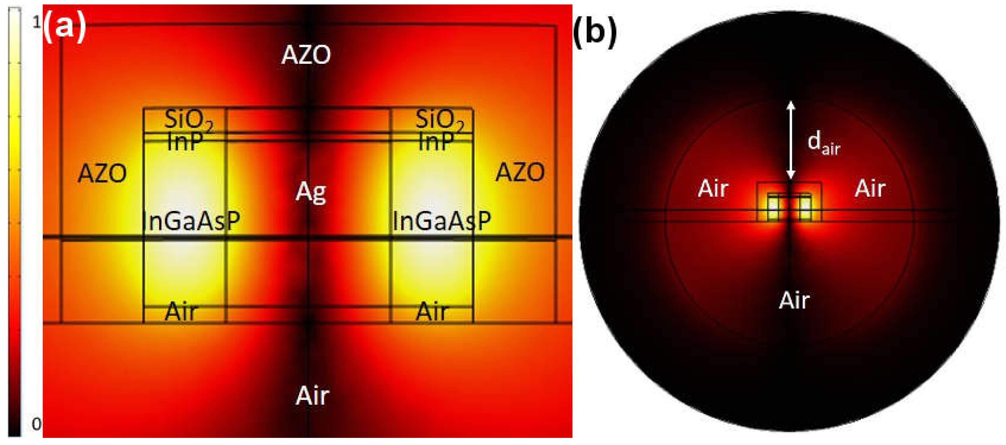
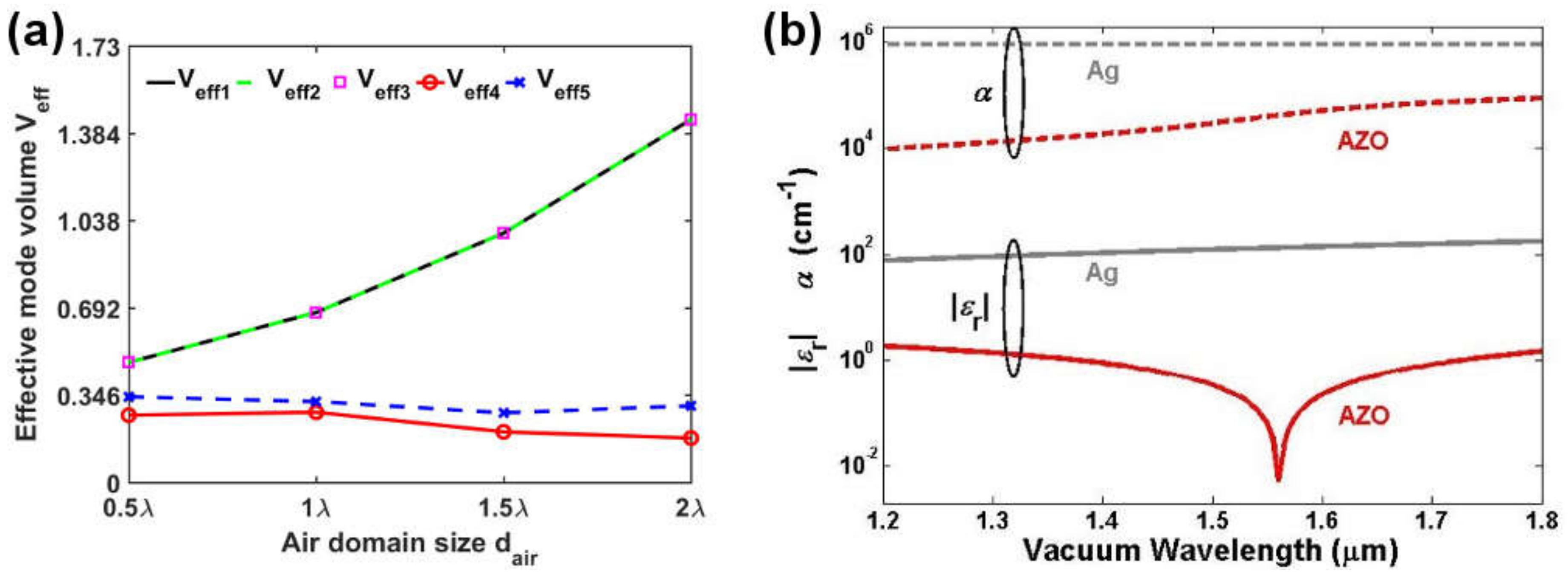
3.3. Coaxial Resonator with AZO

A cross section of the AZO-cladded coaxial cavity is shown in Figure 4a, along with the simulation space in Figure 4b. It is evident that the mode is rather poorly confined to the active region with a substantial portion of modal energy escaping the cavity. Hence, this cavity functions more as an optical antenna with a quality factor on the order of 10, one and two orders of magnitude smaller than the coaxial cavity with Ag and the metallo-dielectric cavity, respectively.
The evaluated effective modal volumes of the AZO–coaxial cavity are shown in Figure 5a, for various simulation conditions. These conditions include the spherical air domain of varying dair values. Veff,1, Veff,2, and Veff,3 yield diverging and identical results, increasing nonlinearly as dair increases from 0.5λ to 2.0λ, thus these three Veff do not have a well-defined value. On the contrary, Veff,4 and Veff,5 show converged Veff values. The converged effective modal volume values are attributed to the surface integration term in Equation (10) and the PML integration term in Equation (14), which compensate the diverging volume integration term.
While AZO exhibits an attenuation coefficient one to two orders of magnitude smaller than that of Ag over the spectral range of emission of InGaAsP (see Figure 5b), the absolute value of the real part of the AZO permittivity is close to unity, which leads to more of the mode residing in AZO and thus leading to a spatially divergent field because of the impedance match with the surrounding air domains. Therefore, it becomes problematic to define the quasi-normal mode (QNM) norm with some integral of electromagnetic field over the entire space. In this sense, Veff,4 and Veff,5 provide a way for the normalization of QNM of low-Q cavities or plasmonic resonators, i.e., non-Hermitian systems.

4. Discussion

Based on the results, the type of cavity clearly affects the robustness of the various expressions of Veff found in the literature. To quantify the stability of a Veff expression, we use the maximum percentage difference, defined as:
Δ ( # )   = ( max | V e f f , ( # ) m V e f f , ( # ) n | V e f f , ( # ) m ) × 100 %
where m and n refer to different simulation conditions. All the evaluation results are tabulated in Table 3 for fair comparison of the five effective modal volume expressions.
If the cavity supports a well-confined photonic mode, the electric field maximum resides in the active region and the five expressions yield nearly identical results if numerical error can be eliminated. This is confirmed with the metallo–dielectric cavity, where we observed that Δ1 = Δ2 = Δ3 ≈ Δ4 ≈ Δ5 < 0.21% as the simulation domain size increases. This can be considered a negligible change.
For cavities supporting plasmonic modes, the proximity of the cavity resonance to the metal plasma frequency plays an essential role in determining the efficacy of the Veff expressions. For the Ag–coaxial cavity under fine meshing, Δ2 < 2.02%, suggesting it is the most robust expression. However, for the AZO cavity, Veff,1, Veff,2, and Veff,3 all diverge nearly at the same rate, while Veff,4,5 converge but oscillate around certain values. Therefore, based on their robustness performance, for confined mode Veff,2 is suggested; for leaky mode, Veff,4,5 are suggested to obtain a more precise effective modal volume value. In addition, the choice of the correct effective modal volume formula should rely on a solid physical understanding of where the light–matter interaction of interest is happening.
In addition, notice that all five Veff formulae shown here only calculate the electric energy in the physical domain (including cavity and background material). However, for metallic cavities, especially at room temperature in the near-IR regime, the significant absorption loss of plasmonic or hybrid modes will result in unequal electric and magnetic energy in the cavity. For example, in the Ag–coaxial cavity, the electric energy is usually two to five times greater than the magnetic energy in the same material region. Therefore, calculating only the electric energy in metallic cavities should be understood as an approximation, and the Veff formulae should be modified for plasmonic modes if greater accuracy is desired [15,16,21].

5. Conclusions

We have identified five expressions in the literature commonly used for calculating the effective modal volume of resonant cavities. We evaluated and compared these expressions in the context of several canonical geometries supporting photonic and plasmonic modes for near-infrared nanoscale light sources. These included a metallo-dielectric cavity and coaxial cavities with Ag and AZO as cladding material. In the metallo-dielectric cavity, the various Veff expressions yield the same result and are robust to simulation domain changes because the electric field maximum resides in the active region. In the coaxial cavity, the Veff expressions yield results of varying stability due to the electric field and electrical energy density maxima residing in different regions. For low Q coaxial cavities, QNMs are no longer of finite energy, so standard QNM normalization methods based on energy consideration cannot be applied because of the spatially diverging field at large distance. Therefore, only Veff,4 and Veff,5 yield non-diverging results. Because of the relation of the effective modal volume to important quantities of theoretical and practical interest, such as the Purcell factor and spontaneous emission factor, our work conveys important results on the utility of the effective volume technique and its limitations.

Author Contributions

Conceptualization, J.S.T.S. and Q.G.; Methodology, J.S.T.S. and X.L.; Software, X.L. and Z.L.; Validation, X.L.; Formal Analysis, X.L. and J.S.T.S.; Investigation, X.L., J.S.T.S. and Q.G.; Writing-Original Draft Preparation, J.S.T.S. and X.L.; Writing-Review & Editing, J.S.T.S. and Q.G.; Supervision, Q.G.

Funding

This work was supported in part by UT Dallas faculty start-up fund, in part by the Office of Naval Research Multidisciplinary Research Initiative (N00014-13-1-0678), the National Science Foundation (NSF) (ECE3972 and ECCS-1229677), the NSF Center for Integrated Access Networks (EEC-0812072, Sub 502629), the Defense Advanced Research Projects Agency (N66001-12-1-4205) and the Cymer Corporation.

Conflicts of Interest

The authors declare no conflict of interest.

References

  1. Miller, D.A.B. Device requirements for optical interconnects to silicon chips. Proc. IEEE 2009, 97, 1166–1185. [Google Scholar] [CrossRef]
  2. Gu, Q.; Smalley, J.S.T.; Nezhad, M.P.; Simic, A.; Lee, J.H.; Katz, M.; Bondarenko, O.; Slutsky, B.; Mizrahi, A.; Lomakin, V.; et al. Subwavelength semiconductor lasers for dense chip-scale integration. Adv. Opt. Photonics 2014, 6, 1. [Google Scholar] [CrossRef]
  3. Purcell, E.M. Spontaneous Emission Probabilities at Radio Frquencies. Phys. Rev. 1946, 69, 674. [Google Scholar] [CrossRef]
  4. Li, X.; Gu, Q. Ultrafast shifted-core coaxial nano-emitter. Opt. Express 2018, 26, 15177–15185. [Google Scholar] [CrossRef] [PubMed]
  5. Lau, E.K.; Lakhani, A.; Tucker, R.S.; Wu, M.C. Enhanced modulation bandwidth of nanocavity light emitting devices. Opt. Express 2009, 17, 7790. [Google Scholar] [CrossRef] [PubMed]
  6. Khajavikhan, M.; Simic, A.; Katz, M.; Lee, J.H.; Slutsky, B.; Mizrahi, A.; Lomakin, V.; Fainman, Y. Thresholdless nanoscale coaxial lasers. Nature 2012, 482, 204–207. [Google Scholar] [CrossRef] [PubMed] [Green Version]
  7. Vahala, K.J. Optical microcavities. Nature 2003, 424, 839–846. [Google Scholar] [CrossRef] [PubMed]
  8. Chang, S.W.; Chuang, S.L. Fundamental formulation for plasmonic nanolasers. IEEE J. Quantum Electron. 2009, 45, 1014–1023. [Google Scholar] [CrossRef]
  9. Smalley, J.S.T.; Vallini, F.; Gu, Q.; Fainman, Y. Amplification and Lasing of Plasmonic Modes. Proc. IEEE 2016, 104, 2323–2337. [Google Scholar] [CrossRef]
  10. Balanis, C.A. Advanced Engineering Electromagnetics, 2nd ed.; John Wiley & Sons Comp.: Hoboken, NJ, USA, 2012; ISBN 9780874216561. [Google Scholar]
  11. Snyder, A.W. Optical Waveguide Theory; Springer Science & Business Media: Berlin, Germany, 1983; ISBN 0412099500. [Google Scholar]
  12. Chang, S.W.; Chuang, S.L. Normal modes for plasmonic nanolasers with dispersive and inhomogeneous media. Opt. Lett. 2009, 34, 91–93. [Google Scholar] [CrossRef] [PubMed]
  13. Johnson, P.B.; Christy, R.W. Optical constants of the noble metals. Phys. Rev. B 1972, 6, 4370–4379. [Google Scholar] [CrossRef]
  14. Novotny, L.; Hecht, B. Principles of Nano-Optics; Cambridge University Press: Cambridge, UK, 2009; Volume 9781107005, ISBN 9780511794193. [Google Scholar]
  15. Oulton, R.F.; Bartal, G.; Pile, D.F.P.; Zhang, X. Confinement and propagation characteristics of subwavelength plasmonic modes. New J. Phys. 2008, 10, 105018. [Google Scholar] [CrossRef]
  16. Zhang, Q.; Li, G.; Liu, X.; Qian, F.; Li, Y.; Sum, T.C.; Lieber, C.M.; Xiong, Q. A room temperature low-threshold ultraviolet plasmonic nanolaser. Nat. Commun. 2014, 5, 4953. [Google Scholar] [CrossRef] [PubMed] [Green Version]
  17. Gao, J.; McMillan, J.F.; Wu, M.C.; Zheng, J.; Assefa, S.; Wong, C.W. Demonstration of an air-slot mode-gap confined photonic crystal slab nanocavity with ultrasmall mode volumes. Appl. Phys. Lett. 2010, 96, 051123. [Google Scholar] [CrossRef] [Green Version]
  18. Bahari, B.; Tellez-Limon, R.; Kante, B. Directive and enhanced spontaneous emission using shifted cubes nanoantenna. J. Appl. Phys. 2016, 120, 093106. [Google Scholar] [CrossRef] [Green Version]
  19. Gérard, J.M.; Gayral, B. Strong Purcell effect for InAs quantum boxes in three-dimensional solid-state microcavities. J. Lightware Technol. 1999, 17, 2089–2095. [Google Scholar] [CrossRef]
  20. Kristensen, P.T.; Van Vlack, C.; Hughes, S. Generalized effective mode volume for leaky optical cavities. Opt. Lett. 2012, 37, 1649. [Google Scholar] [CrossRef] [PubMed]
  21. Sauvan, C.; Hugonin, J.P.; Maksymov, I.S.; Lalanne, P. Theory of the spontaneous optical emission of nanosize photonic and plasmon resonators. Phys. Rev. Lett. 2013, 110. [Google Scholar] [CrossRef] [PubMed]
  22. Nezhad, M.P.; Simic, A.; Bondarenko, O.; Slutsky, B.; Mizrahi, A.; Feng, L.; Lomakin, V.; Fainman, Y. Room-temperature subwavelength metallo-dielectric lasers. Nat. Photonics 2010, 4, 395–399. [Google Scholar] [CrossRef]
  23. Riley, C.T.; Smalley, J.S.T.; Post, K.W.; Basov, D.N.; Fainman, Y.; Wang, D.; Liu, Z.; Sirbuly, D.J. High-Quality, Ultraconformal Aluminum-Doped Zinc Oxide Nanoplasmonic and Hyperbolic Metamaterials. Small 2016, 12, 892–901. [Google Scholar] [CrossRef] [PubMed]
  24. Hao, F.; Nordlander, P. Efficient dielectric function for FDTD simulation of the optical properties of silver and gold nanoparticles. Chem. Phys. Lett. 2007, 446, 115–118. [Google Scholar] [CrossRef]
  25. Smalley, J.S.T.; Gu, Q.; Fainman, Y. Temperature dependence of the spontaneous emission factor in subwavelength semiconductor lasers. IEEE J. Quantum Electron. 2014, 50, 175–185. [Google Scholar] [CrossRef]
  26. Joannopoulos, J.J.D.; Johnson, S.; Winn, J.N.J.; Meade, R.R.D. Photonic Crystals: Molding the Flow of Light; Princeton University Press: Princeton, NJ, USA, 2008; ISBN 9780691124568. [Google Scholar]
  27. Smalley, J.S.T.; Vallini, F.; Kanté, B.; Fainman, Y. Modal amplification in active waveguides with hyperbolic dispersion at telecommunication frequencies. Opt. Express 2014, 22, 21088–21105. [Google Scholar] [CrossRef] [PubMed]
  28. Kristensen, P.T.; Hughes, S. Modes and Mode Volumes of Leaky Optical Cavities and Plasmonic Nanoresonators. ACS Photonics 2014, 1, 2–10. [Google Scholar] [CrossRef]
  29. De Ceglia, D.; Vincenti, M.A.; Grande, M.; Bianco, G.V.; Bruno, G.; D’orazio, A.; Scalora, M.; Ceglia, D. Tuning infrared guided-mode resonances with graphene. J. Opt. Soc. Am. B 2016, 33, 426. [Google Scholar] [CrossRef]
  30. Lalanne, P.; Yan, W.; Vynck, K.; Sauvan, C.; Hugonin, J.P. Light Interaction with Photonic and Plasmonic Resonances. Laser Photonics Rev. 2018, 12, 1700113. [Google Scholar] [CrossRef]
  31. Filter, R.; Słowik, K.; Straubel, J.; Lederer, F.; Rockstuhl, C. Nanoantennas for ultrabright single photon sources. Opt. Lett. 2014, 39, 1246. [Google Scholar] [CrossRef] [PubMed] [Green Version]
  32. Kelkar, H.; Wang, D.; Martín-Cano, D.; Hoffmann, B.; Christiansen, S.; Götzinger, S.; Sandoghdar, V. Sensing nanoparticles with a cantilever-based scannable optical cavity of low finesse and sub- λ3 volume. Phys. Rev. Appl. 2015, 4. [Google Scholar] [CrossRef]
  33. Choi, H.; Heuck, M.; Englund, D. Self-Similar Nanocavity Design with Ultrasmall Mode Volume for Single-Photon Nonlinearities. Phys. Rev. Lett. 2017, 118. [Google Scholar] [CrossRef] [PubMed]
  34. Oskooi, A.F.; Kottke, C.; Johnson, S.G. Accurate finite-difference time-domain simulation of anisotropic media by subpixel smoothing. Opt. Lett. 2009, 34, 2778. [Google Scholar] [CrossRef] [PubMed] [Green Version]
Figure 1. (a) Closeup of the transverse electric (TE) TE012 mode in the metallo-dielectric cavity (lengths expressed in nm) (b) Entire simulation space for the metallo–dielectric cavity (c) Veff as a function of dair evaluated for the various expressions. All of the traces overlap. (Q = 2700.8 at 2.0169e14 Hz (λ0 = 1486.4 nm).)
Applsci 08 01464 g001
Figure 2. (a) Closeup of the TEM-like mode of the coaxial cavity with Ag as cladding material (lengths expressed in nm). (b) Side view of the entire spherical simulation space for the coaxial cavity. (Q = 79.074 at 2.0542e14 Hz (λ0 = 1459.4 nm)).
Applsci 08 01464 g002
Figure 3. Effective modal volume of the coaxial cavity using Ag as metal for various simulation conditions, using (a) fine meshing and (b) normal meshing. λ = 1590 nm, which corresponds to the upper boundary of emission bandwidth of InGaAsP. Note that the traces for Veff,4 and Veff,5 are nearly identical.
Applsci 08 01464 g003
Figure 4. (a) Closeup of the mode of the coaxial cavity with AZO (aluminum-doped zinc oxide) as cladding material (dimensions of all material regions are identical to coaxial cavity with Ag). (b) Side view of entire spherical simulation space. (Q = 6.6884 at 2.2991e14 Hz (λ0 = 1304.0 nm).)
Applsci 08 01464 g004
Figure 5. (a) Effective modal volume of the coaxial cavity using AZO as a metal for various air domain size dair. (b) Absolute value of the real part of the relative permittivity |εr| (solid curves) and attenuation coefficient α (dashed curves) of Ag (gray curves) and AZO (red curves) as functions of vacuum wavelength.
Applsci 08 01464 g005
Table 1. Mode features of investigated nanoscale cavities. (AZO: aluminum-doped zinc oxide.)
Metallo–Dielectric Cavity with AgMetallic Coaxial Cavity with AZOMetallic Coaxial Cavity with Ag
Photonic Modexx
Plasmonic Mode x
Confined Modex x
Leaky Mode x
Table 2. PML and meshing conditions in eigenfrequency study.
FineNormal
PMLTypeSweepSweep
Number of layers105
CavityTypeFree tetrahedral (extremely fine)Free tetrahedral (fine)
Maximum element size (nm)λL/(6·nInGaAsP)λL/(4·nInGaAsP)
BackgoundTypeFree tetrahedral (normal)Free tetrahedral (normal)
Maximum element size (nm)λL/(6·nair)λL/(4·nair)
Metal-dielectric boundaryTypeFree tetrahedral (extremely fine)Free tetrahedral (extra fine)
Maximum element size (nm)1020
Table 3. Evaluation of Veff robustness using maximum percentage difference.
Maximum Percentage Difference (%)Cavity Types
Effective modal volume expressionsMetallo-dielectricCoaxial-Ag (normal/fine)Coaxial-AZO
Veff,10.212.748.03202.32
Veff,20.212.022.90202.32
Veff,30.212.748.03202.32
Veff,40.184.248.7957.98
Veff,50.184.308.8622.99

