All-Dielectric Metasurfaces with High-Fluorescence-Enhancing Capability


National Institute for Materials Science (NIMS), 1-1 Namiki, Tsukuba 305-0044, Japan
Appl. Sci. 2018, 8(8), 1328; https://doi.org/10.3390/app8081328
Submission received: 10 July 2018
/
Revised: 7 August 2018
/
Accepted: 7 August 2018
/
Published: 9 August 2018
(This article belongs to the Special Issue Photonic Metamaterials)
Abstract
:Featured Application
Metasurfaces in this article have a potential application for fluorescence sensing of biomarker molecules.
Abstract
All-dielectric metasurfaces are an emerging subfield in photonics. Light-wave manipulation has been extensively explored in these metasurfaces. Although light–matter interaction has also been investigated in these metasurfaces, only a limited number of studies have been reported to date. Here, we employ Si-rod-array metasurfaces to examine their fluorescence-enhancing capability. They were designed to have prominent resonances at the working wavelengths of fluorescent molecules. As a result, we experimentally observed significant fluorescence intensity enhancement, exceeding 1000-fold for a reference substrate that was a non-enhancing, flat Si wafer. Thus, we conclude that the all-dielectric metasurfaces can potentially serve as highly fluorescence-enhancing platforms. Their performance is comparable to the best performance reported for metallic metasurfaces. These results strongly suggest that all-dielectric metasurfaces can contribute to fluorescence-sensing of diverse molecules, including biomolecules.
1. Introduction
Metamaterials have stimulated significant research activity in the field of metallic micro- and nanostructures, from the viewpoints of their exotic electromagnetic responses, including magnetic resonance [1] and negative refraction effect [2,3]. Generally, three-dimensional photonic metamaterials operating at optical wavelengths are in high demand in nanofabrication, except for multilayer structures [4,5,6,7,8,9]. Therefore, photonic metamaterials in experiment have been mostly limited to single-layer or a-few-layer stacking structures [10,11]. Photonic metamaterials working at optical wavelengths have been extensively investigated to realize unconventional or extreme optical constants [12,13,14,15,16,17,18,19,20,21,22], such as a negative refractive index. They were mostly designed and fabricated using noble metals, such as gold [12,13,14] and silver [15,16,17,18,19,20,21,22].
Recently, metasurfaces which were originally conceived as single-layered metallic structures [23,24,25] have been attracting great interest. To date, the diversity includes a-few-layer surface structures on or connected to bulk substrates [26,27,28,29,30,31,32,33]. Many of the numerous papers on metasurfaces have been complied in review papers [34,35]. The single-layer metasurfaces tend to have more elaborated structures than most photonic metamaterials reported so far.
Currently, all-dielectric metasurfaces are a significant subgroup of metasurfaces [36]. One of their features is a series of Mie resonances induced in high refractive index nanostructures [37,38]. Thus, these metasurfaces were found rich in their physical properties. Further diverse optical functions, such as phase-and-polarization control [39], flat lenses [40,41,42,43], and holograms [44,45], have been realized based on the dielectric metasurfaces.
In addition to the search for novel optical devices and light-wave manipulation, light–matter interaction in artificial configurations has been attracting growing interest, ranging from fundamental investigations to practical applications. One of the practical issues is fluorescence (FL) enhancement because FL-intensity enhancement is directly linked to diverse FL-sensing applications in biotechnology. To date, several papers [46,47,48,49] have reported on highly successful FL-intensity enhancement exceeding two-thousand-fold in sparsely FL-molecule dispersed configurations, among the numerous papers on FL enhancement. These very large FL enhancements were achieved by exploiting metallic metasurfaces. To the best of our knowledge, there are no published reports on highly FL-enhancing dielectric metasurfaces in FL-molecule sparsely dispersed configurations. However, it was reported that photonic crystal slabs enabled hundred-fold FL enhancement [50], and that wavelength-selective photoluminescence (PL) extraction from semiconductor quantum dots (QDs) can be very effective in a dielectric metasurface [51]; thus, an opportunity exists to explore highly FL-enhancing dielectric metasurfaces. Here, we aim at examining Si-rod-array metasurfaces in terms of FL enhancement. We note that, at present, there is no theory that is able to predict highly FL-enhancing artificial nanostructures; therefore, experimentis the most direct and reliable way to find them.
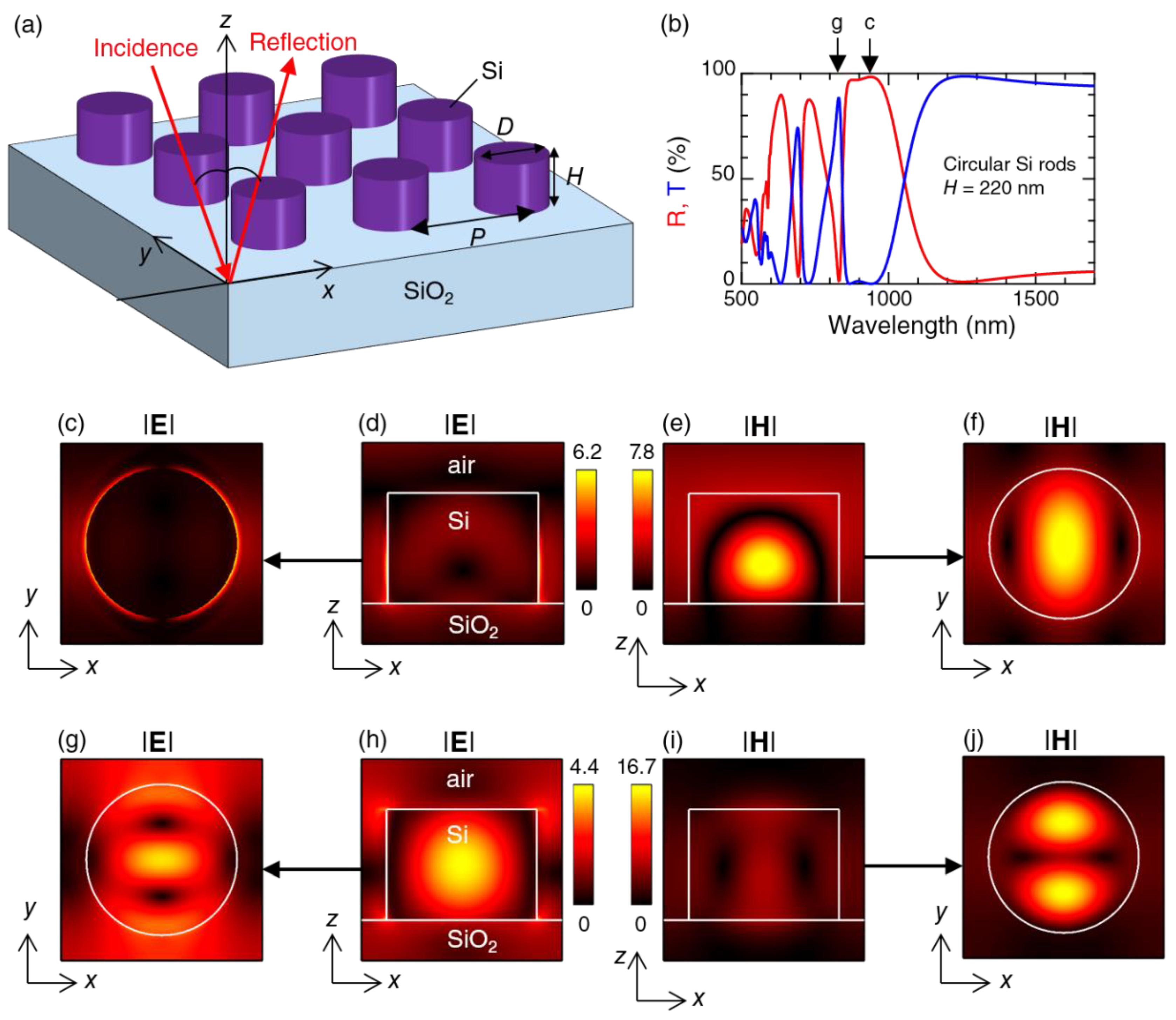
Before delving into the details of this investigation, we begin by describing the typical properties of a Si-rod-array metasurface, and briefly survey the main characteristics. Figure 1 illustrates a typical metasurface of cylindrical Si rods with Mie resonances [52,53]. Figure 1a illustrates a metasurface on a SiO2 substrate that is transparent in the wavelength range of interest. The unit structure is a cylindrical Si rod of diameter D and height H, and arrayed with a periodic length P in a square lattice. The periodic length P is defined to be the center-to-center distance between the nearest-neighbor Si rods. As shown in Figure 1a, the incident light is set to come from the top region of air in the xz plane.
Figure 1b shows numerically computed reflectance (R) and transmittance (T) spectra at a normal incidence. The spectra were calculated for a metasurface of P = 400 nm, D = 300 nm, and H = 220 nm, and shown with red and blue curves, respectively. In the wavelength range beyond 1200 nm, T is dominant, and R is suppressed, meaning that the metasurface is anti-reflective. As the wavelength becomes shorter, a fairly broad high-R band appears at 860–950 nm, and T is suppressed. In the shorter wavelength region than the high-R band, high-T, and high-R peaks alternatively appear in 600–840 nm. Next, we examine electromagnetic (EM) modes at the high-R and high-T wavelengths indicated by the arrows labeled c and g, respectively.
Figure 1c–j shows the EM-field distributions on resonances indicated by the arrows in Figure 1b. Figure 1c,d represents absolute value of the electric field |E| at 939.7 nm, which is a resonant wavelength of the high-R peak indicated by the arrow labeled c in Figure 1b. The xy- and xz-section |E| distributions are shown in Figure 1c,d, respectively. The z position of the xy section in Figure 1c is indicated by a black arrow from Figure 1d. The scale bar of the |E| is shown at the right-hand side of Figure 1d, and is in common to Figure 1c. Incident |E| was set to unity. Thus, it is found that resonantly, several-fold enhanced |E| is strongly localized at the sidewall of the Si rod.
Figure 1e,f shows the absolute value of the magnetic field |H|, corresponding to Figure 1c,d. The xz- and xy-section |H| are shown in Figure 1e,f, respectively. It is clear that the magnetic field is strongly localized and enhanced in the Si rod. The maximum value of |H| is 7.8 for the incident |H| = 1, meaning that the intensity |H|2 exceeds 60. Thus, the |E| and |H| distributions in Figure 1c–f indicate that the resonant mode is a magnetic dipole mode, which is understood as a Mie resonance.
Figure 1g–j exhibits resonant EM-field distributions at 831.3 nm, which is indicated by the arrow g in Figure 1b. The presentations are similar to those in Figure 1c–j. The resonant EM-field distributions exhibit electric dipole mode in the Si rod. In particular, one of the features of the electric dipole mode is that the maximum value of |H| is 16.7, and therefore, the intensity |H|2 exceeds 270, meaning the extreme magnetic-field enhancement. Thus, the R dip and T peak at the longest wavelength of 831.3 nm represent a Mie resonance of the electric-dipole type.
From these EM-field analyses for the Si-rod-array metasurface in Figure 1a, we found that high-R modes originate from magnetic multipole modes, and that high-T modes originate from electric multipole modes or guided modes inside the Si rods. The origins of optical resonances in Si-rod-array metasurfaces are classified in similar manners. Further information on these two resonant EM modes and other higher resonances which appear in the shorter wavelength range are shown in the Supplementary Materials (Figures S1–S4). Qualitatively, in this wavelength range of 600–1000 nm, we can classify the high-R modes into magnetic resonances and high-T (or low-R) modes into electric-dipole or guided modes in the Si rods. The qualitative understanding of the Si-rod-array metasurface is helpful to grasp optical spectra, such as R spectra, in experiments.
2. Materials and Methods
2.1. Fabrication of Si-Rod-Array Metasurfaces
The metasurfaces in this article were fabricated using silicon-on-insulator (SOI) substrates. We employed two types of SOI substrates; one had a SOI layer of 200 nm thickness and a buried oxide (BOX) layer of 400 nm thickness on a bulk Si wafer; the other had a 340 nm SOI layer and a 1000 nm BOX layer on a bulk Si wafer. Note that the SOI is crystalline Si, and that the atomic element of the BOX is SiO2. Electron-beam lithography (EBL) was performed on the EBL substrates and produced a resist mask for the BOSCH process, which is able to etch only the SOI layer in a very anisotropic and selective way, and produces Si rods of the same height to the SOI-layer thickness. The etching procedure was previously reported [54]. After the BOSCH process, the remaining resist mask was removed using O2 plasma.
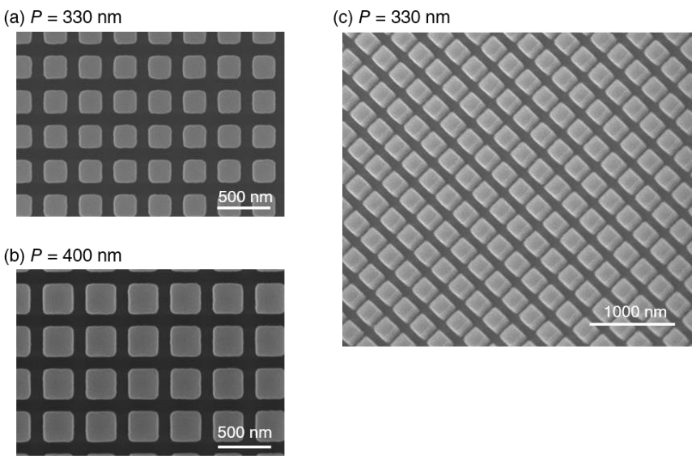
Figure 2 shows scanning electron microscope (SEM) images of the representative metasurfaces, which were fabricated using the substrates of a 200 nm SOI layer. Figure 2a,b shows the top-view SEM images of the metasurfaces of periodic lengths P = 330 and 400 nm, respectively. The corner-round squares are the Si rods. We note that exact squares are extremely difficult to fabricate using the standard EBL. The gaps between the Si rods are approximate 110 and 108 nm in Figure 2a,b, respectively. The white bars in Figure 2a,b represent a distance of 500 nm. Figure 2c shows an oblique-view SEM image of the metasurface in Figure 3a, suggesting that the etching of the SOI layer successfully produced rectangular Si rods as intended.
We mention the reasons why we chose SOI substrates in this study. One is practical; we employed SOI substrates in the previous experiments [29,48,49,50], and therefore, could use them at once. The other is that we preferred the relatively smaller optical loss in crystalline SOI than in amorphous Si films grown on transparent substrates such as SiO2. A disadvantage of using SOI substrates is that light absorption is relatively difficult to evaluate, compared to the configuration using Si films on SiO2 substrates. However, light absorption is not a key issue in this study.
Also, we note that the difference in R spectra of Si-rod-array metasurfaces based on SOI substrates, and of the metasurfaces in Figure 1, is small in the wavelength range of interest. The R spectra are shown in the Supplementary Materials (Figure S5).
2.2. Optical Measurement
R spectra were measured in a wide range from 500 to 1600 nm by using a spectrometer with incident-angle-resolving unit (V7200, JASCO Corporation, Tokyo, Japan). The incident polarization was set to p or s polarizations. When the plane of incidence is set to the xz plane as shown in Figure 1a, p polarization is the incident electric-field vector Ein parallel tothe xz plane, whereas s polarization is Ein parallel to the y axis.
FL measurements were conducted in an illumination-and-collection setup. Incident laser light of wavelength 532 nm was emitted by a single-mode continuous-wave laser and was focused onto the metasurfaces. This laser light was focused using a 10× objective lens of numerical aperture 0.26. The typical incident laser power on the sample surface was 1.0 mW. FL emitted by rhodamine 590 (R590) molecules (Exciton Inc., Lockbourne, OH, USA) was collected using the objective lens, and was measured by a charge-coupled device camera attached to a monochromator. The exposure time in measuring the FL signals was 5 s.
The R590 molecules were dispersed on the metasurfaces as methanol solution. Typically, a 2 µL drop of the R590 solution of concentration 50 nM was dispersed on the metasurfaces, then run promptly over the metasurfaces, and dried within a few seconds. From the dispersed area, we estimated the average molecular density on the metasurfaces. In order to quantitatively evaluate the FL-intensity enhancement factor, we prepared a reference configuration using a flat Si wafer, on which the FL intensity of dispersed R590 molecules was far smaller than that on the metasurfaces, so that we dispersed 5 µM methanol solution of R590 molecules on the Si wafer and used the FL spectrum as a reference for normalizing experimental conditions, that is, the dispersed molecular density and the optical measurement condition. We note that the reference FL spectrum went through a smoothing process on graphical software to definitely evaluate the FL-intensity enhancement; as a result, the reference spectrum looks smoother, at a glance, than the FL spectra on the metasurfaces, which does not imply a better signal-to-noise ratio in the reference spectrum.
2.3. Numerical Method
The optical properties of the metasurfaces were analyzed using a computational code combining rigorous coupled-wave analysis (RCWA) method [55] with a scattering-matrix (S-matrix) algorithm [56]. The RCWA method is based on Fourier representation of Maxwell equations, and is a rigorous method in electromagnetism. This method had been impractical for a long time because of the very slow convergence, and became practical for arbitrary periodic structures, including metals, by the finding of the inverse Fourier factorization algorithm in 1996 [57]. The RCWA–S-matrix code is particularly suitable for numerical calculations for optical spectra, such as reflection and transmission in arbitrary periodic structures. The code was numerically executed on supercomputers in a multi-parallel implementation (MPI) manner, and the R spectra were evaluated. Owing to the MPI parallelization, the calculation time for the R spectra was substantially reduced. Resonant EM fields were also evaluated using the RCWA-S-matrix code. The R spectra and EM fields in this article were thus obtained.
To implement realistic computations, we used material parameters in the literature that compiled measured data or representative values. The complex refractive index of Si was taken from [58]. The refractive indices of air and SiO2 were set to 1.00027 and 1.46, respectively, in the range of present interest.
3. Results
3.1. Enhanced FL Measurement
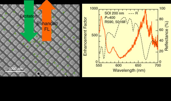
Figure 3 shows a series of enhanced FL of the R590 molecules dispersed on the three types of Si-rod-array metasurfaces. The left-hand-side column in Figure 3 displays the measured FL (colored curves) and R (black dashed curves) spectra; in addition, the reference FL spectrum of the R590 molecules dispersed on a flat Si wafer is shown, for normalized experimental conditions, with the black solid curve multiplied by a fixed factor for clarity. We note that the R spectra are plotted for the right axes. The right-hand-side column in Figure 3 presents the FL-intensity enhancement factors (colored curves), which are defined as the ratio of the FL intensity on the metasurface to the reference FL intensity in each panel of the left-hand-side column.
The enhanced FL spectrum of the R590 molecules (green curve) on the metasurface of a SOI of 200 nm thickness and P = 330 nm are shown in Figure 3a. The measured R spectrum is shown with the black dashed line; it was measured at an incident angle of 5° and p polarization. The reference FL spectrum is shown with a normalization based on the experimental conditions, and with an enlargement of 100-fold for clarity. It is evident that the FL is significantly enhanced at 590 nm, which corresponds to one of the R peaks. Note that the original FL peak of the R590 molecules is located at about 565 nm, as can be seen in the reference spectrum. Thus, the large FL enhancement takes place together with an evident spectral change. Such spectral changes were found in the experiment exploiting high-emittance metasurfaces, including metallic nanostructures [48,49], suggesting that FL-emitting electronic transitions in the FL molecules are significantly modified through the coupling with the resonances in the metasurfaces. The FL-intensity enhancement factor (green curve) is shown in Figure 3b, evaluated from the FL spectra in Figure 3a. The most prominent peak of enhancement factor is approximate 950 at 590 nm. Besides, small peaks can be seen near the wavelengths of R peak and dips (approximately, 630, 650, and 670 nm). The R spectrum is shown again for comparison, being identical to that in Figure 3a.
The enhanced FL spectrum of the R590 molecules (orange curve) on the metasurface of an SOI of 200 nm thickness and P = 400 nm is shown in Figure 3c. The measured p-polarized R spectrum at 5°, and the reference FL spectrum, are shown in a similar manner to Figure 3a. The reference is enlarged by 50-fold. The FL signals were significantly enhanced, and the spectral shape is modified.
The FL-intensity enhancement factor (orange curve) is shown in Figure 3d, evaluated from the FL spectra in Figure 3c. The largest peak corresponds to the deep R dip and is located at 668 nm, showing 1000-fold intensity enhancement. The second largest peak at 556 nm correspond to a small R peak.
The enhanced FL spectrum of the R590 molecules (blue curve) on the metasurface of an SOI of 340 nm thickness and P = 400 nm is shown in Figure 3e. The measured p-polarized R spectrum at 5° and the reference FL spectrum are shown in a similar manner to Figure 3c. Four enhanced FL peaks appear, which mostly correspond to R dips.
3.2. Resonances on the Si-Rod Metasurfaces
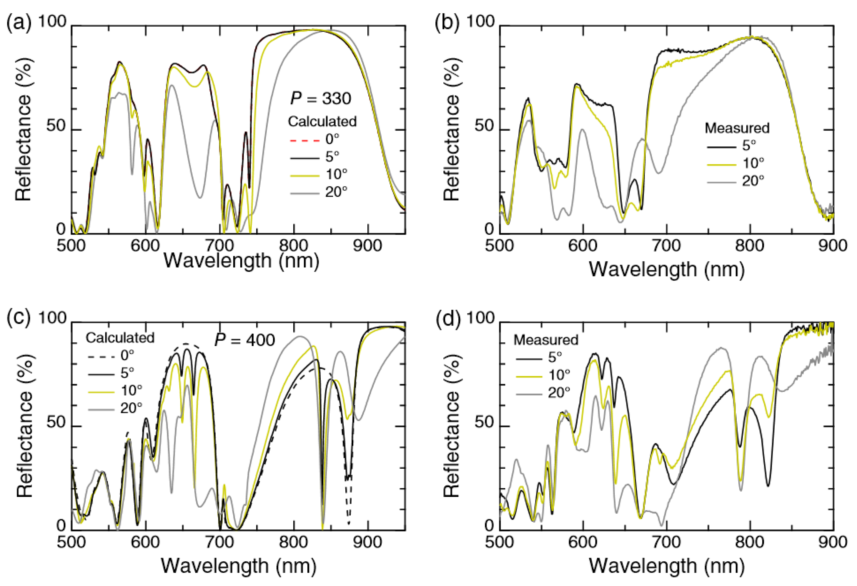
Figure 4 shows a series of R spectra for the Si-rod metasurfaces shown in Figure 2. Figure 4a,b show numerically calculated and measured R spectra, respectively, for the metasurface of a SOI of 200 nm thickness and P = 330 nm.
In Figure 4a, the simulated R spectra at incident angles of 0°, 5°, 10°, and 20° are shown with red dotted, black solid, yellow solid, and gray solid curves, respectively. The incident polarization was set to be p polarization. We note that the R spectra at 0° and 5° are quite similar and almost overlap. The simulation was implemented to model the actual metasurface in Figure 2a by assuming that the Si rod is a square-shaped rod from the top view.
In Figure 4b, the R spectra were measured at incident angles of 5°, 10°, and 20°, shown similarly to Figure 4a. It is verified in Figure 4a,b that the highest-R band appears at 5° in the longer wavelength range around 800 nm, and the other two high-R bands appear at 5° in shorter wavelength range than the highest-R band.
A comparison between the measured R spectra and the simulated R spectra in Figure 4a,b revealed a qualitatively good agreement. The three high-R bands with R > 50% appear in both spectra. The high-R bands at the longest wavelength exhibit the widest band width among the three bands. As incident angles increase, the R tends to decrease in the wavelength range from 550 to 800 nm. Thus, several agreements are readily found. We note that the small deviation in the spectral shapes probably comes from structural difference between the actual metasurface in Figure 2a,c and the modeled metasurface of ideally rectangular Si rods in the simulation.
The numerically calculated and measured R spectra are respectively shown in Figure 4c,d for the metasurface of a SOI of 200 nm thickness and P = 400 nm. A qualitative good agreement is also found in this case. For example, (i) almost perfect R at the edge of long wavelength side appears in the calculated and measured spectra of incident angles of 10° and less. (ii) A high-R band around 650 nm in Figure 4c includes two asymmetric modes that appear as two R dips at 5° and more; the asymmetric modes were measured as shown in Figure 4d. We point out that the asymmetric modes do not contribute to the FL enhancement in Figure 3c,d. This is probably because the asymmetric modes do not match the symmetry of electric-dipole transitions resulting in the FL, and cannot couple with the electronic transitions.
The agreement between the simulation and measurement was found to be qualitatively better in Figure 4c,d than that in Figure 4a,b. This is partially because the actual metasurface is more similar in structure to the modeled metasurface in the simulation. Indeed, it is easily verified in the SEM images of Figure 2 that the Si rods of P = 400 nm resemble ideal squares in shape, compared with the Si rods of P = 330 nm.
3.3. Resonant EM Fields at the FL Enhancement
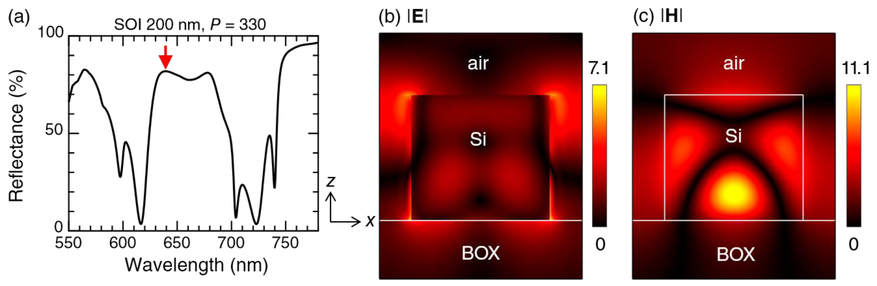
Figure 5 shows a set of resonant EM-field distributions that correspond to the peak of the enhancement factor in Figure 3b. Figure 5a shows the numerically calculated R spectrum at the normal incidence, which is also represented in Figure 4a, though it is overlapped with the R spectrum at 5°. The FL-enhancing wavelength corresponds to the red arrow (639.3 nm) in the high-R band, which was observed during the experiment (Figure 3a,b).
The |E| and |H| distributions in an xz-section view are respectively shown in Figure 5c,d at the wavelength indicated by the red arrow in Figure 5a. The xz-section was taken at the center of the Si rod. The resonantly enhanced electric fields mainly exist at the outer surface of the Si rod, whereas the resonant magnetic fields are dominantly localized in the Si rod, taking the maximum value of 11.1, and indicating significant field enhancement inside the Si rod. The magnetic-field distribution exhibits a multipole feature. Thus, these EM-field distributions indicate that the resonant mode is of a higher magnetic resonance in the Si rod.
Figure 6 shows the resonant EM-field distributions contributing to the FL enhancement of the metasurface of SOI-thickness 200 nm and P = 400 nm. The experimental data are shown in Figure 3c,d. Figure 6a shows, again, the numerically calculated R spectrum at the normal incidence, which has appeared in Figure 4c. The red arrows indicate the wavelengths corresponding to the peaks of the FL-intensity enhancement factor in Figure 3d.
In Figure 6b,c, the |E| and |H| distributions are shown in an xz-section view, respectively. They are excited at the R-dip wavelength (701.1 nm), which is indicated by the red arrow with label b,c in Figure 6a. The xz section was taken at the center of the Si rod. From the EM-field distributions, it is clear that the incident light efficiently propagates in the Si rod. The magnetic field dominantly exists inside the Si rod, and the electric field is strongly localized at the sidewall of the Si rod. The Si rod works as a waveguide at this wavelength. The EM-field distributions also indicate that they form a 1-wavelength guided mode; consequently, impedance matching is satisfied at the top and bottom interfaces of the Si rod, resulting in the low R (i.e., R dip). We also note that the field enhancement is particularly significant among the various resonant modes of the Si rods; the maxima of the electric- and magnetic-field intensity are 557 and 279, respectively, for the incident intensities of 1.
In Figure 6d,e, the |E| and |H| distributions are shown in the same xz views to Figure 6b,c, respectively, at the R-peak wavelength (576.3 nm) indicated by the red arrow with label d,e in Figure 6a. The EM-field distributions also indicate a waveguide mode in the Si rod, which forms a 3/2-wavelength mode. Thus, the resonant mode is a 3/2-wavelength guided mode. This mode does not have impedance matching at the interface of Si and BOX. As a result, the R cannot be small, and indeed forms a peak at the wavelength (Figure 5a).
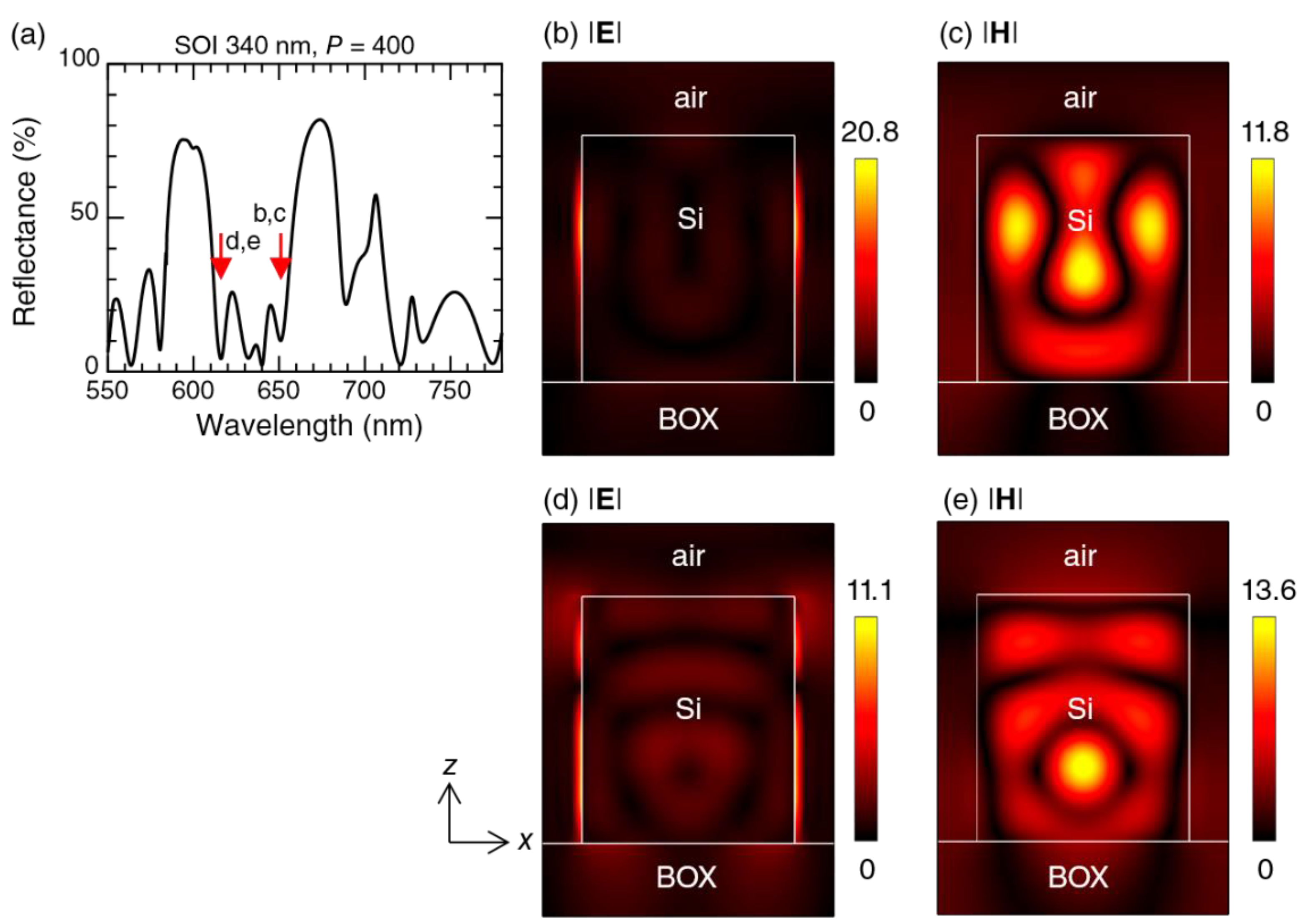
Figure 7 shows the resonant EM-field distributions that contribute to the FL enhancement in the metasurface of a SOI of 340 nm thickness and P = 400 nm. The corresponding experimental data are shown in Figure 3e,f. Figure 7a shows the numerically calculated R spectrum at the normal incidence. The wavelengths indicated by the red arrows correspond to the peaks of the FL enhancement factor in the experiment (Figure 3f).
In Figure 7b,c, the |E| and |H| distributions are shown in an xz-section view, respectively, at the R-dip wavelength (651.0 nm) indicated by the red arrow with label b,c in Figure 7a. The xz section was taken at the center of the Si rod. One of the noteworthy features is that the magnetic field is confined in the Si rod, whereas the enhanced electric field is strongly localized at the sidewall of the Si rod. Thus, we can attribute this mode to a higher magnetic mode. Note that it is not simply attributed to a multipole mode. This is partially because the height of the Si rod is fairly high for the effective wavelength inside the Si rod, and there is a degree of freedom to form three-dimensional complex EM modes.
In Figure 7d,e, the |E| and |H| distributions are shown in an xz-section view, respectively, at the R-dip wavelength (616.1 nm) indicated by the red arrow with label d,e in Figure 7a. The section was taken at the center of the Si rod. This resonant EM mode is also ascribed to a higher magnetic mode. The magnetic field forms a complicated distribution, and the electric field is mainly enhanced at the sidewall of Si rod.
Summarizing the results in Figure 5, Figure 6 and Figure 7, we realize that there is a tendency for the large FL-intensity enhancement factors to appear at resonant wavelengths associated with R peaks or dips at the normal incidence. The largest FL enhancement factor in Figure 3d was found at the 1-wavelength guided resonance in Figure 6b,c. The second largest FL enhancement factor in Figure 3b originates from a higher magnetic resonance in Figure 5. The third largest FL enhancement factor in Figure 3d was attributed to the 3/2-wavelength guided resonance in Figure 6d,e. A common feature of these three modes is that the enhanced electric-field intensity is strongly localized at the outmost surface of the Si rods. Thus, the resonant electric-field enhancement was identified as a key factor for the large FL enhancement factors. Further discussion is presented in the next section.
Also, strong magnetic fields were found in the Si rods, which have hundred-fold enhanced intensities compared to the incident magnetic-field intensity. Thus, when magnetic dipoles are properly placed inside the Si rods, significant magnetic-dipole emissions are expected to be observed. Rare-earth ions, such as Eu and Er, are candidates for magnetic-dipole emissions. Indeed, in a plasmonic structure, it was experimentally demonstrated that electric- and magnetic-dipoles are selectively enhanced at the positions where electric and magnetic fields are strong, respectively [59].
4. Discussion
Let us discuss the FL enhancement observed in this investigation. Considering the electric-field distribution in Figure 5b, the intensity |E|2 has the maximum value of 50.4 at the bottom of the Si rod, while the intensities at most of the outmost surfaces of the Si rod are estimated to be 10 or less. Therefore, although resonant electric-field enhancement is one of the origins of the large FL-intensity enhancement (~1000), it cannot fully account for the enhancement effect.
A similar situation to this study was found for metallic metasurfaces; in this case, the FL-intensity enhancement mechanism was examined by considering all the processes from the excitation to FL emission [48]. In the present dielectric metasurface, such full consideration is also necessary to account for the FL enhancement effect. Concretely, the enhancement factor (EF) is expressed such that
where and are excited populations in the metasurface and reference configurations, respectively; and are quantum yields of the FL molecules in the metasurface and reference configurations, respectively; and are radiative transition rates dependent on outgoing wavevector K in the metasurface and reference configurations, respectively. The transition rates are calculated, in principle, based on quantum mechanical transition probabilities. The subscripts enh and 0 denote the metasurface and reference configurations, respectively. We note that the quantum yield is represented with radiative and nonradiative transition rates, such as , where denotes the nonradiative transition rate. The EF in Equation (1) represents a generalized Purcell factor. Note that, when we consider an ideally simplified situation that a single two-level system is excited only once per unit time, the EF reduces into the original Purcell factor of [60], because of and . In comparison with the original Purcell factor, the EF in Equation (1) is substantially elaborated in accordance with the actual experimental configuration.
The EFs have been experimentally evaluated in Figure 3b,d,f, whereas it is extremely difficult to experimentally determine the constituent factors at the right-hand side of Equation (1). Therefore, we discuss the EF from the electric-field distributions evaluated in the computations. First, we refer to the excitation efficiency, which is proportional to the excited populations in Equation (1). We compared electric-field intensities at 532.0 nm on the outmost metasurfaces of the Si rods, at which the dispersed FL molecules were located, with those on the reference Si wafer; the electric fields are shown in the Supplementary Materials (Figure S6). As a result, we estimated the intensity ratio of to be 22 on average in the case of 200 nm SOI thickness and P = 400 nm (Figure 3c,d), where and denote electric-field vectors in the metasurface and reference, respectively. Thus, it is impossible to attribute the origin of the large EF up to 1000 only to the factor of . Second, definite spectral changes in the FL spectra in Figure 3 indicate that FL-emitting electronic transitions are modified in the metasurfaces; that is, the radiative-transition-rate ratio of is substantially modulated. Taking account of an averaged estimation above for , the ratio can take a value of approximately 50, if we assume that the quantum yield does not change significantly. Such a non-negligible value of the ratio is consistent with the experimental observations of the prominent FL-spectrum changes in Figure 3. We note that the ratio of includes the ratio of electric-field intensity at the FL-emitting wavelength; therefore, strong localization of resonant electric fields outside the Si rods are suitable to attain large EFs. Indeed, Figure 5, Figure 6 and Figure 7 show the electric-field localization at the outmost surface of the Si rods. In this sense, electric-dipole type resonance is considered to be unsuitable for large FL enhancement in this experiment. Also, note that the ratio depends on the outgoing vector K, being sensitive to directional emittance of the metasurfaces; thus, the emittance control is a key factor to obtain large EFs. Overall, the FL enhancement found in this study requires full consideration represented with Equation (1).
The present metasurfaces exhibit high capability of FL-intensity enhancement. Therefore, they are expected to be practical platforms for FL sensing. By incorporating proper immobilization techniques, a very low limit of detection for FL-labeled biomolecules can be assumed, as was conducted in the metallic metasurfaces [47].
In this study, FL signals are solely enhanced on the Si-rod-array metasurfaces. By contrast, the FL molecules dispersed on metallic metasurfaces tend to exhibit both FL and Raman-scattering signals in the metal-molecule direct contact configuration [49]. This is a distinct difference between dielectric and metallic metasurfaces. When self-assembled monolayers (SAMs) or other spacers are introduced onto the metallic metasurfaces, it was observed that the Raman-scattering signals disappear. Therefore, metal-molecule direct contact is most likely to affect electronic transition in the dispersed molecules. In the dielectric metasurfaces, such interplay does not take place. Very recently, hot electrons from metallic metasurfaces were reported to substantially contribute to the PL process in semiconductor QDs [61]. Thus, we suggest that hot electrons play a role in the metal-molecule contacting system.
So far, metallic (in particular, gold) metasurfaces have been considered to be one of the best candidates in the development of a practical FL-sensing platform. However, the present results strongly suggest that the dielectric metasurfaces can be a good candidate for these platforms. The dielectric metasurfaces with high-FL-enhancing capability will become a strong competitor to the metallic metasurfaces when a surface-improving protocol, such as SAMs, is established. The present metasurfaces have the advantage of a lower cost compared to the metallic metasurfaces, because of their gold-free structure.
5. Conclusions
The Si-rod-array metasurfaces were fabricated using two types of SOI substrates, and the optical qualities were assessed by the R-spectrum measurement. It was confirmed that the fabricated metasurfaces were well fabricated in accordance with their design. The all-dielectric metasurfaces were employed in the experiments on FL-intensity enhancement. We found experimentally that the metasurfaces have high capabilities to enhance FL signals at several EM resonances. The most prominent FL-intensity enhancement factor exceeds 1000-fold, which is almost comparable to the best metallic metasurfaces reported so far. The resonant EM modes were numerically examined, and it was determined that the guided modes and the higher magnetic modes in the Si rods efficiently contribute to the significant FL enhancement. The FL enhancement factor was discussed in detail using an extended Purcell factor (Equation (1)), which is suitable to describe this experimental configuration.
Supplementary Materials
The following are available online at https://www.mdpi.com/2076-3417/8/8/1328/s1. Figure S1: EM-field distributions at the magnetic-dipole resonance associated with the first R peak in Figure 1. Figure S2: EM-field distributions at the electric-dipole resonance at the first T peak (or R dip) in Figure 1. Figure S3: EM-field distributions at the 1-wavelength guided resonance associated with the second T peak (or R dip) in Figure 1. Figure S4: EM-field distributions at a higher magnetic resonance associated with the third R peak in Figure 1. Figure S5: Comparison of R spectra of the Si-rod-array metasurface and the SOI-based metasurface. Figure S6: |E| distributions at the excitation wavelength of 532.0 nm.
Funding
This research was partially funded by JSPS KAKENHI Grant (number JP17H01066) from the Japan Society for Promotion of Science and by the 4th mid-term research project in NIMS.
Acknowledgments
The numerical part in this research was supported by HPCI System Research Project (ID: hp180107), being implemented at Cyberscience Center, Tohoku University. Nanofabrication was conducted at Nanofabrication Platform and Namiki Foundry in NIMS. The author thanks Jun Matsuzawa for technical assistance in nanofabrication.
Conflicts of Interest
The author declares no conflict of interest.
References
- Pendry, J.B.; Holden, A.J.; Robbins, D.J.; Stewart, W.J. Magnetism from conductors and enhanced nonlinear phenomena. IEEE Trans. Microw. Theory Tech. 1999, 47, 2075–2084. [Google Scholar] [CrossRef] [Green Version]
- Pendry, J.B. Negative refraction makes a perfect lens. Phys. Rev. Lett. 2000, 85, 3966–3969. [Google Scholar] [CrossRef] [PubMed]
- Fang, N.; Lee, H.; Sun, C.; Zhang, X. Sub-diffraction-limited optical imaging with a silver superlens. Science 2005, 308, 534–537. [Google Scholar] [CrossRef] [PubMed]
- Liu, Z.; Lee, H.; Xiong, Y.; Sun, C.; Zhang, X. Far-field optical hyperlens magnifying sub-diffraction-limited objects. Science 2007, 315, 1686. [Google Scholar] [CrossRef] [PubMed]
- Rho, J.; Ye, Z.; Xiong, Y.; Yin, X.; Liu, Z.; Choi, H.; Bartal, G.; Zhang, X. Spherical hyperlens for two-dimensional sub-diffractional imaging at visible frequencies. Nat. Commun. 2010, 1, 143. [Google Scholar] [CrossRef] [PubMed] [Green Version]
- Xu, T.; Agrawal, A.; Abashin, M.; Chau, K.J.; Lezec, H.J. All-angle negative refraction and active flat lensing of ultraviolet light. Nature 2013, 497, 470–474. [Google Scholar] [CrossRef] [PubMed]
- Iwanaga, M. Hyperlens-array-implemented optical microscopy. Appl. Phys. Lett. 2014, 105, 053112. [Google Scholar] [CrossRef]
- Iwanaga, M. Toward super-resolution imaging at green wavelengths employing stratified metal-insulator metamaterials. Photonics 2015, 2, 468–482. [Google Scholar] [CrossRef]
- Byun, M.; Lee, D.; Kim, M.; Kim, Y.; Kim, K.; Ok, J.G.; Rho, J.; Lee, H. Demonstration of nanoimprinted hyperlens array for high-throughput sub-diffraction imaging. Sci. Rep. 2017, 7, 46314. [Google Scholar] [CrossRef] [PubMed] [Green Version]
- Solymar, L.; Shamonina, E. Waves in Metamaterials; Oxford University Press: Oxford, UK, 2009. [Google Scholar]
- Iwanaga, M. Plasmonic Resonators: Fundamentals, Advances, and Applications; Pan Stanford Publishing: Singapore, 2016. [Google Scholar] [CrossRef]
- Zhang, S.; Fan, W.; Panoiu, N.; Malloy, K.; Osgood, R.; Brueck, S. Experimental demonstration of near-infrared negative-index metamaterials. Phys. Rev. Lett. 2005, 95, 137404. [Google Scholar] [CrossRef] [PubMed]
- Shalaev, V.M.; Cai, W.; Chettiar, U.K.; Yuan, H.-K.; Sarychev, A.K.; Drachev, V.P.; Kildishev, A.V. Negative index of refraction in optical metamaterials. Opt. Lett. 2005, 30, 3356–3358. [Google Scholar] [CrossRef] [PubMed]
- Dolling, G.; Enkrich, C.; Wegener, M.; Soukoulis, C.M.; Linden, S. Low-loss negative-index metamaterial at telecommunication wavelengths. Opt. Lett. 2006, 31, 1800–1802. [Google Scholar] [CrossRef] [PubMed]
- Dolling, G.; Wegener, M.; Soukoulis, C.M.; Linden, S. Negative-index metamaterial at 780 nm wavelength. Opt. Lett. 2007, 32, 53–55. [Google Scholar] [CrossRef] [PubMed]
- Burgos, S.P.; de Waele, R.; Polman, A.; Atwater, H.A. A single-layer wide-angle negative-index metamaterial at visible frequencies. Nat. Mater. 2010, 9, 407–412. [Google Scholar] [CrossRef] [PubMed] [Green Version]
- Xiao, S.; Drachev, V.P.; Kildishev, A.V.; Ni, X.; Chettiar, U.K.; Yuan, H.K.; Shalaev, V.M. Loss-free and active optical negative-index metamaterials. Nature 2010, 466, 735–738. [Google Scholar] [CrossRef] [PubMed]
- Verhagen, E.; de Waele, R.; Kuipers, L.; Polman, A. Three-dimensional negative index of refraction at optical frequencies by coupling plasmonic waveguides. Phys. Rev. Lett. 2010, 105, 223901. [Google Scholar] [CrossRef] [PubMed]
- Wuestner, S.; Pusch, A.; Tsakmakidis, K.L.; Hamm, J.M.; Hess, O. Overcoming losses with gain in a negative refractive index metamaterial. Phys. Rev. Lett. 2010, 105, 127401. [Google Scholar] [CrossRef] [PubMed]
- Iwanaga, M. Photonic metamaterials: A new class of materials for manipulating light waves. Sci. Technol. Adv. Mater. 2012, 13, 053002. [Google Scholar] [CrossRef] [PubMed]
- Maas, R.; Parsons, J.; Engheta, N.; Polman, A. Experimental realization of an epsilon-near-zero metamaterial at visible wavelengths. Nat. Photonics 2013, 7, 907–912. [Google Scholar] [CrossRef]
- Vesseur, E.J.R.; Coenen, T.; Caglayan, H.; Engheta, N.; Polman, A. Experimental verification of n = 0 structures for visible light. Phys. Rev. Lett. 2013, 110, 013902. [Google Scholar] [CrossRef] [PubMed]
- Falcone, F.; Lopetegi, T.; Laso, M.; Baena, J.; Bonache, J.; Beruete, M.; Marqués, R.; Martín, F.; Sorolla, M. Babinet principle applied to the design of metasurfaces and metamaterials. Phys. Rev. Lett. 2004, 93, 197401. [Google Scholar] [CrossRef] [PubMed]
- Yu, N.; Genevet, P.; Kats, M.A.; Aieta, F.; Tetienne, J.P.; Capasso, F.; Gaburro, Z. Light propagation with phase discontinuities: Generalized laws of reflection and refraction. Science 2011, 334, 333–337. [Google Scholar] [CrossRef] [PubMed]
- Chen, W.T.; Yang, K.-Y.; Wang, C.-M.; Huang, Y.-W.; Sun, G.; Chiang, I.D.; Liao, C.Y.; Hsu, W.-L.; Lin, H.T.; Sun, S.; et al. High-efficiency broadband meta-hologram with polarization-controlled dual images. Nano Lett. 2014, 14, 225–230. [Google Scholar] [CrossRef] [PubMed]
- Larouche, S.; Tsai, Y.J.; Tyler, T.; Jokerst, N.M.; Smith, D.R. Infrared metamaterial phase holograms. Nat. Mater. 2012, 11, 450–454. [Google Scholar] [CrossRef] [PubMed]
- Lee, J.; Tymchenko, M.; Argyropoulos, C.; Chen, P.Y.; Lu, F.; Demmerle, F.; Boehm, G.; Amann, M.C.; Alu, A.; Belkin, M.A. Giant nonlinear response from plasmonic metasurfaces coupled to intersubband transitions. Nature 2014, 511, 65–69. [Google Scholar] [CrossRef] [PubMed]
- Miyazaki, H.T.; Kasaya, T.; Iwanaga, M.; Choi, B.; Sugimoto, Y.; Sakoda, K. Dual-band infrared metasurface thermal emitter for CO2 sensing. Appl. Phys. Lett. 2014, 105, 121107. [Google Scholar] [CrossRef]
- Iwanaga, M.; Choi, B. Heteroplasmon hybridization in stacked complementary plasmo-photonic crystals. Nano Lett. 2015, 15, 1904–1910. [Google Scholar] [CrossRef] [PubMed]
- Ding, F.; Wang, Z.; He, S.; Shalaev, V.M.; Kildishev, A.V. Broadband high-efficiency half-wave plate: A supercell-based plasmonic metasurface approach. ACS Nano 2015, 9, 4111–4119. [Google Scholar] [CrossRef] [PubMed]
- Kurosawa, H.; Choi, B.; Sugimoto, Y.; Iwanaga, M. High-performance metasurface polarizers with extinction ratios exceeding 12,000. Opt. Express 2017, 25, 4446–4455. [Google Scholar] [CrossRef] [PubMed]
- Iwanaga, M. Perfect light absorbers made of tungsten-ceramic membranes. Appl. Sci. 2017, 7, 458. [Google Scholar] [CrossRef]
- Rana, A.S.; Mehmood, M.Q.; Jeong, H.; Kim, I.; Rho, J. Tungsten-based ultrathin absorber for visible regime. Sci. Rep. 2018, 8, 2443. [Google Scholar] [CrossRef] [PubMed]
- Yu, N.; Capasso, F. Flat optics with designer metasurfaces. Nat. Mater. 2014, 13, 139–150. [Google Scholar] [CrossRef] [PubMed]
- Genevet, P.; Capasso, F.; Aieta, F.; Khorasaninejad, M.; Devlin, R. Recent advances in planar optics: From plasmonic to dielectric metasurfaces. Optica 2017, 4, 139–152. [Google Scholar] [CrossRef]
- Jahani, S.; Jacob, Z. All-dielectric metamaterials. Nat. Nanotechnol. 2016, 11, 23–36. [Google Scholar] [CrossRef] [PubMed]
- Kuznetsov, A.I.; Miroshnichenko, A.E.; Brongersma, M.L.; Kivshar, Y.S.; Luk’yanchuk, B. Optically resonant dielectric nanostructures. Science 2016, 354. [Google Scholar] [CrossRef] [PubMed] [Green Version]
- Smirnova, D.; Kivshar, Y.S. Multipolar nonlinear nanophotonics. Optica 2016, 3, 1241–1255. [Google Scholar] [CrossRef]
- Arbabi, A.; Horie, Y.; Bagheri, M.; Faraon, A. Dielectric metasurfaces for complete control of phase and polarization with subwavelength spatial resolution and high transmission. Nat. Nanotechnol. 2015, 10, 937–943. [Google Scholar] [CrossRef] [PubMed] [Green Version]
- West, P.R.; Stewart, J.L.; Kildishev, A.V.; Shalaev, V.M.; Shkunov, V.V.; Strohkendl, F.; Zakharenkov, Y.A.; Dodds, R.K.; Byren, R. All-dielectric subwavelength metasurface focusing lens. Opt. Express 2014, 22, 26212–26221. [Google Scholar] [CrossRef] [PubMed]
- Khorasaninejad, M.; Aieta, F.; Kanhaiya, P.; Kats, M.A.; Genevet, P.; Rousso, D.; Capasso, F. Achromatic metasurface lens at telecommunication wavelengths. Nano Lett. 2015, 15, 5358–5362. [Google Scholar] [CrossRef] [PubMed]
- Khorasaninejad, M.; Chen, W.T.; Devlin, R.C.; Oh, J.; Zhu, A.Y.; Capasso, F. Metalenses at visible wavelengths: Diffraction-limited focusing and subwavelength resolution imaging. Science 2016, 352, 1190–1194. [Google Scholar] [CrossRef] [PubMed]
- Chen, W.T.; Zhu, A.Y.; Sanjeev, V.; Khorasaninejad, M.; Shi, Z.; Lee, E.; Capasso, F. A broadband achromatic metalens for focusing and imaging in the visible. Nat. Nanotechnol. 2018, 13, 220–226. [Google Scholar] [CrossRef] [PubMed] [Green Version]
- Zheng, G.; Mühlenbernd, H.; Kenney, M.; Li, G.; Zentgraf, T.; Zhang, S. Metasurface holograms reaching 80% efficiency. Nat. Nanotechnol. 2015, 10, 308–312. [Google Scholar] [CrossRef] [PubMed]
- Wang, L.; Kruk, S.; Tang, H.; Li, T.; Kravchenko, I.; Neshev, D.N.; Kivshar, Y.S. Grayscale transparent metasurface holograms. Optica 2016, 3, 1504–1505. [Google Scholar] [CrossRef]
- Zhang, W.; Ding, F.; Li, W.D.; Wang, Y.; Hu, J.; Chou, S.Y. Giant and uniform fluorescence enhancement over large areas using plasmonic nanodots in 3d resonant cavity nanoantenna by nanoimprinting. Nanotechnology 2012, 23, 225301. [Google Scholar] [CrossRef] [PubMed]
- Zhou, L.; Ding, F.; Chen, H.; Ding, W.; Zhang, W.; Chou, S.Y. Enhancement of immunoassay’s fluorescence and detection sensitivity using three-dimensional plasmonic nano-antenna-dots array. Anal. Chem. 2012, 84, 4489–4495. [Google Scholar] [CrossRef] [PubMed]
- Choi, B.; Iwanaga, M.; Miyazaki, H.T.; Sugimoto, Y.; Ohtake, A.; Sakoda, K. Overcoming metal-induced fluorescence quenching on plasmo-photonic metasurfaces coated by a self-assembled monolayer. Chem. Commun. 2015, 51, 11470–11473. [Google Scholar] [CrossRef] [PubMed]
- Iwanaga, M.; Choi, B.; Miyazaki, H.T.; Sugimoto, Y. The artificial control of enhanced optical processes in fluorescent molecules on high-emittance metasurfaces. Nanoscale 2016, 8, 11099–11107. [Google Scholar] [CrossRef] [PubMed]
- Choi, B.; Iwanaga, M.; Ochiai, T.; Miyazaki, H.T.; Sugimoto, Y.; Sakoda, K. Subnanomolar fluorescent-molecule sensing by guided resonances on nanoimprinted silicon-on-insulator substrates. Appl. Phys. Lett. 2014, 105, 201106. [Google Scholar] [CrossRef]
- Yuan, S.; Qiu, X.; Cui, C.; Zhu, L.; Wang, Y.; Li, Y.; Song, J.; Huang, Q.; Xia, J. Strong photoluminescence enhancement in all-dielectric fano metasurface with high quality factor. ACS Nano 2017, 11, 10704–10711. [Google Scholar] [CrossRef] [PubMed]
- Moitra, P.; Slovick, B.A.; Yu, Z.G.; Krishnamurthy, S.; Valentine, J. Experimental demonstration of a broadband all-dielectric metamaterial perfect reflector. Appl. Phys. Lett. 2014, 104, 171102. [Google Scholar] [CrossRef]
- Moitra, P.; Slovick, B.A.; li, W.; Kravchencko, I.I.; Briggs, D.P.; Krishnamurthy, S.; Valentine, J. Large-scale all-dielectric metamaterial perfect reflectors. ACS Photonics 2015, 2, 692–698. [Google Scholar] [CrossRef]
- Choi, B.; Iwanaga, M.; Miyazaki, H.T.; Sakoda, K.; Sugimoto, Y. Photoluminescence-enhanced plasmonic substrates fabricated by nanoimprint lithography. J. Micro/Nanolithogr. MEMS MOEMS 2014, 13, 023007. [Google Scholar] [CrossRef] [Green Version]
- Li, L. New formulation of the Fourier modal method for crossed surface-relief gratings. J. Opt. Soc. Am. A 1997, 14, 2758–2767. [Google Scholar] [CrossRef]
- Li, L. Formulation and comparison of two recursive matrix algorithms for modeling layered diffraction gratings. J. Opt. Soc. Am. A 1996, 13, 1024–1035. [Google Scholar] [CrossRef]
- Li, L. Use of Fourier series in the analysis of discontinuous periodic structures. J. Opt. Soc. Am. A 1996, 13, 1870–1876. [Google Scholar] [CrossRef]
- Palik, E.D. Handbook of Optical Constants of Solids II; Academic Press: San Diego, CA, USA, 1991. [Google Scholar]
- Choi, B.; Iwanaga, M.; Sugimoto, Y.; Sakoda, K.; Miyazaki, H.T. Selective plasmonic enhancement of electric- and magnetic-dipole radiations of Er ions. Nano Lett. 2016, 16, 5191–5196. [Google Scholar] [CrossRef] [PubMed]
- Purcell, E.M. Spontaneous emission probabilities at radio frequencies. Phys. Rev. 1946, 69, 681. [Google Scholar]
- Iwanaga, M.; Mano, T.; Ikeda, N. Superlinear photoluminescence dynamics in plasmon–quantum-dot coupling systems. ACS Photonics 2018, 5, 897–906. [Google Scholar] [CrossRef]
Figure 1.
(a) Schematic of Si-rod-array metasurface on a SiO2 substrate. The xyz coordinates and optical configuration are shown. (b) A typical reflectance (R) and transmittance (T) spectra, shown with red and blue curves, respectively. These spectra were numerically calculated for P = 400 nm, D = 300 nm, and H = 220 nm. (c–j) Absolute values of EM fields on Mie resonances are shown. The incident wavelengths were 939.7 and 831.3 nm in (c–f) and (g–j), respectively; the wavelengths are indicated in (b) with arrows with labels c and g. (c) xy-section |E|. (d) xz-section |E|, corresponding to (c). (d) xz-section |H|. The absolute values of the electric field in xy and xz sections are shown in (c,d), respectively; the z position in (c) is indicated by an arrow from (d). The scale bar in common with (c,d) is shown at the right-hand side of (d). The manner of presentation in (g–j) is similar to (c–f).

Figure 2.
SEM images of silicon-on-insulator (SOI)-rod-array metasurfaces. (a,b) top-view SEM images of periodic length P = 330 and 400 nm, respectively. The height of the Si rods was 200 nm. White scale bars represent 500 nm. (c) An oblique-view SEM image of (a). White scale bar represents 1000 nm.

Figure 3.
A series of measured enhanced fluorescence (FL) (colored curves) and R spectra (black dashed curves). The FL comes from the R590 molecules dispersed on the SOI–rod metasurfaces. (a) A set of FL (green curve) and R (black dashed curve) spectra on a metasurface of a SOI of 200 nm thickness and P = 330 nm. (b) FL-intensity enhancement factor in (a) is shown with a green curve. (c) A set of FL (orange curve) and R (black dashed curve) spectra on a metasurface of a SOI of 200 nm thickness and P = 400 nm. (d) FL-intensity enhancement factor in (c) is represented by an orange curve. (e) A set of FL (blue curve) and R (black dashed curve) spectra on a metasurface of a SOI of 340 nm thickness and P = 400 nm. (f) FL-intensity enhancement factor in (e) is shown with a blue curve. Note that the reference FL spectrum is shown with a black curve in (a,c,e), and that the R spectra in (a,c,e) are plotted for the right axes. The definition of the enhancement factor is described in the text.
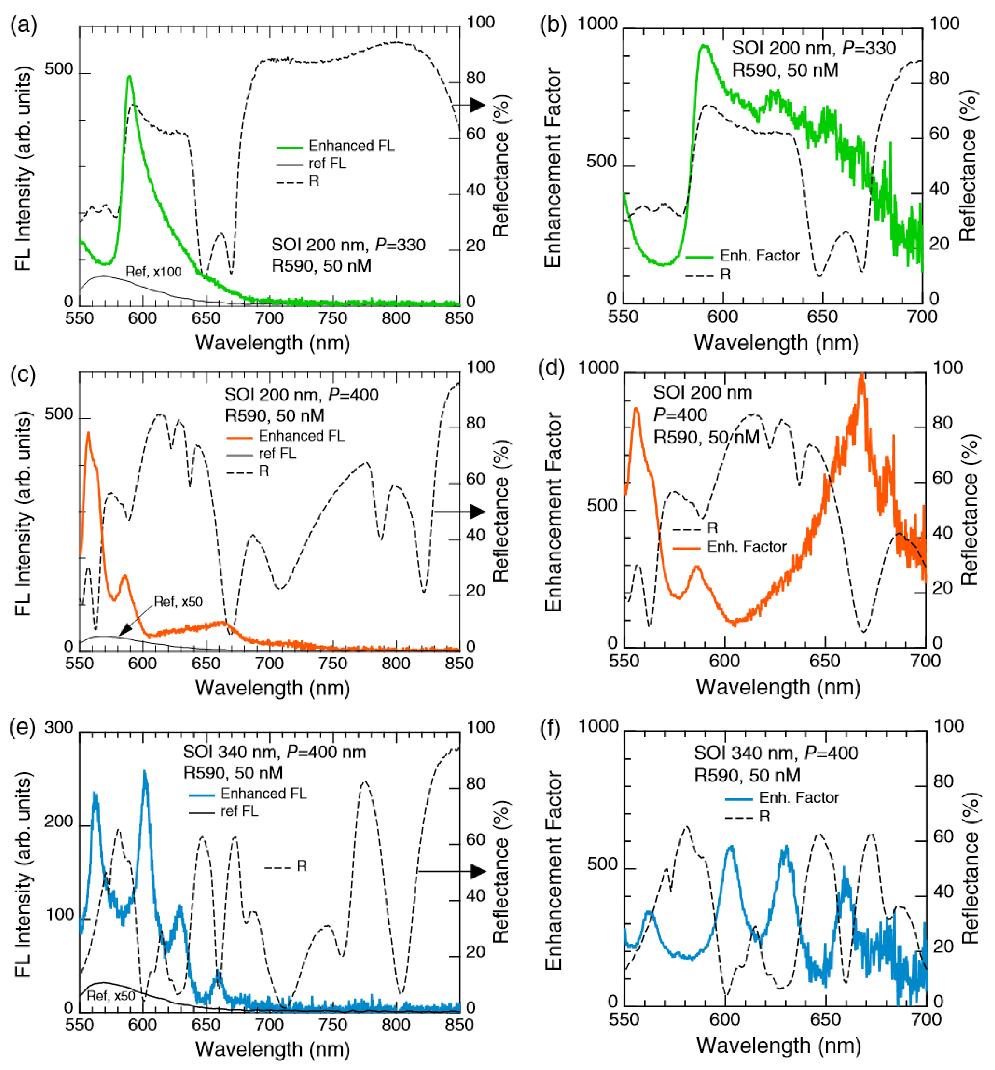
Figure 4.
(a) Numerically calculated R spectra for Si-rod-array metasurface of Si-rod height 200 nm and P = 330 nm. (b) Measured R spectra for the metasurface in Figure 2a,c. (c) Numerically calculated R spectra for Si-rod-array metasurface of Si-rod height 200 nm and P = 400 nm. (d) Measured R spectra for the metasurface in Figure 2b.

Figure 5.
(a) Numerically calculated R spectrum for the metasurface of a SOI of 200 nm thickness and P = 330 nm. Incidence was assumed to be normal. (b,c) xz-section-view |E| and |H| distributions, respectively, at a highly FL-enhancing wavelength (639.3 nm), indicated by the red arrow in (a). Incident |E| and |H| were set to 1.0.

Figure 6.
(a) Numerically calculated R spectrum for the metasurface of SOI thickness 200 nm and P = 400 nm. Incidence was assumed to be normal. (b,c) xz-section views of |E| and |H| distributions, respectively, at the wavelength (701.1 nm), indicated by the arrow with the label b,c in (a). (d,e) |E| and |H| distributions, respectively, at the wavelength (576.3 nm), indicated by the arrow with the label d,e in (a). Incident |E| and |H| were set to 1.0.
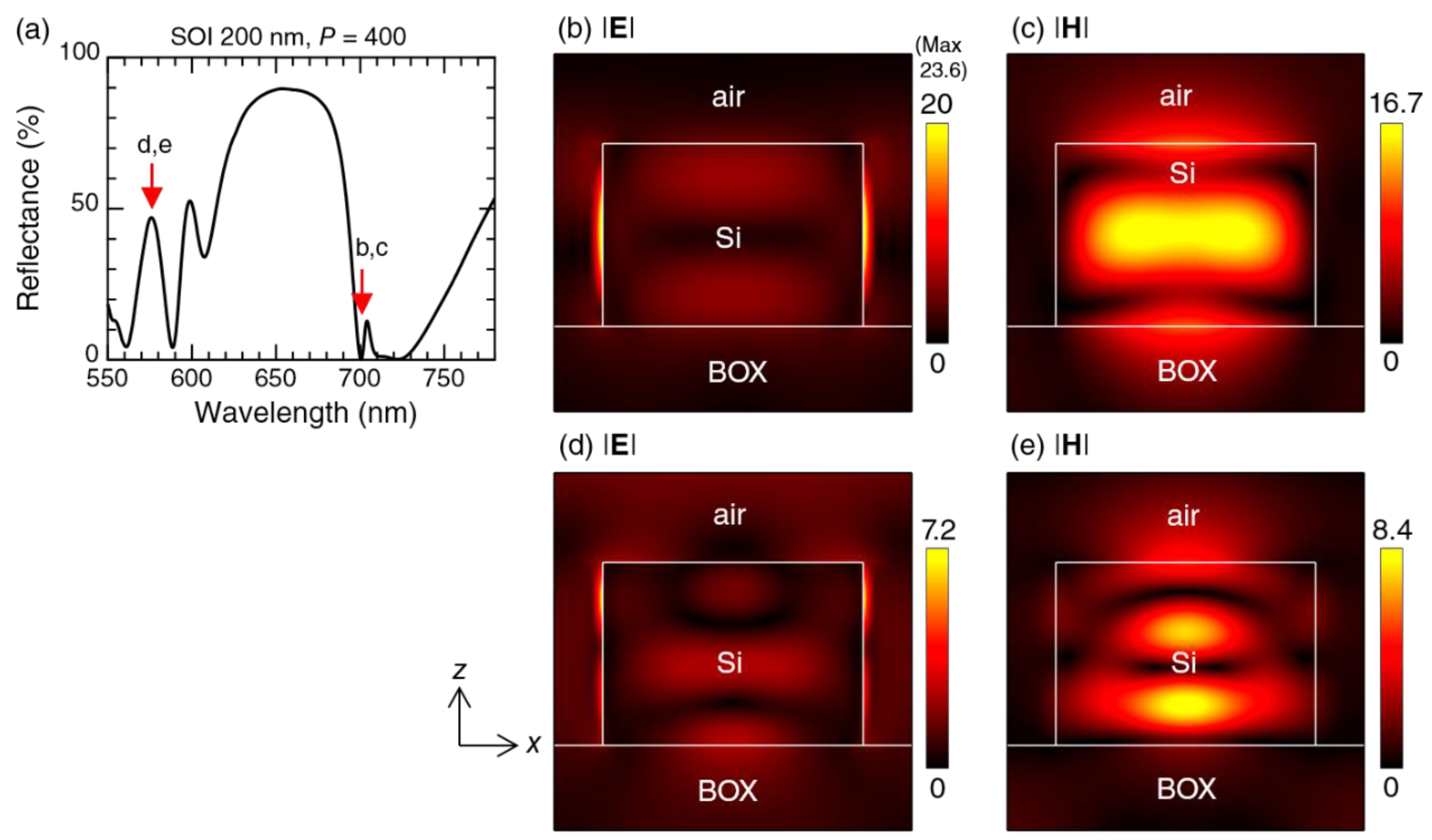
Figure 7.
(a) Numerically calculated R spectrum for the metasurface of SOI-thickness 200 nm and P = 340 nm. Incidence was assumed to be normal. (b,c) xz-section views of |E| and |H| distributions, respectively, at the wavelength (651.0 nm), indicated by the arrow with the label b,c in (a). (d,e) |E| and |H| distributions, respectively, at the wavelength (616.1 nm), indicated by the arrow with the label d,e in (a). Incident |E| and |H| were set to 1.0.
© 2018 by the author. Licensee MDPI, Basel, Switzerland. This article is an open access article distributed under the terms and conditions of the Creative Commons Attribution (CC BY) license (http://creativecommons.org/licenses/by/4.0/).
Share and Cite
MDPI and ACS Style
Iwanaga, M. All-Dielectric Metasurfaces with High-Fluorescence-Enhancing Capability. Appl. Sci. 2018, 8, 1328. https://doi.org/10.3390/app8081328
AMA Style
Iwanaga M. All-Dielectric Metasurfaces with High-Fluorescence-Enhancing Capability. Applied Sciences. 2018; 8(8):1328. https://doi.org/10.3390/app8081328
Chicago/Turabian StyleIwanaga, Masanobu. 2018. "All-Dielectric Metasurfaces with High-Fluorescence-Enhancing Capability" Applied Sciences 8, no. 8: 1328. https://doi.org/10.3390/app8081328
Note that from the first issue of 2016, this journal uses article numbers instead of page numbers. See further details here.