Complementary Cooperation of Dual Power Circuits to Drive Active Magnetic Bearings

Abstract
:
1. Introduction
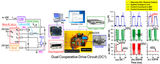
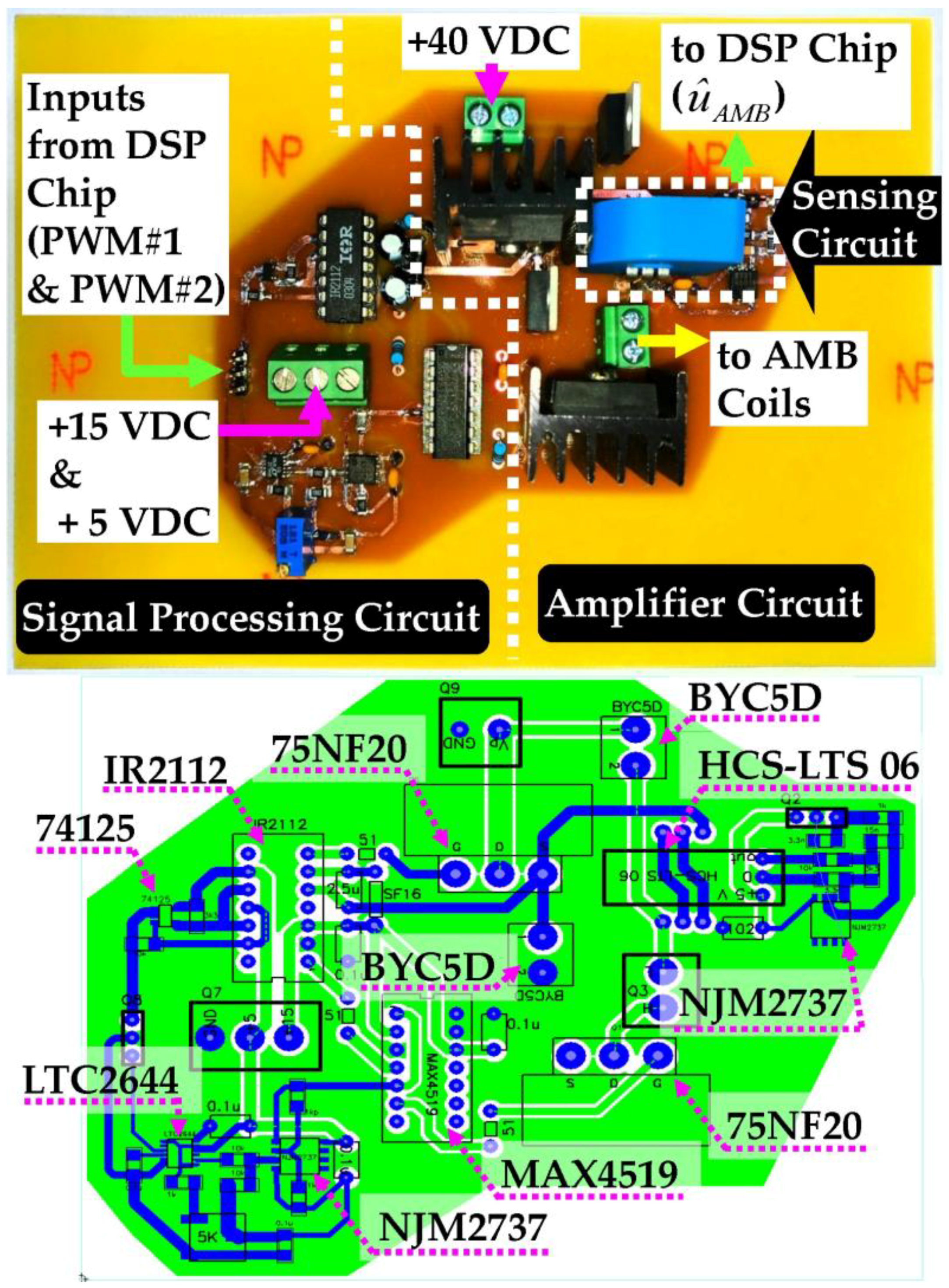
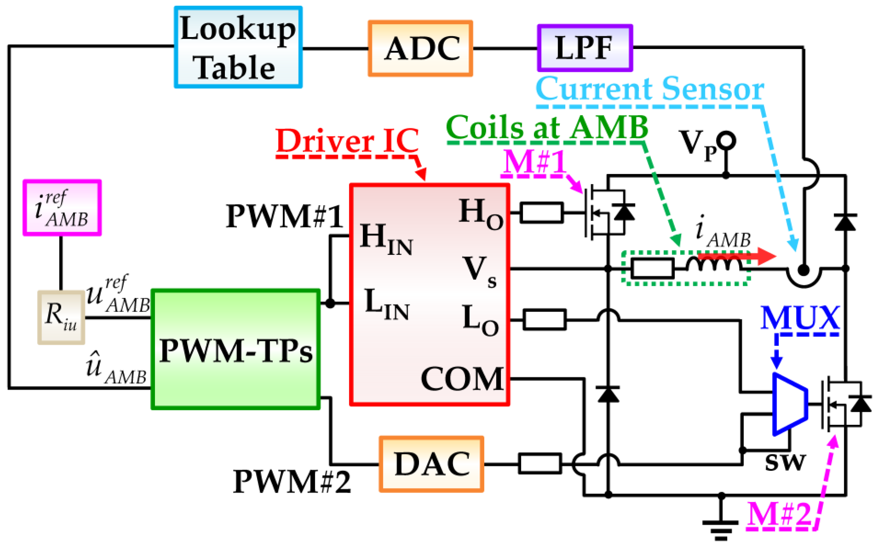
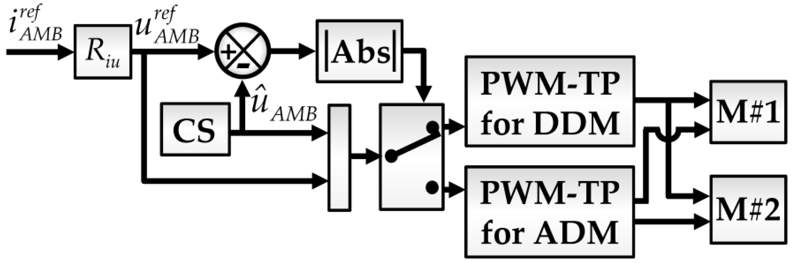
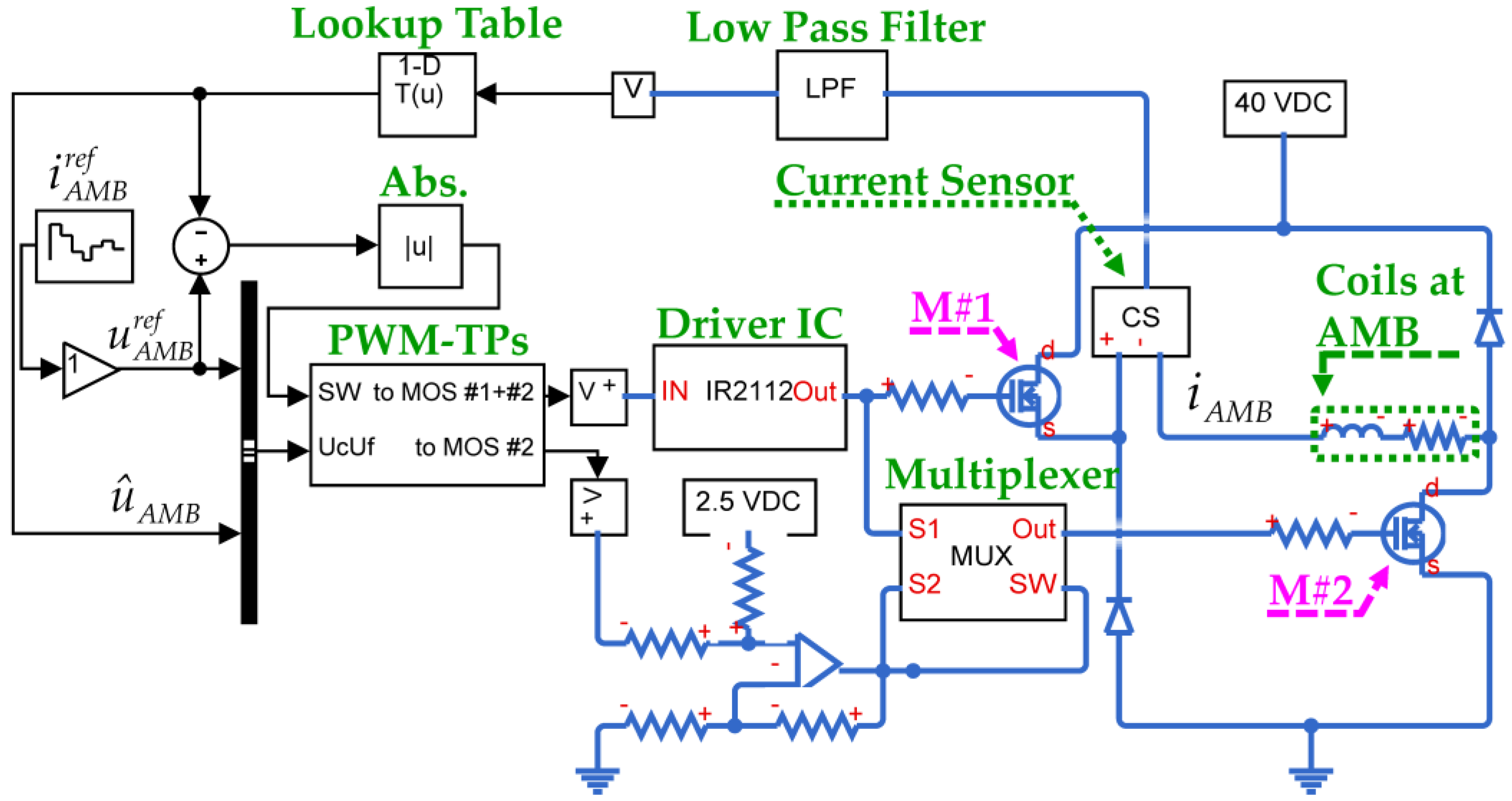
2. Design of Dual Cooperative Drive Circuit (DC2)
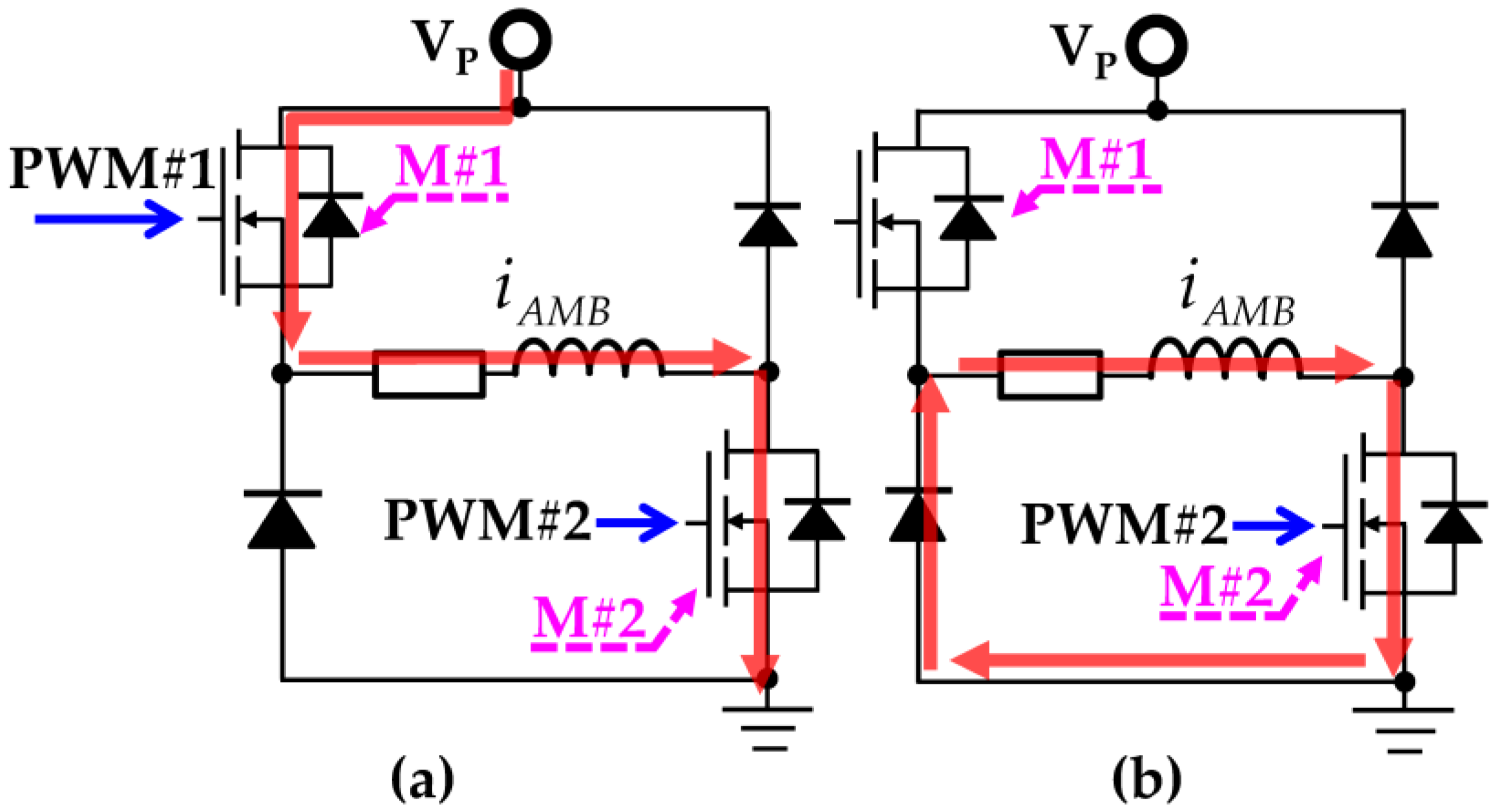
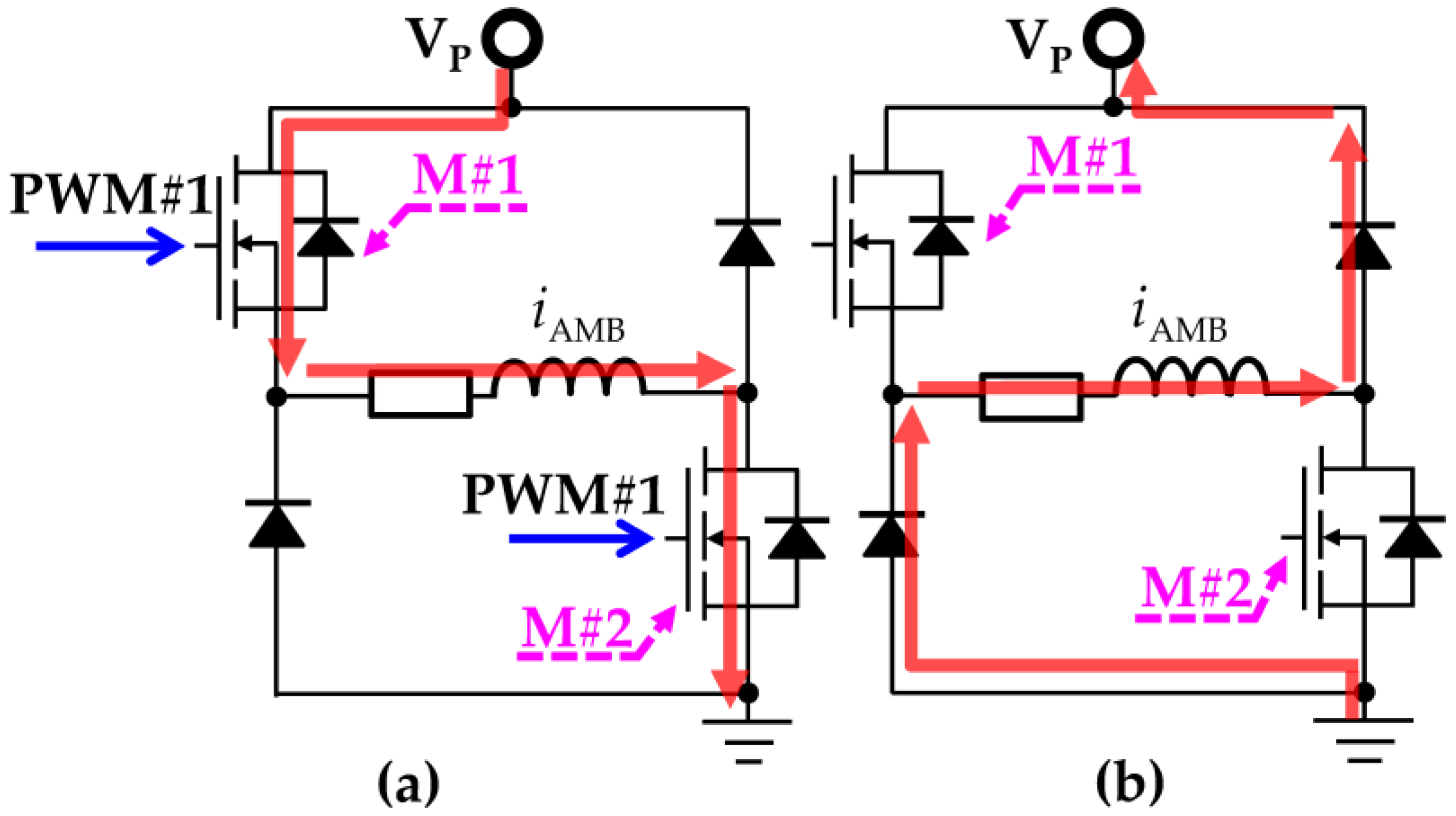
2.1. Digital Drive Mode (DDM)
2.2. Analog Drive Mode (ADM)
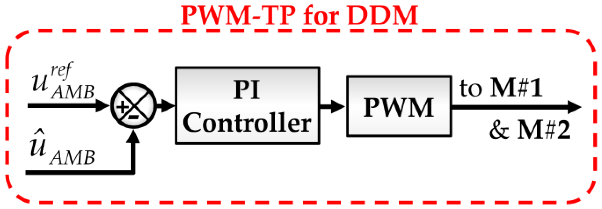
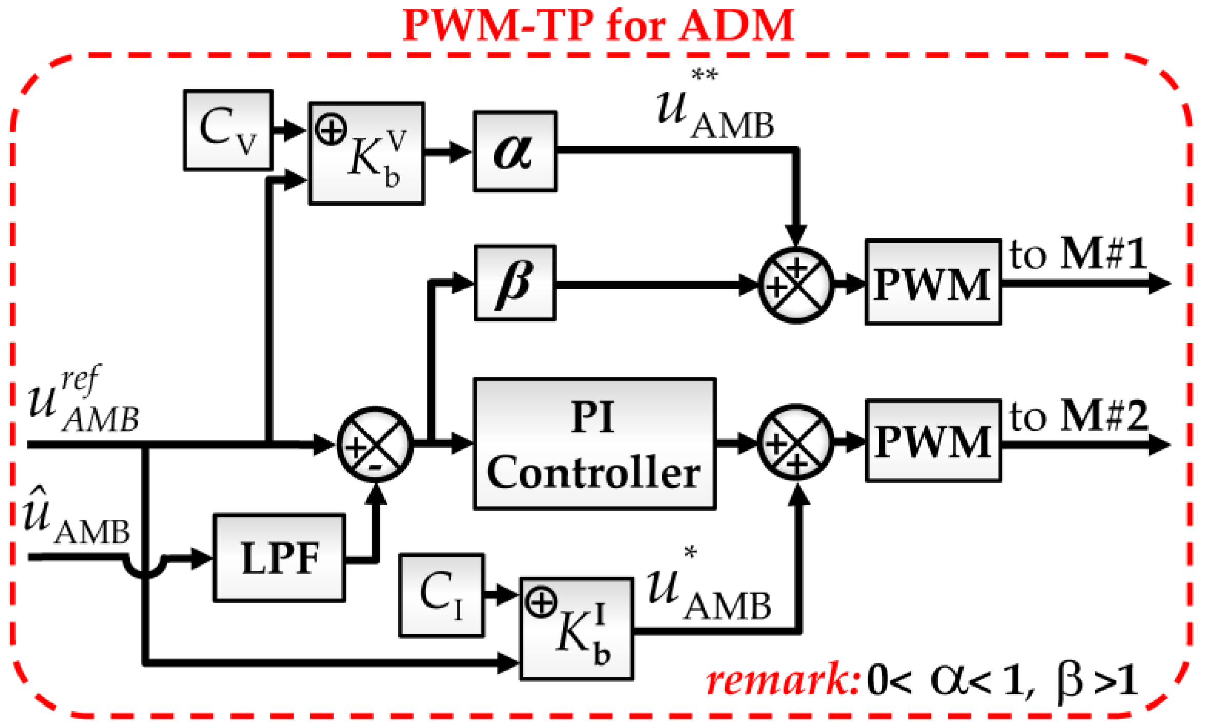
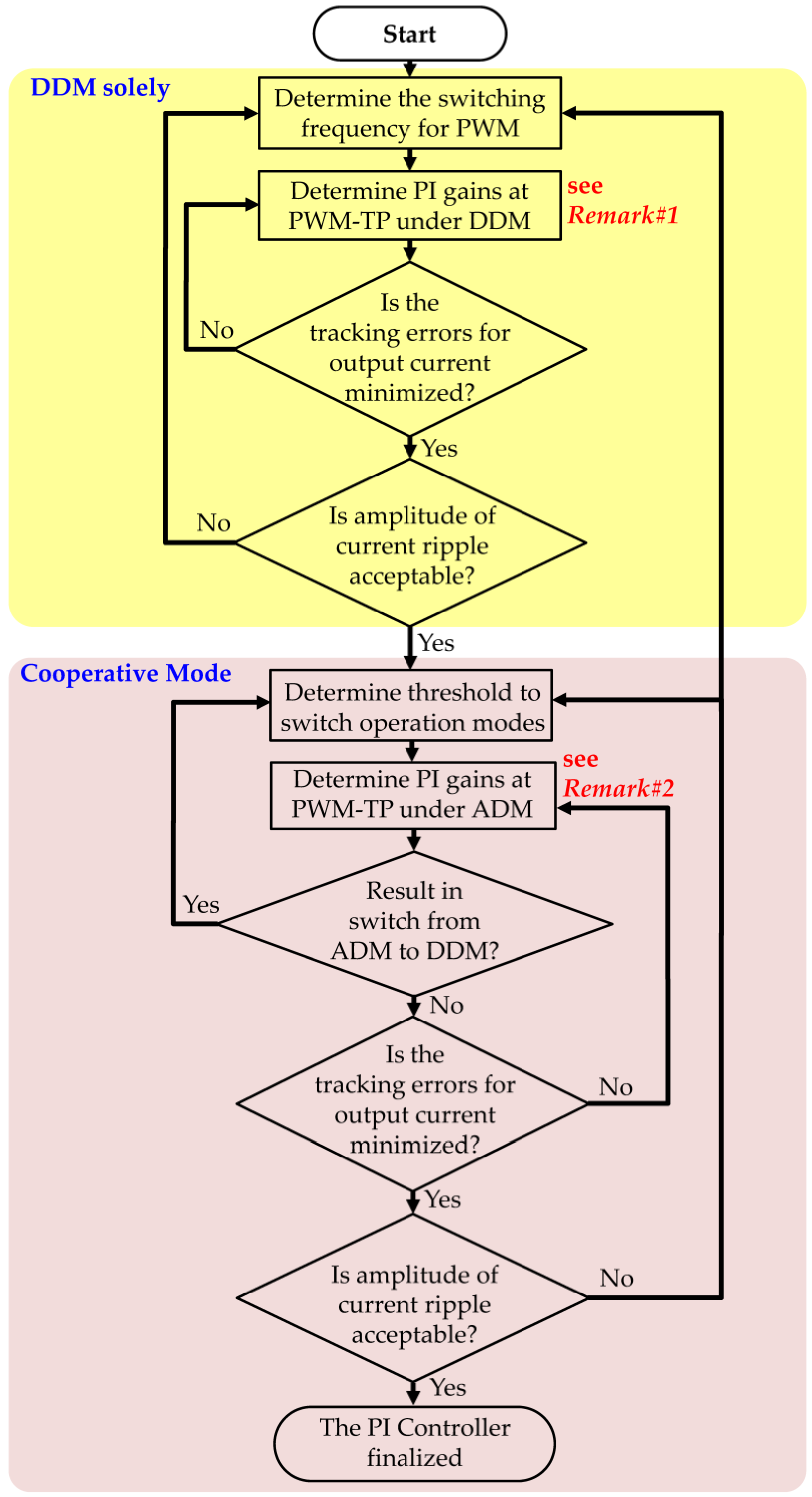
3. Pulse Width Modulation-Tuning Processors (PWM-TPs)
- Step 1
- Based on the step-wise reference shown in Section 4, the gain, , with respect to proportional action at PI controller is tuned from zero to infinity.
- Step 2
- As is tuned from zero to , the steady-state errors are all decreased gradually. By contrast, as is tuned from to infinity, the corresponding steady-state errors are all increased gradually.
- Step 3
- It is concluded that is the gain finally chosen.
- Step 4
- Secondly, the gain, , with respect to the integral action at PI controller is tuned from zero to infinity.
- Step 5
- It is observed that the steady-state errors are altered from negative values to positive values as from zero to infinity while is fixed. Therefore, is chosen since the corresponding steady-state errors are approximated to zero.
- Step 1
- Based on the step-wise reference shown in Section 4, the gain, , with respect to proportional action at PI controller is tuned from zero to infinity.
- Step 2
- As is tuned from zero to , the steady-state errors are all decreased gradually. By contrast, as is tuned from to infinity, the corresponding steady-state errors are all increased gradually.
- Step 3
- Different from the DDM, as , the tracking errors of output current would be more than the threshold such that ADM is cut off and then switched to DDM. In this case, we finally choose to prevent any potential switch to DDM.
- Step 4
- Secondly, the gain, , with respect to the integral action at PI controller is tuned from zero to infinity.
- Step 5
- It is observed that the steady-state errors are altered from negative values to positive values as from zero to infinity while is fixed. Therefore, is chosen since the corresponding steady-state errors are approximated to zero.
3.1. PWM-TP for DDM
3.2. PWM-TP for ADM
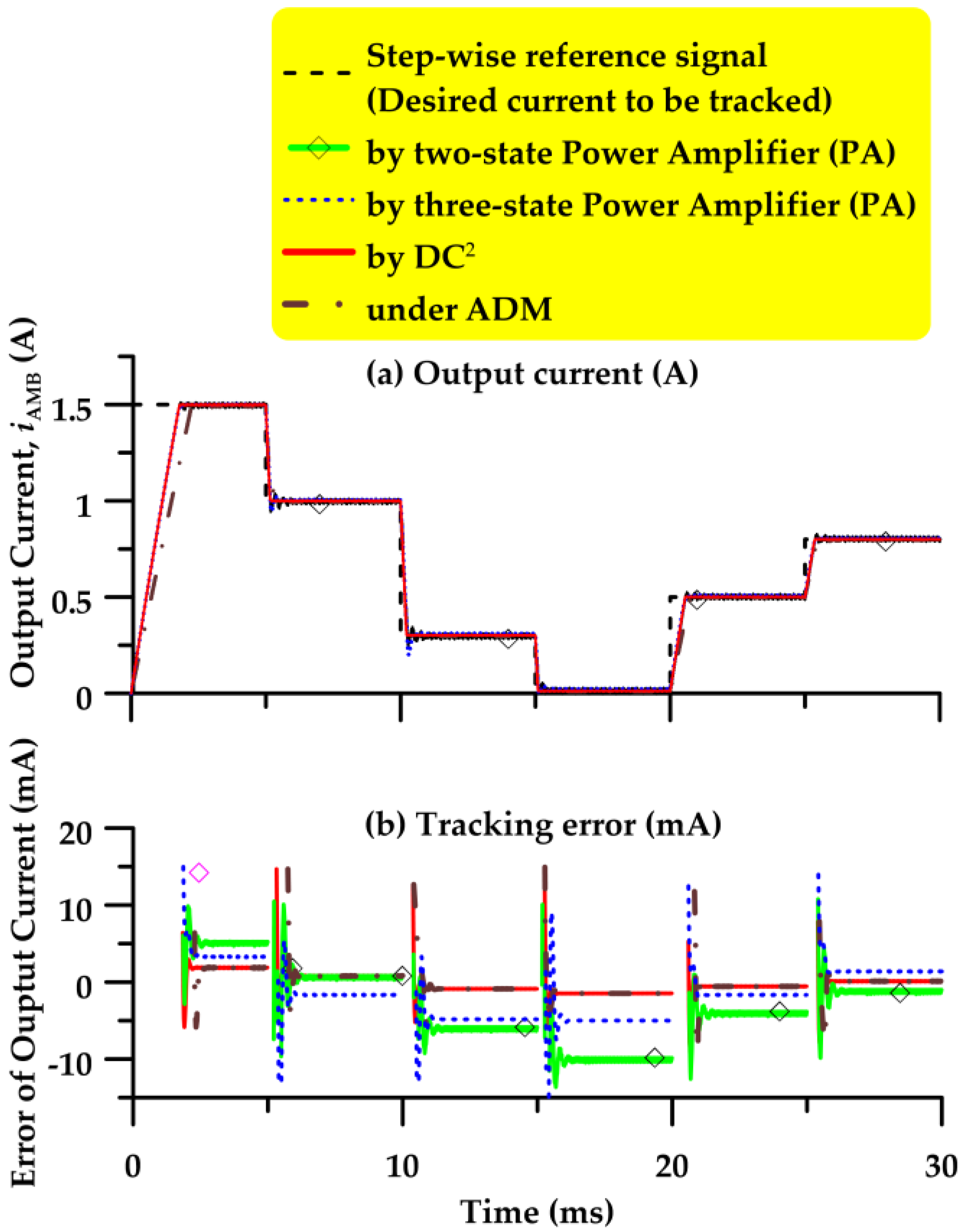
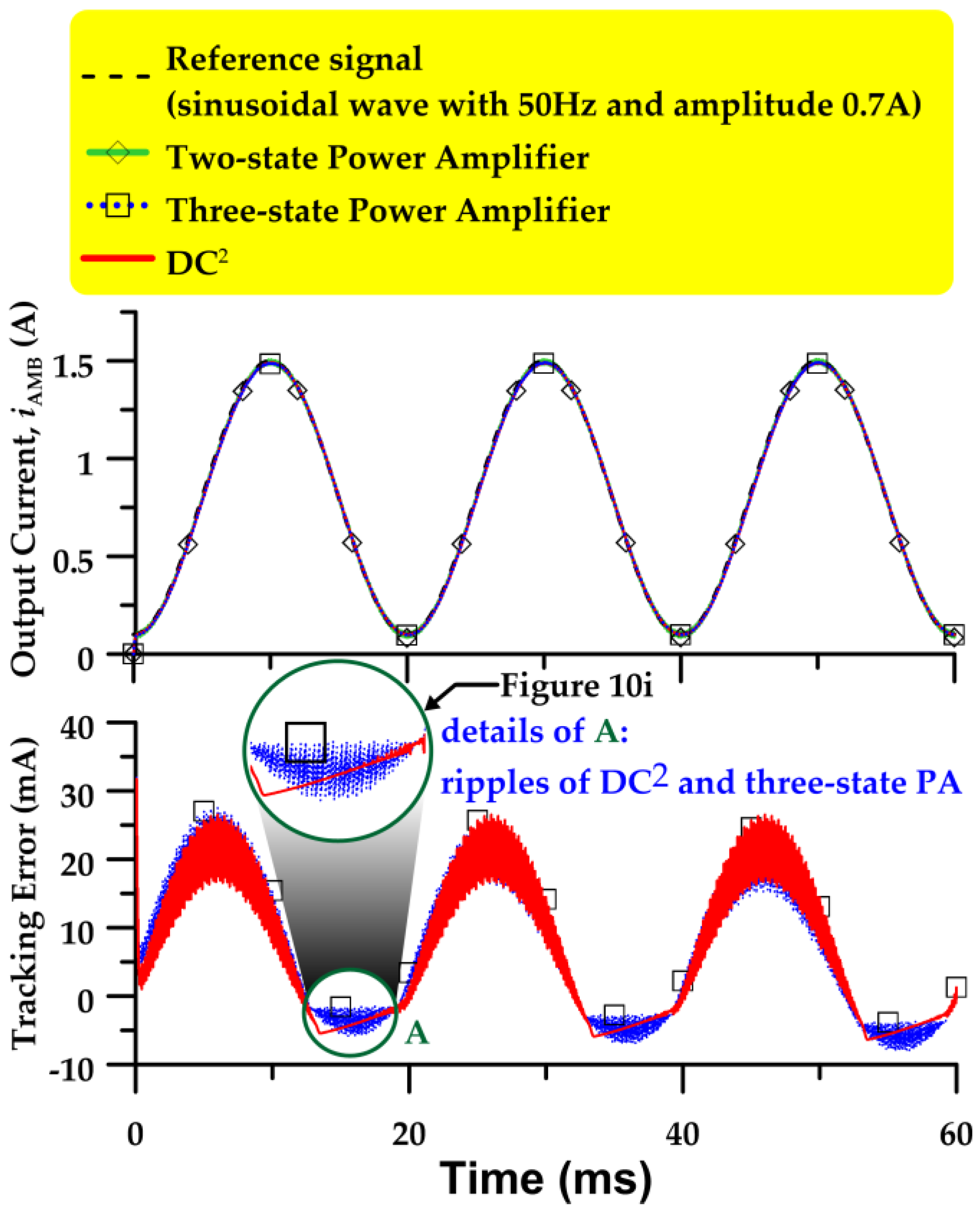
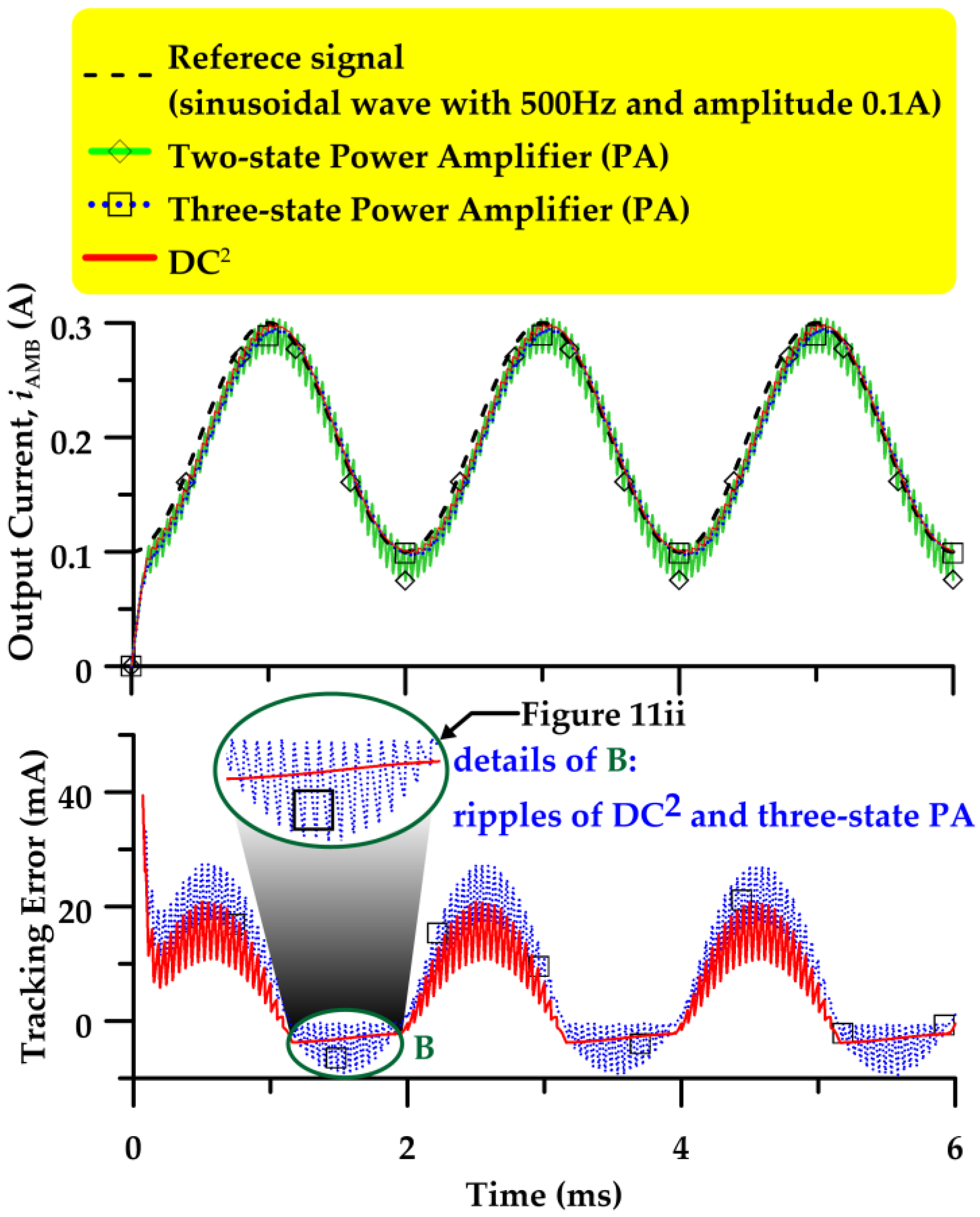
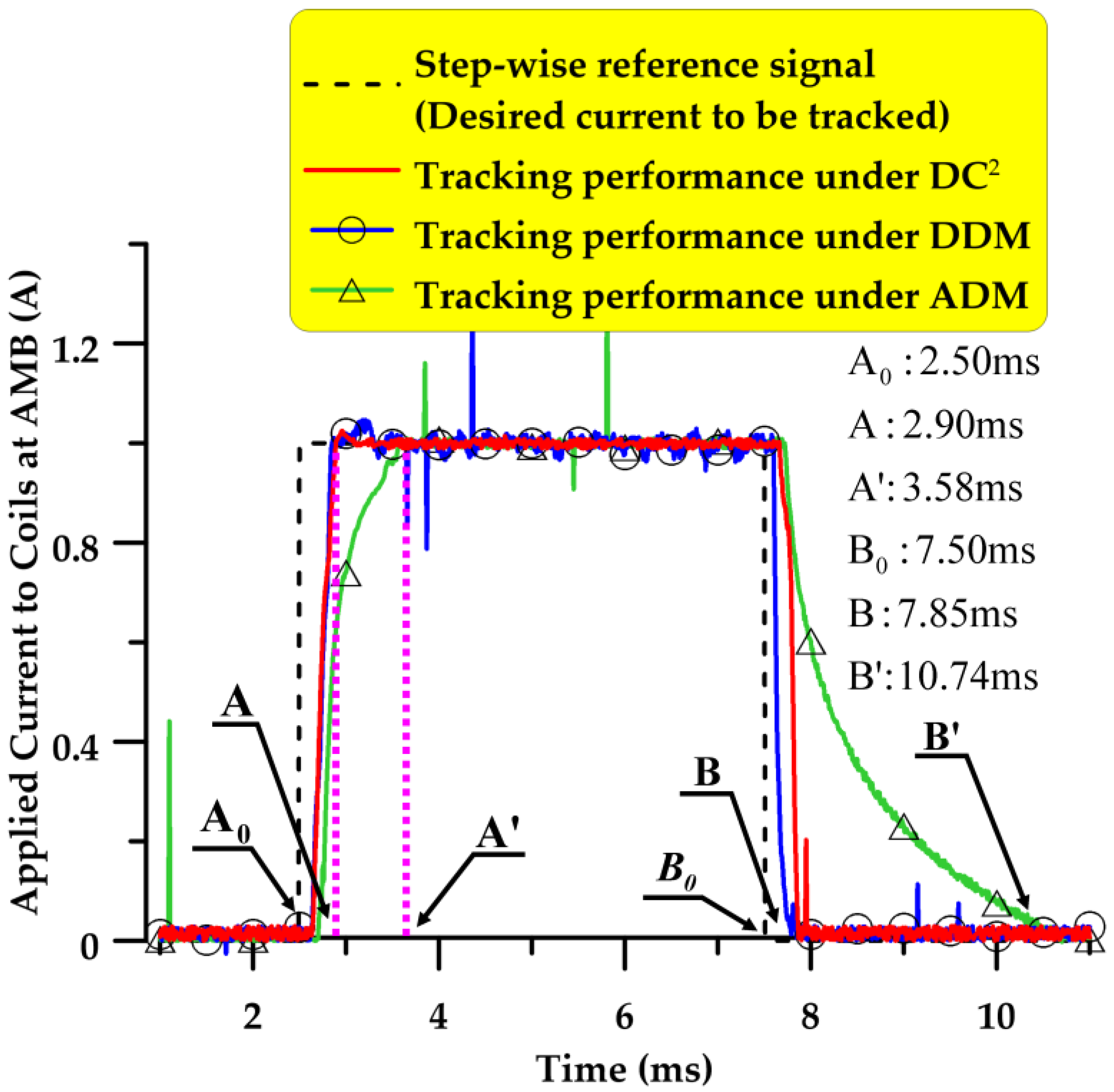
4. Simulations
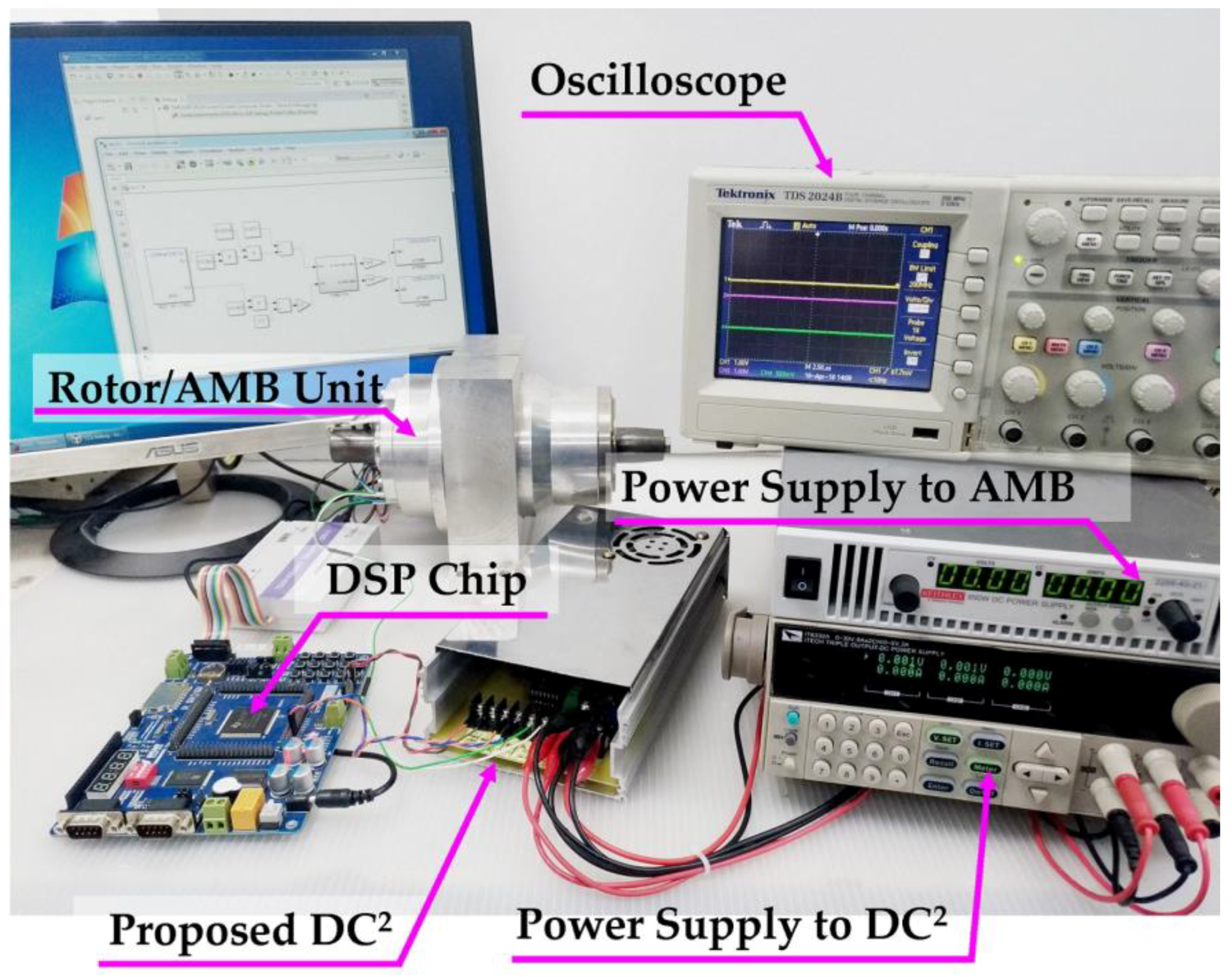
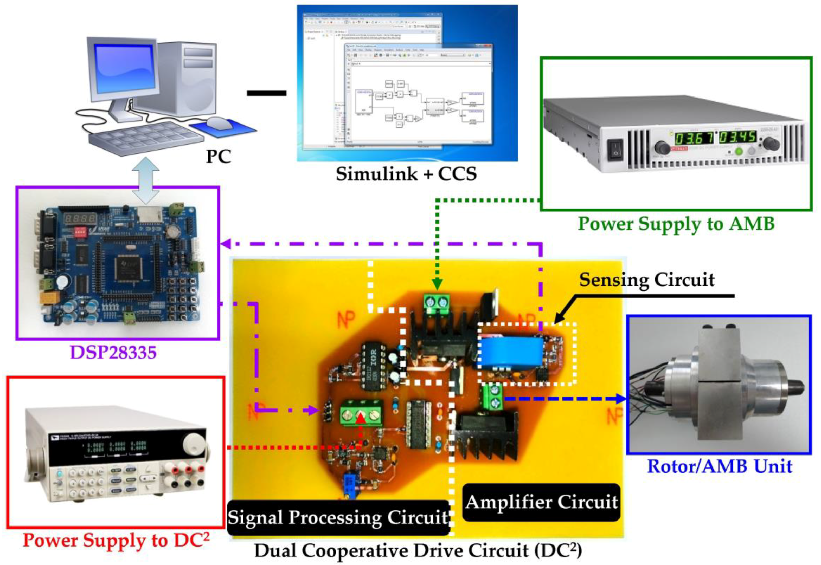
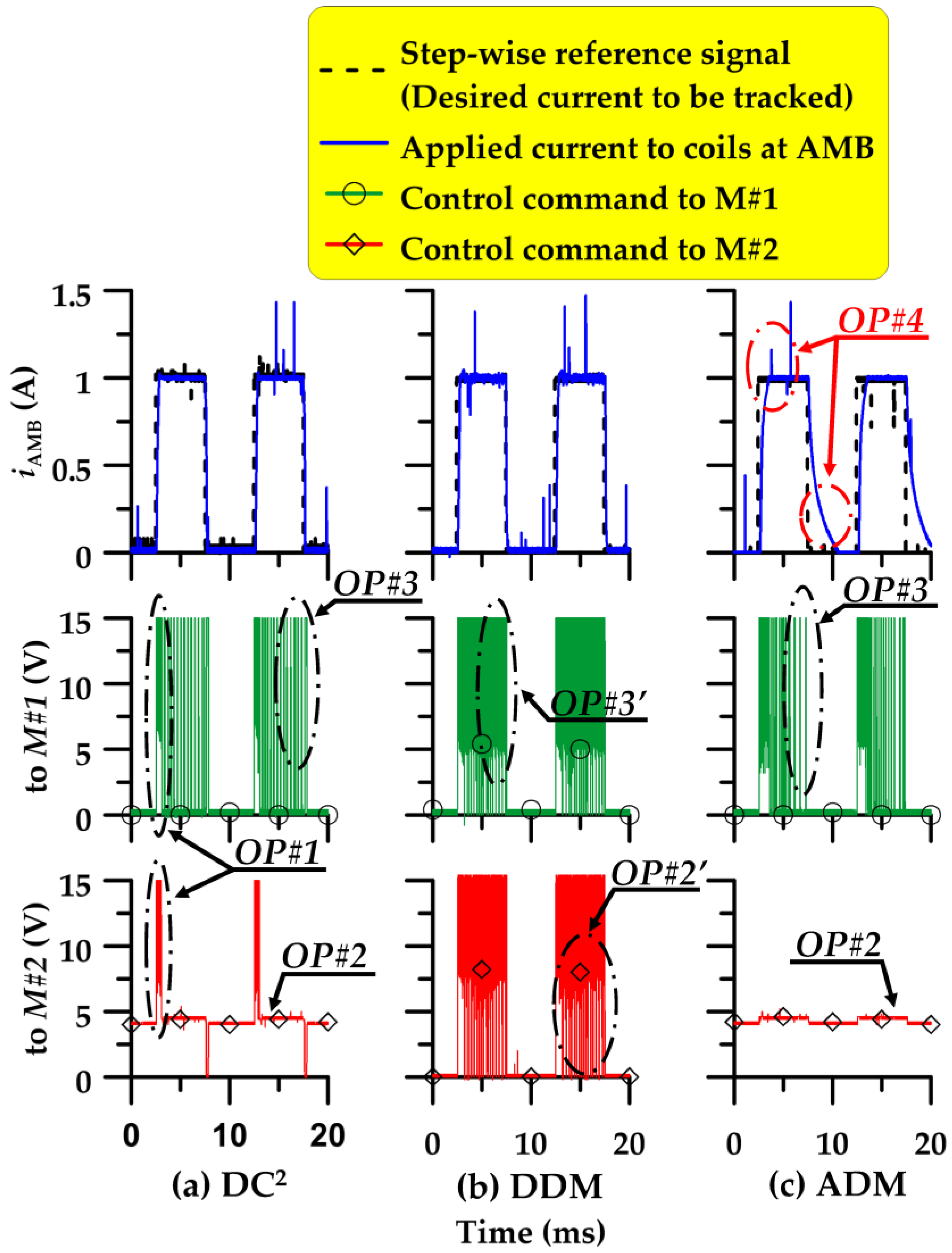
5. Experiments
6. Conclusions
Author Contributions
Funding
Acknowledgments
Conflicts of Interest
List of Abbreviations
| ADM | Analog Driving Mode |
| AMB | Active Magnetic Bearing |
| CS | Current Sensor |
| DAC | Digital to Analog Converter |
| DC | Direct Current |
| DC2 | Dual Cooperative Drive Circuit |
| DDM | Digital Driving Mode |
| DSP | Digital Signal Processor |
| EMI | Electromagnetic Interference |
| Imp. | Improvement |
| IC | Integrated Circuit |
| LPF | Low Pass Filter |
| MUX | Multiplexer |
| MOSFET | Metal-Oxide-Semiconductor Field-Effect Transistor |
| OP | Observation Point |
| PA | Power Amplifier |
| PD | Power Dissipation |
| PI | Proportional–Integral |
| PID | Proportional–Integral–Derivative |
| PPACR | Peak-to-Peak Amplitude of Current Ripple |
| PWM | Pulse Width Modulation |
| PWM-TP | Pulse Width Modulation-Tuning Processor |
| SLH | Switch-Linear Hybrid |
| TE | Tracking Error |
References
- Carabelli, S.; Muzzarelli, M. High-efficiency linear power amplifier for active magnetic bearings. IEEE Trans. Ind. Electron. 2000, 47, 17–24. [Google Scholar] [CrossRef]
- Cerruti, F.; Delprete, C.; Genta, G.; Carabelli, S. High efficiency and low cost power amplifiers and transducers for active magnetic bearings. In Proceedings of the Fourth International Symposium on Magnetic Bearings, Zurich, Switzerland, 23–26 August 1994. [Google Scholar]
- Ren, Y.; Fang, J. Current-sensing resistor design to include current derivative in pwm h-bridge unipolar switching power amplifiers for magnetic bearings. IEEE Trans. Ind. Electron. 2012, 59, 4590–4600. [Google Scholar] [CrossRef]
- Schulz, A.; Wassermann, J.; Schneeberger, M. A reliable switching amplifier for active magnetic bearings. In Proceedings of the IEEE International Conference on Industrial Technology, Maribor, Slovenia, 10–12 December 2003. [Google Scholar]
- Cao, G.; Lee, C.W. Development of PWM power amplifier for active magnetic bearings. In Proceedings of the Fifth World Congress on Intelligent Control and Automation, Hangzhou, China, 15–19 June 2004. [Google Scholar]
- Yoshida, T.; Kuroba, Y.; Ohniwa, K.; Osamu, M. Self-sensing active magnetic bearings using a new PWM amplifier equipped with a bias voltage source. Eur. Power Electron. Drives 2005, 15, 19–24. [Google Scholar] [CrossRef]
- Zhu, C.; Mao, Z. A PWM based switching power amplifier for active magnetic bearings. In Proceedings of the Eighth International Conference on Electrical Machines and Systems, Nanjing, China, 27–29 September 2005. [Google Scholar]
- Zhang, J.; Karrer, N. IGBT power amplifiers for active magnetic bearings of high speed milling spindles. In Proceedings of the 21st International Conference on Industrial Electronics, Control, and Instrumentation, Orlando, FL, USA, 6–10 November 1995. [Google Scholar]
- Wang, J.; Wang, L.; Dong, J.; Juang, C. Research on the steady state and ripple current models of current mode switching power amplifier for magnetic bearing. J. Softw. Eng. 2015, 9, 157–168. [Google Scholar] [CrossRef]
- Kashiwagi, S. A high-efficiency audio power amplifier using a self-oscillating switching regulator. IEEE Trans. Ind. Appl. 1985, IA-21, 906–911. [Google Scholar] [CrossRef]
- Jin, Q.; Ruan, X.; Ren, X.; Xi, H. High-efficiency switch-linear-hybrid envelope-tracking power supply with step-wave approach. IEEE Trans. Ind. Electron. 2015, 62, 5411–5421. [Google Scholar] [CrossRef]
- Jin, Q.; Ruan, X.; Ren, X.; Wang, Y.; Leng, Y.; Tse, C.K. Series-parallel-form switch-linear hybrid envelope-tracking power supply to achieve high efficiency. IEEE Trans. Ind. Electron. 2017, 64, 244–252. [Google Scholar] [CrossRef]
- Wang, Y.; Jin, Q.; Ruan, X. Optimized design of the multilevel converter in series-form switch-linear hybrid envelope-tracking power supply. IEEE Trans. Ind. Electron. 2016, 63, 5451–5460. [Google Scholar] [CrossRef]
- Silva, G.S.; Beltrame, R.C.; Schuch, L.; Rech, C. Hybrid AC power source based on modular multilevel converter and linear amplifier. IEEE Trans. Power Electron. 2015, 30, 216–226. [Google Scholar] [CrossRef]
- Tsai, N.C.; Kuo, C.H.; Lee, R.M. Regulation on radial position deviation for vertical AMB systems. Mech. Syst. Signal Process. 2007, 21, 2777–2793. [Google Scholar] [CrossRef]
- Tsai, N.C.; Chiang, C.W.; Li, H.Y. Innovative active magnetic bearing design to reduce cost and energy consumption. Electromagnetic 2009, 29, 406–420. [Google Scholar] [CrossRef]
- Tsai, N.C.; Lee, R.M. Regulation of spindle position by magnetic actuator array. Int. J. Adv. Manuf. Technol. 2011, 53, 93–104. [Google Scholar] [CrossRef]
- Tracxler, A.; Malsen, E. Hardware Components. In Magnetic Bearings: Theory, Design, and Application to Rotating Machinery, 1st ed.; Schweitzer, G., Maslen, E.H., Eds.; Springer: London, UK; New York, NY, USA, 2009; p. 98. ISBN 978-3-642-00496-4. [Google Scholar]
- MAXIM Integrated Products. Reliability Report for MAX4518ESD+; MAXIM Integrated Products: San Jose, CA, USA, 2010. [Google Scholar]
- Linear Technology. Reliability Data Report: Product Family R461; Linear Technology: Milpitas, CA, USA, 2015. [Google Scholar]


| Parameters | Value |
|---|---|
| Solver Type | Variable-step |
| Numerical Method | ode23t |
| Supply Voltage to AMB | 40 VDC |
| PWM Switching Frequency | 22 kHz |
| Threshold to Switch Operation Mode | 0.03 V |
| Threshold of Multiplexer | 3.005 V |
| Gate-source threshold voltage of MOSFET | 3 V |
| Drain-source on Resistance of MOSFET | 0.028 |
| Channel Modulation of MOSFET | 0.01 |
| Gate-source voltage for R_DS (on) | 10 V |
| Drain current for R_DS (on) | 75 A |
| Transresistance of Current Sensor | 1 |
| P Gain of PWM-TP under DDM | 300 |
| I Gain of PWM-TP under DDM | 1000 |
| P Gain of PWM-TP under ADM | 90 |
| I Gain of PWM-TP under ADM | 300 |
| Resistance of AMB coil | 0.9 |
| Inductance of AMB coil | 13 mH |
| A: Amplitude of | Two-State PA (DDM) | Three-State PA | DC2 | |||
|---|---|---|---|---|---|---|
| B: TE (mA) | C: Error C = B/A (%) | D: TE (mA) | E: Error E = D/A (%) | F: TE (mA) | G: Error G = F/A (%) | |
| 0.01 | 13.36 | 133.600 | 5.49 | 54.900 | 1.46 | 14.600 |
| 0.30 | 6.78 | 2.260 | 5.43 | 1.810 | 0.87 | 0.290 |
| 0.50 | 3.77 | 0.754 | 2.36 | 0.472 | 0.56 | 0.112 |
| 0.80 | 1.72 | 0.215 | 5.36 | 0.670 | 0.11 | 0.014 |
| 1.00 | 0.30 | 0.030 | 1.41 | 0.140 | 0.79 | 0.079 |
| 1.50 | 5.21 | 0.347 | 3.29 | 0.219 | 1.86 | 0.124 |
| Amplitude of | Two-State PA (DDM) | Three-State PA | DC2 | ||
|---|---|---|---|---|---|
| A: PPACR (mA) | D: PPACR (mA) | E: Imp. E = (A − D)/A | F: PPACR (mA) | F: Imp. F = (A − F)/A | |
| 0.01 | 31.4 | 2.4 | 92.36% | 1.7 | 94.59% |
| 0.30 | 30.5 | 4.6 | 84.92% | 3.4 | 88.85% |
| 0.50 | 30.0 | 5.5 | 81.67% | 4.2 | 86.00% |
| 0.80 | 29.3 | 5.8 | 80.20% | 5.2 | 82.25% |
| 1.00 | 28.9 | 6.3 | 78.20% | 5.8 | 79.93% |
| 1.50 | 27.7 | 7.5 | 72.92% | 7.2 | 74.01% |
| Amplitude of | Two-State PA (DDM) | Three-State PA | DC2 | ||
|---|---|---|---|---|---|
| A: PD (mW) | B: PD (mW) | C: Imp. C = (A − B)/A | D: PD (mW) | E: Imp. E = (A − D)/A | |
| 0.01 | 0.02 | <0.01 | 95.59% | <0.01 | 96.80% |
| 0.30 | 3.93 | 0.50 | 87.28% | 0.84 | 78.63% |
| 0.50 | 10.99 | 1.68 | 84.71% | 2.65 | 75.89% |
| 0.80 | 28.42 | 6.09 | 78.57% | 8.15 | 71.32% |
| 1.00 | 44.69 | 11.20 | 74.94% | 14.08 | 68.49% |
| 1.50 | 102.06 | 32.76 | 69.90% | 39.69 | 61.11% |
© 2018 by the authors. Licensee MDPI, Basel, Switzerland. This article is an open access article distributed under the terms and conditions of the Creative Commons Attribution (CC BY) license (http://creativecommons.org/licenses/by/4.0/).
Share and Cite
Chiu, H.-L.; Tsai, N.-C. Complementary Cooperation of Dual Power Circuits to Drive Active Magnetic Bearings. Appl. Sci. 2018, 8, 1270. https://doi.org/10.3390/app8081270
Chiu H-L, Tsai N-C. Complementary Cooperation of Dual Power Circuits to Drive Active Magnetic Bearings. Applied Sciences. 2018; 8(8):1270. https://doi.org/10.3390/app8081270
Chicago/Turabian StyleChiu, Hsin-Lin, and Nan-Chyuan Tsai. 2018. "Complementary Cooperation of Dual Power Circuits to Drive Active Magnetic Bearings" Applied Sciences 8, no. 8: 1270. https://doi.org/10.3390/app8081270
APA StyleChiu, H.-L., & Tsai, N.-C. (2018). Complementary Cooperation of Dual Power Circuits to Drive Active Magnetic Bearings. Applied Sciences, 8(8), 1270. https://doi.org/10.3390/app8081270