Biomimetic Surface Structuring Using Laser Based Interferometric Methods
by
Andrés Fabián Lasagni
1,2,*, 
Sabri Alamri
2, 
Alfredo Ismael Aguilar-Morales
2,
Florian Rößler
1,
Bogdan Voisiat
1 and
Tim Kunze
2 1
Institute for Manufacturing Technology, Technische Universität Dresden, 01069 Dresden, Germany
2
Fraunhofer-Institut für Werkstoff- und Strahltechnik IWS, Winterbergstr. 28, 01277 Dresden, Germany
*
Author to whom correspondence should be addressed.
Appl. Sci. 2018, 8(8), 1260; https://doi.org/10.3390/app8081260
Submission received: 13 July 2018
/
Revised: 23 July 2018
/
Accepted: 25 July 2018
/
Published: 31 July 2018
(This article belongs to the Special Issue Biomimetic Laser Processing)
Abstract
:This review investigates the capabilities of laser-based interferometric methods for producing structures with multiple-scaled surface features imitating natural examples. Firstly, laser interference lithography is used to produce hierarchical patterns with length-scales in the micrometer and sub-micrometer range. Different strategies are discussed to produce a wide variety of periodic arrays, depending on the number of resist lasers used as well as the way in which the exposure steps are organized. After that, periodic patterns are fabricated on polymers using ns laser pulses from an UV-laser system. Additionally in this case, multiple-scale patterns are produced by using different strategies. A similar approach is described to treat metallic surfaces of steel X6Cr17 and a titanium alloy Ti6Al4V. The geometry of the produced microstructures was characterized using scanning electron microscopy and confocal microscopy. Measurement of water contact angle is performed for both polymer and metallic surfaces.
1. Introduction
Living organisms have evolved to well-adapted structures and materials over time through natural selection and evolution [1]. In particular, biomimetics has given rise to new technologies inspired by biological solutions at micro and nanoscales. In this scenario, nature provides a wide range of surfaces with specific functions and properties [2,3,4,5]. In consequence, the fabrication of structures in the micro- and nano-range can permit to design materials with advanced surface properties by tailoring desired material properties [6]. These complex designs are only possible to fabricate on industrial products using novel fabrication techniques, offering both high resolution and throughput.
Mimicking natural designs helps in understanding the related phenomena and correlate topographies with specific mechanisms and functions. One of the most studied surface functions is related to the control of the wettability of solids, which have attracted interest from both fundamental and practical perspectives [7]. The wettability is usually determined by measuring the contact angle (CA) of a water droplet on a solid surface. According to the most common definitions, a surface can be described as superhydrophobic, when its water contact angle (WCA) is higher than 150°. Some superhydrophobic surfaces can cause water and even oil to roll-off leaving little or no residue and simultaneously carry away surface contamination, showing self-cleaning properties [5,8,9]. The best known example of self-cleaning surface is the lotus leaf (Nelumbo nucifera) or the Colocasia esculenta, a symbol of purity for thousands of years [8]. In particular these leaves present a large diversity of hierarchical surface structures ranging from micro to the nanometer scale, which have been studied with the help of scanning electron microscopy techniques [8,9]. The Lotus-Effect is however not restricted to plants, but it can be also found on insects skin or wings [10,11].
Another important example in which functional microstructures play a fundamental role is the skin of the ventral body of snakes. Several studies have in fact revealed that their motion is facilitated since the surface of the snake skin generates low friction when sliding in the forward direction, and at the same time produces high friction along the substrate for pushing the body forward [12].
Thus, the term biomimetics, referred to the “imitation of life”, has become popular in the fields of science and engineering due to the endless potential technological ideas in large functional surfaces. The numerous surfaces observed on plants and animals can serve as the base of enhancement of technological functions [2].
Mimicking micro patterns can be achieved by different routes [7]. Many of them normally exhibit micro- or nanosized roughness as well as hierarchical structures. In the field of non-contact manufacturing process, laser-based methods have shown a considerable development for mimicking natural examples. For instance, direct laser writing method have been used to control the wettability of surfaces using nanosecond [13,14], picosecond [15] and femtosecond [16,17,18,19] laser sources.
In particular, Direct Laser Interference Patterning (DLIP) offers high flexibility and throughput for feature sizes in the micro- and nano-range [20,21,22,23]. The DLIP principle is based on the periodic modulation of the laser intensity which can be obtained by the generation of interference patterns between two or more coherent laser beams. The produced intensity distribution allows irradiating relative large areas using even only a single pulse. The geometry of the patterns can be transferred to metals, polymers or ceramics by different ablation processes. Furthermore, when utilizing fs-lasers, even very complex 3D patterns such nano-bumps and nano-wire arrays can be fabricated [24]. The periodicities as well as features sizes that can be obtained are a function of the number of used laser beams, their polarization, the individual angle of incidence and the laser intensity. The throughput rates of the DLIP technology allow today to fabricate homogeneous surface microstructures at low cost and even in a one-step process what is of high importance for real industrial processes [25].
In this review, DLIP is used for the fabrication of microstructures mimicking natural surfaces, in particular, when using ns and ps laser sources. The geometry of the produced microstructures was characterized using scanning electron microscopy and confocal microscopy. Different processing strategies are introduced to treat photoresist, dielectric polymers and metals.
2. Materials and Methods
2.1. Materials
The experiments detailed in this work were carried out on different polymers, metals and photoresist. Commercially available flat samples sheets of X6Cr17 corrosion resisting ferritic steel (type 1.4016) and Ti6Al4V were used, with thicknesses of 0.78 mm and 1.8 mm, respectively. After the laser treatment process, the samples were cleaned with ethanol in the ultrasonic bath during 60 min, to remove particles produced during the ablation.
Transparent commercial polycarbonate (PC) sheets (H&S Kunststofftechnik GmbH, Siegen, Germany) with a nominal thickness of 5 mm were also used. These substrates were used as received.
In the case of the photoresist materials, silicon substrates (purchased from Active Business Company GmbH, Brunnthal, Germany) were ultrasonically cleaned with acetone and isopropanol. Afterwards, the photoactive resist SU 8-2 (Microchem Corp., Westborough, MA, USA) was spin coated on the wafer at 3000 rpm for 60 s, obtaining a layer thicknesses of 2 µm (SU8-2).
2.2. Direct Laser Interference Patterning
Different two-beam interference setups were utilized to produce the different hierarchical geometries on all investigated materials. In the case of metals, the DLIP experiments were carried out using a IR (1064 nm) picosecond laser (solid-state Q-switched Innoslab Nd:YVO4, pulse duration 10 ps, repetition rate of 1 kHz) combined with a DLIP optical head (Fraunhofer IWS) which allow to split the main laser beam into two sub-beams which are later recombined by an aspherical lens on the materials surface producing the line-like pattern at the interference area.
For the polycarbonate material, a nanosecond UV (263 nm) laser system was used. In this case, a Q-switched diode-pumped solid-state laser (Laser Export, TECH-263 Advanced) was used, with a pulse duration of 3 ns, a repetition rate of 1 kHz and a maximal pulse energy of 50 µJ. The experiments were conducted also using a self-developed DLIP system (DLIP-µFAB, Fraunhofer IWS), producing pixels containing the line-like interference pattern with diameters of ~20 µm. Taking into consideration the optical loses, irradiances up to ~3.109 W/cm² can be reached. To cover larger areas, the substrate was translated in X and Y directions and a specific distance between the pixels were defined.
In the case of the resist materials, a standard DLIP beam splitter configuration was used [26]. Before irradiation, the samples were pre-baked on a hotplate at 95 °C for 2 min. Following, the substrate was exposed using an 8 ns pulsed Nd:YAG laser (Quanta Ray Pro 290-10) with the 3rd harmonic wavelength (355 nm) and a repetition rate of 10 Hz. The beam splitter set-up was used to overlap both beams with an angle of θ = 4.07° and θ = 41.59° to reach spatial periods of Λ = 5.0 µm and Λ = 0.5 µm, respectively. The samples were irradiated with two single pulses with a 60° rotation in between to obtain a hole-like pattern with a hexagonal arrangement. The laser fluence was set to 4 mJ/cm² and 7.5 mJ/cm² for fabricating 0.5 µm and 5 µm periodic patterns, respectively. After the exposure, the samples were post-baked at 95 °C for 2 min. The development of the SU-8 was carried out by dipping the samples into the mr-dev 600 (Microchem Corp.) developer solution for 1 min. Subsequently, the samples were rinsed in isopropanol in the same way for 1 min and were hard baked at 95 °C for 5 min.
2.3. Surface Characterization
The morphology of structured samples was characterized using confocal microscopy (Sensofar S Neox, Barcelona, Spain) employing a 150 × magnification objective with a nominal lateral resolution of 140 nm and vertical resolution of 2 nm. Structures with spatial periods smaller than 1 µm were also characterized using atomic force microscope (nanosurf core AFM). In the last case, a total area of 20 µm × 20 µm was measured. Measurements were performed in a dynamic measuring or amplitude mode (AM-AFM), where the cantilever oscillates on a high frequency in a certain distance close to the surface. The static water contact angle measurements (OCA 20, Dataphysics) were carried out using 2 µl of deionized water, in the environment of 23.3 °C and 40.0% relative humidity, fitting each droplet shape with the tangent searching method and repeating the measurement 4 times. The reference value for the water contact angle of the polycarbonate used in this work has been measured to 87.8° ± 0.4°.
3. Results and Discussion
3.1. Laser Interference Lithography Fabrication
Laser interference lithography was used to fabricate hexagonal arranged hole-like patterns in SU-8-2. These structures were achieved by irradiating a spin-coated layer of non-polymerized SU-8. To obtain the hole-like patters, two exposure steps were applied with a rotation of 60° between them. On the positions corresponding to the interference maxima, the SU-8 material starts to polymerize forming the periodic structure. By varying the laser fluence between 1–8 mJ/cm², the amount of polymerized material can be controlled and thus the diameter of the produced holes. In the case of small spatial periods, lower fluences are required to avoid the full polymerization of the SU-8 layer.
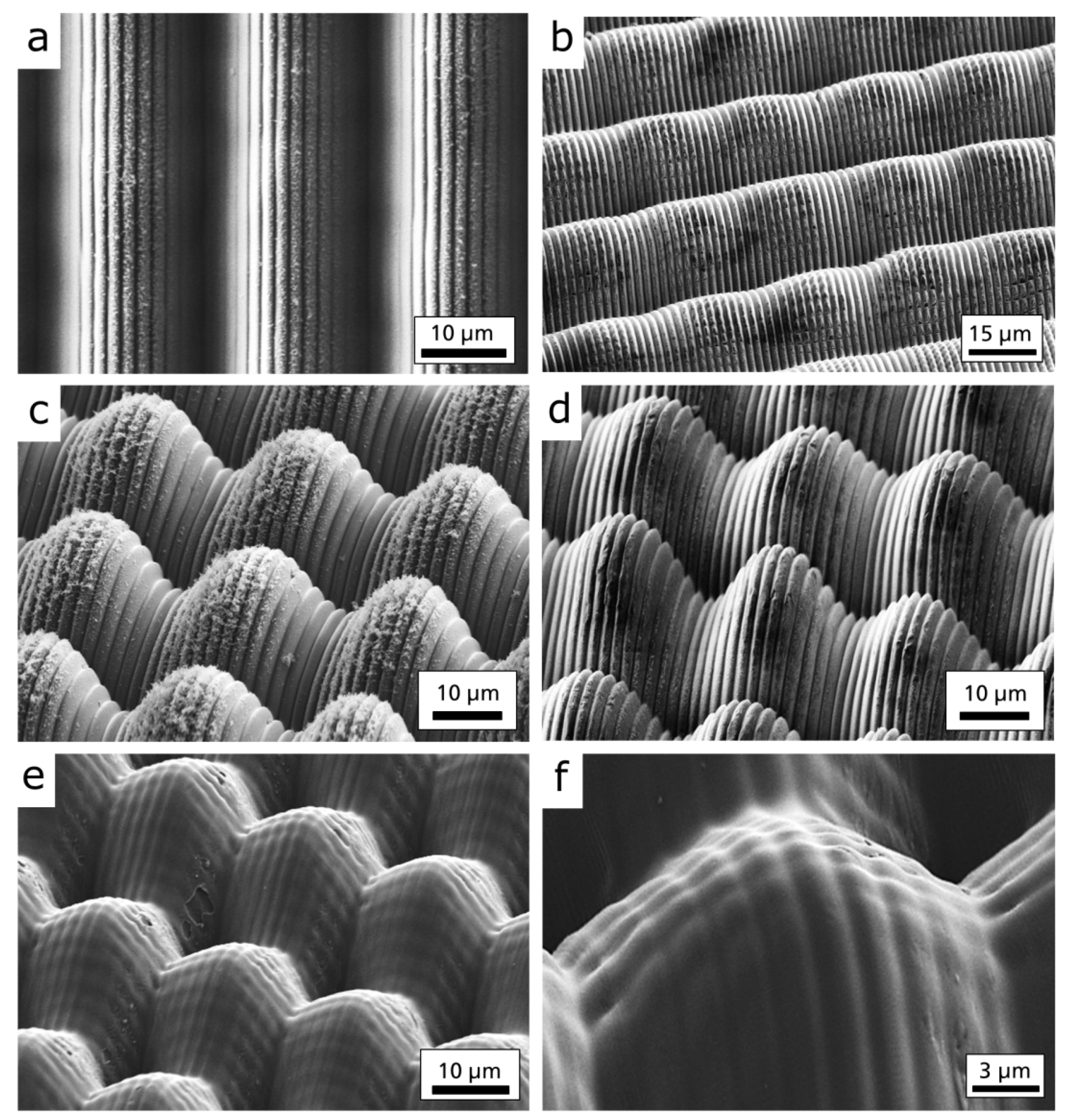
This first study permitted to determine the most adequate fluences for the fabrication of the biomimetic hierarchical surface structures. In this case, fluences of 7.5 mJ/cm² and 4 mJ/cm² for the 5 µm and 0.5 µm patterns were used, respectively. Scanning electron microscope images of resulting two-level hierarchical patterns fabricated using three different strategies are shown in Figure 1.
Figure 1a,b shows a hexagonal hole-like structure with a 0.5 µm spatial period covered with a 5.0 µm hole-like structure. This strategy for fabricating hierarchical structures has been developed before as reported in [27]. First, a single-scale pattern with 0.5 µm spatial period was applied on a silicon wafer as described in the experimental section. After the hard baking step, the patterned wafer was spin coated again and the exposure setup was changed to fabricate a 5 µm hole-like pattern. Finally, the wafer was baked, developed, rinsed and hard baked again to finish the second layer. It is visible in Figure 1a that the 5.0 µm hole-like pattern dominates the surface topography. Only within the holes of the large-scale structure, the small-scale structure is visible. In addition, since two layers of the resist were applied, the 0.5 µm geometry can be observed below the large pattern.
In Figure 1c, hierarchical patterns fabricated with a similar strategy are shown. In this case, the largest periodic pattern was fabricated first. Then, the pre-patterned substrate with the 5.0 µm structure was covered with a second layer of SU-8 which was later exposed to the interference patterns with the 0.5 µm spatial period geometry. As it can be seen in the image, the small-scale structure dominates the surface, since it covers the whole surface of the 5 µm pattern. The difference to a single-scale pattern is that the 0.5 µm pattern topography is now modulated with the 5 µm topography lying underneath. Consequently, the small-scale pattern is on different height levels at different lateral positions.
Finally, a second strategy for the production of multi-scale patterns was used. Here, a single layer of SU-8 was exposed first with the 5 µm spatial period setup and later with the 0.5 µm spatial period setup. Between the irradiation steps any other treatment was performed. As it can be seen in Figure 1d, the small-scale structure of 0.5 µm spatial period is visible mainly at the regions corresponding to the interference minima positions of the larger 5.0 µm pattern. It is also evident from the image that both geometries are at the same level, since only one layer of the resist was applied. Compared to the previous described strategy, the small-scale structures dominates in this case, probably because the laser exposure dose which corresponds to the large patterns was not high enough to totally polymerized the used SU-8 layer.
In addition to SEM images, the surface topography of the fabricated patterns was characterized using AFM. The results are shown in Figure 2. From Figure 2a,b, the structure height of the 5 µm on 0.5 µm hierarchical patterns using the first strategy can be measured (two layer of resist, lower layer with the smaller 0.5 µm hole-like pattern). The overall structure height is in average 0.83 ± 0.14 µm, which corresponds to the sum of the average heights of the structures in each single layer. Considering that each individual layer of the resist had a thickness of ~0.72 µm and that the height of the 5.0 µm pattern was 0.73 µm, it can be assumed either that in the case of the small pattern part of the material was partially polymerized at the interference minima positions or that the thickness of each layer was different. The figure also demonstrates that the large-scale pattern dominates the surface. The small-scale structure can be seen only in the holes of the large-scale structure and is located on a lower height level. The results on the surface topography of the strategy consisting on utilizing also two layers of resist, but with the lower layer corresponding to the larger 5.0 µm hole-like pattern are shown in Figure 2c,d. In this case, the overall structure depth was 0.30 ± 0.07 µm, which is close to the height of the small-scale structure (0.18 ± 0.06 µm). As explained before, the differences can be attributed to the reason, that for the small-scaled pattern, the resist is also polymerized partially at the interference minima positions.
Finally, Figure 2e,f shows AFM measurements of the hierarchical pattern fabricated in a single layer of the SU-8 resist. The average structure height was only 0.08 ± 0.01 µm. In this pattern, the 0.5 µm structure height was ~0.03 ± 0.01 µm while the structure height of the 5 µm pattern (measured as an envelope on top of the 0.5 µm structure) was 0.05 ± 0.01 µm. Thus, the overall height is the sum of the envelope of the large pattern and the height of the small-scale pattern. Nevertheless, the depth is not comparable to other structures obtained from this exposure setup. This process could be improved, by reducing the exposure dose used for both patterns.
3.2. Direct Laser Interference Patterning of Dielectric Polymers
A possible processing strategy in DLIP is to employ a pixel-wise structuring, that means making use of slightly focused interfering beams and irradiating areas with an interference area with dimensions ranging from tens to a few hundreds of µm [25,28,29]. It has been also demonstrated that under specific conditions polymers can be structured by DLIP obtaining unusual ablation profiles [28]. This is the case of transparent polycarbonate, which for low special periods and high laser fluence, shows a high amount of unselectively ablated material in the upper part of the treated DLIP pixel volume, creating a concave-like shape. If this phenomenon is controlled, hierarchical structures can be realized by correctly distributing the amount of energy on the material’s surface [30].
Preliminary investigations aiming to explore the behavior of PC under high pulse-overlap structuring has been carried out by irradiating polycarbonate sheets with a UV (266 nm) laser, a spatial period of 2.0 µm and a pulse-overlap varying from 90% to 99.57%, with a beam size of ~20 µm. The results were analyzed by monitoring how the non-structured depth changes with the pulse-overlap, aiming to investigate the saturation depth of the method. The large-periodicity depth increases linearly with the number of laser pulses up to approximately 200 pulses, corresponding to 22 µm in depth. On the other hand, the height of the upper interference-generated structures remains constant after 100 pulses, reaching the value of about 1.2 µm, due to saturation effects associated with the plasma formation during the ablation process [30].
An example of the structures produced with this method is presented in Figure 3a, where an overlap corresponding to 194 pulses per pixel area with a fluence of 1.63 J/cm² was employed (5.4 × 10⁸ W/cm²) [30]. As it can be noticed, the upper part of the structures consists of DLIP line-like structures, which due to the high overlap have a strong modulation of the depth in the horizontal direction (perpendicular to the pattern). The shape of these structures resembles the multi-level structure of the rice leaf, in which the grooves act as a major role in the anisotropic spreading of the water droplet along the lines.
If a second irradiation is performed after the first structuring on the 90° rotated sample, pillars-like structures with rectangular symmetry can be obtained and its dual-scale geometry can be varied through the laser fluence of the second process. An example of the results for a double-irradiation DLIP is presented in Figure 3b–d, where the first structuring process has been carried out with 1.48 J/cm² and a structure period of 2 µm, with an overlap variation corresponding to 90 pulses per pixel. If the same pulse-overlap is employed after a 90° rotation, but using a fluence of 0.51 mJ/cm², the result is a hierarchical structure with lines perpendicularly orientated line-like structures (Figure 3b). In this case, the second irradiation has erased the first DLIP-lines, but the large-period lines have not been strongly affected. Figure 3c,d shows instead hierarchical structures consisting of lines on pillar-like structures, obtained with a second irradiation fluence of 1.63 mJ/cm². In this case the second irradiation has not only erased the first DLIP structures, but also ablated the large-periodicity structures, leaving pillars in the lower hierarchy level. It is worth noticing that the high-overlap structuring produces a high amount of polymeric particles which re-arrange and deposit on the pillars crests (where the Gaussian-beam distribution is lower, Figure 3c). After an ultra-sound bath in ethanol (1 h) no particle is visible on the resulting structures (Figure 3d).
Although the fabrication of hierarchical structures was possible, it is worth mentioning that through the double-irradiation method is not possible to create well-balanced structures (DLIP pillars on large pillars) within two irradiation steps. Another strategy to fabricate balanced hierarchical structures consists on performing the structuring process with a pulse-based method. This consists in moving the sample using the translational stages to a certain position and then irradiating it with a certain number of laser pulses. After that, the sample is moved in X and Y to a new position and this procedure is repeated until the surface is totally treated. Since the structuring of polycarbonate presents a Gaussian unselective ablation for every pulse, for high number of pulses this method can produce an alternation of valleys and heights in both directions and hierarchical structures can be fabricated in a single-step process. Choosing correctly the pixel distance and the number of pulses, hierarchical structures consisting of line-like structures on the top of pillars can be fabricated in a single step process, similar to the ones presented in Figure 3d. Consequently, a second structuring process can be performed by irradiating orthogonally to the first DLIP lines with a low-overlap scan-based process, which can selectively ablate only this pattern, creating balanced pillars on the top of large pillars (Figure 3e). The peak-to-valley height of the small-scale pillars is around 0.7 µm, sensibly lower than the one reached in the scan-based process (1.0 µm), leading to a smoother hierarchical topography (Figure 3f). This behavior can be explained by taking into account that two processes concur in the creation of the pillars, while only a single process is sufficient to fabricate the upper line-like structures.
The change in the topography, structure geometry and orientation resulted to have an effect on the wettability response of the treated polycarbonate samples. For this purpose, the water contact angle (WCA) has been measured in orthogonal directions, corresponding to the direction parallel (front) and perpendicular (lateral) to the DLIP lines of the structures. The results, correlated with the pulse overlap of the structures, are presented in Figure 4, reporting the results for the structures presented in Figure 1d,e, respectively.
As can be seen, in the case of anisotropic structures (Figure 4a) the WCA in both directions increase with the number of pulses, since the structure depth increases as well. However a strong difference (~20°) can be appreciated between the WCA values measured in the front and lateral direction. This can be ascribed to the strong anisotropy of the structures realized with this method. On the other hand, when the structures are sufficiently balanced in both directions, the hydrophobicity increases with the structure depth and the WCA values are comparable in both directions (Figure 4b). As a result of the different high-rate irradiation processes, the structuring has made possible to change the polycarbonate wettability, increasing the static contact angle from 87.8° ± 0.4° to 117.6° ± 1.8°, without significantly change the surface chemistry [30]. Moreover, due to the different structure geometries obtained, different wetting regimes and preferential wetting directions were possible.
3.3. Direct Laser Interference Patterning of Metallic Substrates
DLIP has shown to be an outstanding technology for the processing of metallic surfaces. In the past, this technology has been applied a wide number of materials including aluminum, stainless steel, copper and titanium between others using nanosecond and picosecond pulsed laser systems [31,32,33,34,35].
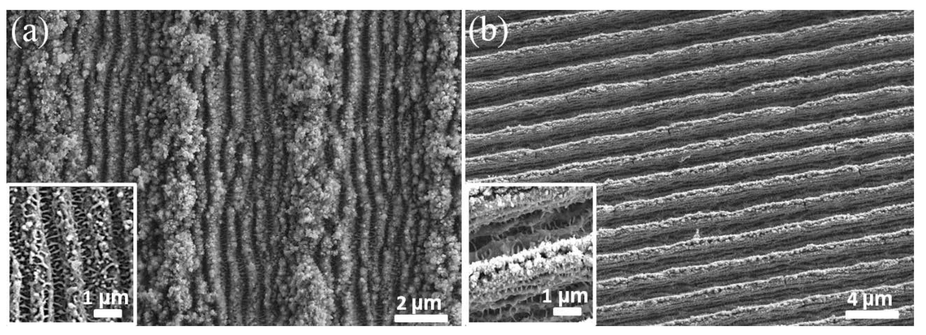
Depending on the parameters used to irradiate the materials, very different surface topologies can be obtained. For instance, the pulse-to-pulse overlap has shown to have significant effect on the height of the produced patterns. This effect is shown exemplary in Figure 5, for the case of line-like periodic arrays produced in ferritic steel and Ti6Al4V using high pulse-to-pulse overlaps in Figure 5a,b, respectively. For the irradiation process, a picosecond pulsed laser system (10 ps) was used and the overlapping angle was varied to obtain 5.2 µm and 2.9 µm periods for Figure 5a,b, respectively. For both materials, a pulse-to-pulse overlap value of 99% was used as well as a laser fluence of 1.42 J/cm². In addition to the very well defined periodic line-like patterns, additional repetitive features can be observed on both materials. The nanostructures mostly visible at the interference maxima positions of the DLIP structures consist of periodical features which can be classified as to different types of laser-induced periodic surface structures (LIPSS) [36]. The features observed parallel to the DLIP structures correspond to low spatial frequency LIPSS (LSFL) with a spatial period of approximately 800 nm, which is similar to the used laser wavelength (1064 nm). In addition, also high spatial frequency LIPSS (HSFL) can be observed (see inset in Figure 5a), but in this case they are perpendicular to the DLIP structures with a spatial period of approximately 200 nm. The same features could be observed in the irradiated Ti6Al4V (see inset in Figure 5b) with similar feature sizes. The orientation of both LSFL and HSFL are related to the direction of the polarization of the laser radiation. While the LSFL are in general oriented perpendicular to the beam polarization, the HSFL are parallel oriented which is in good agreement with the literature [37].
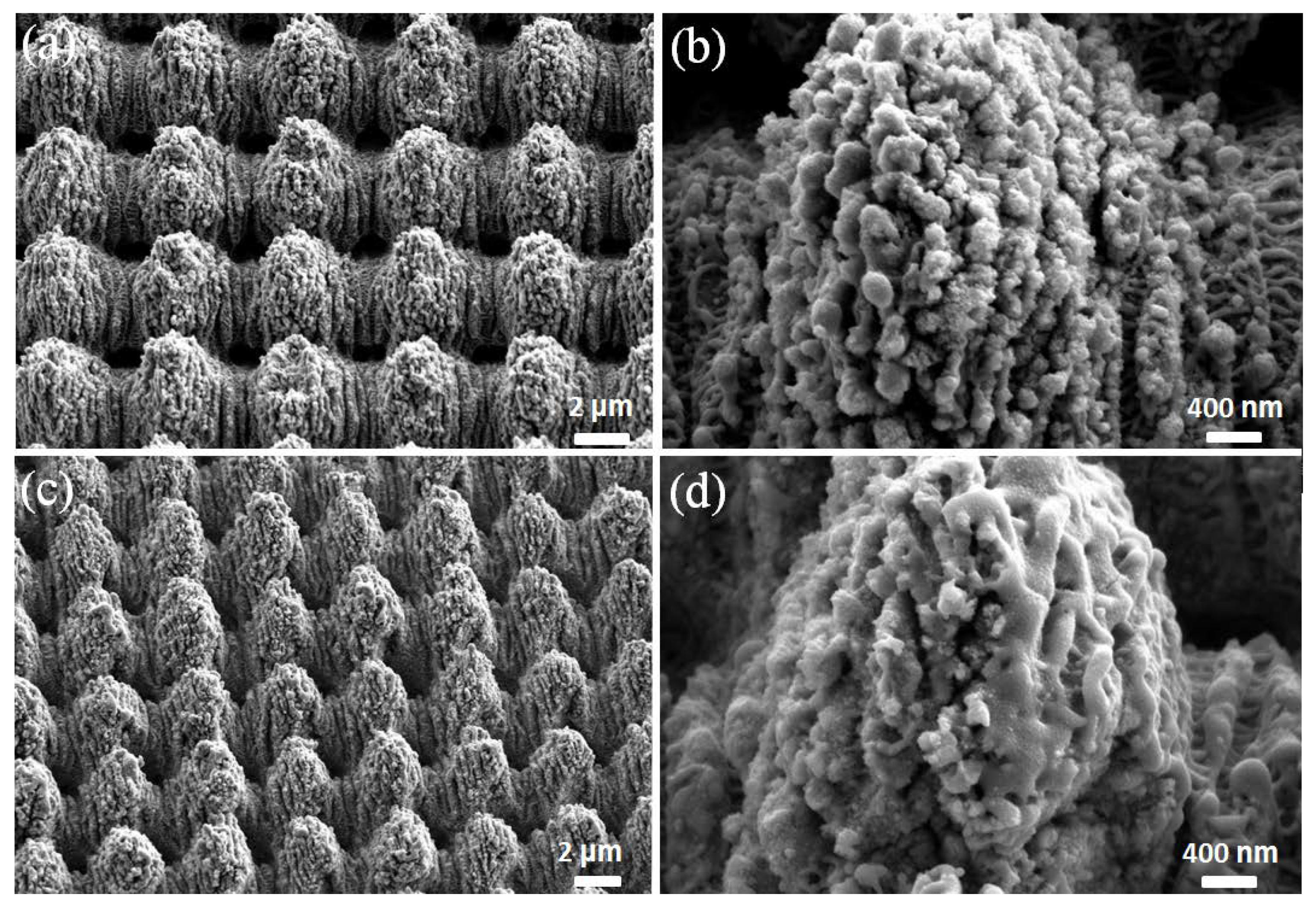
In addition to line-like patterns, using two-beam DLIP, also pillar like patterns can be produced, using the procedure previously described for the polymer materials. Examples of these structures are shown in Figure 6 on ferritic steel and Ti6Al4V, using picosecond (10 ps) IR (1064 nm) radiation. Additional information about the methodology employed can be found in [37]. Also in this case, the pulse-to-pulse overlap was set to 99%. The spatial period for both materials was 5.2 µm and a laser fluence of 1.42 J/cm² was used. The used spatial period is similar to the feature sizes observed in the Colocasia esculenta surface, with super-hydrophobic properties [38]. The DLIP treatment at the mentioned conditions allowed achieving depths of 5.0 ± 0.5 µm and 4.2 ± 0.3 µm on ferritic steel and Ti6AlV4, respectively. Consequently, aspect ratios (ratio between structure depth and spatial period) of 0.96 and 0.80 were achieved, for a total cumulative fluence of 284 J/cm². The last value clearly shows the high amount of energy per unit of area that is required for fabricating high-aspect ratio patterns using ps-laser sources. However, they are comparable with other experiments in the literature for instance involving direct laser writing, where cumulated fluences up to ~400J/cm² have been reported for producing patterns with relative high aspect ratios (~1–2) [15]. Similarly, cone-like or spike-like geometries (corresponding to LIPSS morphologies) with high aspect ratio also required of high cumulated fluence vales (e.g., 300 pulses with ~1 J/cm² = 300 J/cm², for steel) [18]. Like in the line-like patterns, also LSFL and HSFL were observed, but because of their orientation it can be assumed that they were fabricated during the second irradiation step.
Finally, water contact angle (WCA) measurements of the produced pillar-like patterns were performed. In the case of the ferritic steel substrate, a WCA of 5° was measured directly after the laser process denoting a hydrophilic character of the surface. For the Ti6Al4V material, a similar behavior was observed, with a WCA of 30°. However, after 30 days, the WCA significantly increased for both surfaces up to 120° and 76° for the ferritic steel and Ti6Al4V, respectively. This increase has been observed not only for DLIP but also other laser based processing methods and has been explained in relation with an increasing amount of carbon in the processed surface when exposed in normal environment conditions [39]. In other materials such stainless steel, contact angles over 160° could be obtained denoting also the importance of the material and thus the surface chemistry [37].
The relatively long depth of interference field provides the ability to structure not only rough surfaces but also the tilted surface that result in the structure with asymmetrical topography. An example of such structure formed by DLIP on ferritic steel is showed in Figure 7b. The structure was formed by scanning the 2 beam interference spot of 83 µm in diameter across the tilted by 45° surface and keeping the overlap of 97% between the spots. The picosecond laser emitting pulses of 70 ps at 1 kHz repetition rate with the fluence of 0.87 J/cm² was applied in this case.
The topography cross-section of the fabricated structure measured with confocal microscope is plotted in Figure 7a. It can be seen, that the resultant structure contains periodic line-like grooves formed of inclined planes. The plane inclination angle of 7° was measured (note that the scales in Figure 7a are different). As can be seen from the magnified SEM image of the single inclined plane (Figure 7c) the formation of the previously mentioned LIPSS oriented perpendicularly to the direction of the structure is observed on top of those planes. The measured period of these LIPSS was in this case ~886 ± 50 nm, which is close to the used laser wavelength of 1064 nm and therefore corresponds to the low spatial frequency LIPSS (LSFL). The high spatial frequency LIPSS (HSFL) with the period of 180 ± 30 nm was also found in between the grooves of the LSFL (see inset of Figure 7c).
Taking into account all different scale structures formed in this case, the overall morphology of such multiscale-structure can be attributed to the hierarchical structure with asymmetrical topography. The resultant asymmetry of the topography alters the isotropy of the induced functional properties, conferring them directional properties, which, for example, can be used to transport water droplets and soft materials, control liquid spreading, provide directional adhesion and exhibit directional friction [40].
3.4. Industrial System for Direct Laser Interference Patterning
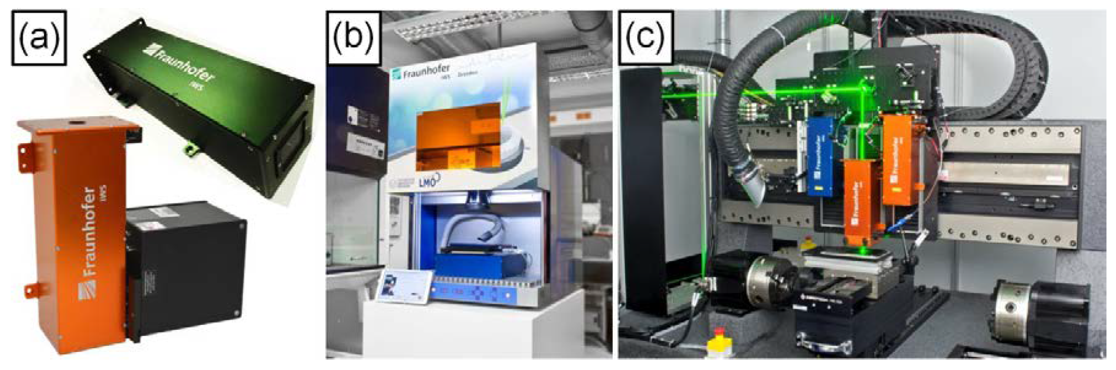
In order to meet particular requirements of industrial environments, different concepts for interference structuring have been developed (see Figure 8a). The high-throughput DLIP module consist on optical system with a cylindrical telescope to expand the laser beam only in one direction, followed by an arrangement for beam splitting and alignment (patented by Fraunhofer IWS, Dresden). Later, a cylindrical lens is used for compressing the laser sub-beams, also only in one direction (details about this optical setup have been published elsewhere [41]). In this way, the module realizes beam shaping to a long drawn line in the focused area, where the interference pattern is obtained. Forming the interfering beams into the shape of long lines has advantages in achieving maximum process speeds. For instance, using a Q-switched slab-type solid-state laser, throughputs up to ~1 m²/min have been already achieved [25]. While conventional laser processing generates only one feature for each single pulse, DLIP allows the simultaneous fabrication of several hundred of features utilizing one single laser pulse. For example, in [25] 682 features were produced per single laser spot. For producing this amount of features using DLW (for example at 300 kHz repetition rate), to achieve feature densities y of ~109 m−2, a maximum processing speed of 0.04 m²/min can be achieved using DLW. These speeds are about 10 to 50 times slower, compared to high-speed DLIP. Clearly, the use of laser systems operating in the MHz range could solve this problem. However, linear speeds over the limits of galvanometer scanners are required (>10 m/s) and simultaneously, the spot diameter over the work piece must be at least 8–10 µm to be comparable with high-speed DLIP. Polygon-scanners are today capable to offer scanning speeds even over 100 m/s. However, their resolution is limited to 24–45 µm (for IR radiation) [42].
Other DLIP optical modules that have been developed enable an individualized control of structure properties (e.g., topographical structure geometry and period). These modules permit an automatized variation of the spatial period and geometry, and thus can be used to fabricate decorative elements.
In recent years, various DLIP systems have been developed. In addition to the DLIP-µFAB system (first prototype developed in 2013), a DLIP galvanometer scanning system was also recently constructed (Figure 8a). In this way, a significant improvement of the process speed due to the low inertia of the galvanometer mirrors compared to translational stages can be obtained. The scanner-based DLIP optical head permits to reach throughputs of several cm² per min (e.g., 12 and 60 cm²/min for 2 and 10 KHz repetition rates). Furthermore, these optical heads have been already integrated into prototype system (DLIP-cube) as shown in Figure 8b. For the case when larger parts must be treated, a special DLIP system (developed at the TU-Dresden, Dresden, Germany) can be also used (Figure 8c). This system permits to treat cylindrical parts up to 600 mm in length and 300 mm in diameter. The system can be equipped with both ns and ps-laser systems and similarly like in the DLIP-μFAB system, different optical heads can be utilized. Further information about the 3D-DLIP system has been published elsewhere [43].
4. Conclusions
In summary, we could demonstrate the advantages of laser interferometric methods for the fabrication-textured surfaces with multiple-scaled features imitating natural examples. Using different processing strategies, periodic patterns with feature sizes in the range of sub-micrometer up to some micrometers have been produced in different materials using ns and ps pulsed laser systems. While irradiating photoresist and polymers (using ns pulsed laser sources) hierarchical structures can be produced using different processing strategies, in the case of metals, laser induced periodic surface structures could also be obtained, which combined with the DLIP structures, permitted to create a three-level hierarchical topography. Finally, different modular solutions for the processing of 2D and 3D parts have been shortly introduced, demonstrating the maturity that this technology has already reached, opening new opportunities for surface functionalization at the industrial scale.
Author Contributions
Conceptualization, A.F.L., B.V. and T.K.; Methodology, F.R., S.A. and A.I.A.-M.; Software, B.V.; Validation, F.R., S.A., A.I.A.-M.; Writing-Original Draft Preparation, S.A., T.K. and A.F.L.; Writing-Review & Editing, A.F.L.; Supervision, A.F.L.
Funding
The work of S.A. and A.I.A.-M. has been supported by the European Union’s Horizon 2020 research and innovation programme under the Marie Skłodowska-Curie grant agreement No. 675063. The work of A.F.L. and F.R. was carried out in the framework of the Reinhart Koselleck project (LA2513_7-1), supported by the German Research Foundation (German: Deutsche Forschungsgemeinschaft DFG).
Acknowledgments
The authors greatly acknowledge the support of Markus Günther their assistance during the SEM investigations.
Conflicts of Interest
The authors declare no conflict of interest. The founding sponsors had no role in the design of the study; in the collection, analyses, or interpretation of data; in the writing of the manuscript, and in the decision to publish the results.
References
- Reznick, D.A.; Bryga, H.; Endler, J.A. Experimentally induced life-history evolution in a natural population. Nature 1990, 346, 357–359. [Google Scholar] [CrossRef]
- Yoseph, B.-C. Biomimetics: Biologically Inspired Technologies; CRC Press: Boca Raton, FL, USA, 2006; Volume 9, ISBN 0849331633. [Google Scholar]
- Hensel, R.; Helbig, R.; Aland, S.; Voigt, A.; Neinhuis, C.; Werner, C. Tunable nano-replication to explore the omniphobic characteristics of springtail skin. NPG Asia Mater. 2013, 5, e37. [Google Scholar] [CrossRef]
- Oeffner, J.; Lauder, G.V. The hydrodynamic function of shark skin and two biomimetic applications. J. Exp. Biol. 2012, 215, 785–795. [Google Scholar] [CrossRef] [PubMed] [Green Version]
- Zhang, D.Y.; Luo, Y.H.; Li, X.; Chen, H.W. Numerical simulation and experimental study of drag-reducing surface of a real shark skin. J. Hydrodyn. 2011, 23, 204–211. [Google Scholar] [CrossRef]
- Jaroniec, C.P.; Kruk, M.; Jaroniec, M.; Sayari, A. Tailoring surface and structural properties of MCM-41 silicas by bonding organosilanes. J. Phys. Chem. B 1998, 102, 5503–5510. [Google Scholar] [CrossRef]
- Yan, Y.Y.; Gao, N.; Barthlott, W. Mimicking natural superhydrophobic surfaces and grasping the wetting process: A review on recent progress in preparing superhydrophobic surfaces. Adv. Colloid Interface Sci. 2011, 169, 80–105. [Google Scholar] [CrossRef] [PubMed]
- Barthlott, W.; Neinhuis, C. Purity of the sacred lotus, or escape from contamination in biological surfaces. Planta 1997, 202, 1–8. [Google Scholar] [CrossRef]
- Barthlott, W.; Mail, M.; Bhushan, B.; Koch, K. Plant surfaces: Structures and functions for biomimetic innovations. Nano-Micro Lett. 2017, 9, 1–40. [Google Scholar] [CrossRef]
- Wagner, T.; Neinhuis, C.; Barthlott, W. Wettability and contaminability of insect wings as a function of their surface sculptures. Acta Zool. 1996, 77, 213–225. [Google Scholar] [CrossRef]
- Helbig, R.; Nickerl, J.; Neinhuis, C.; Werner, C. Smart skin patterns protect springtails. PLoS ONE 2011, 6, e25105. [Google Scholar] [CrossRef] [PubMed]
- Filippov, A.E.; Gorb, S.N. Modelling of the frictional behaviour of the snake skin covered by anisotropic surface nanostructures. Sci. Rep. 2016, 6, 23539. [Google Scholar] [CrossRef] [PubMed] [Green Version]
- Sharp, M.C.; Rosowski, A.P.; French, P.W. Nanosecond laser texturing of aluminium for control of wettability. Proc. SPIE 2015, 9657, 96570J1–96570J7. [Google Scholar] [CrossRef]
- Razi, S.; Madanipour, K.; Mollabashi, M. Laser surface texturing of 316L stainless steel in air and water: A method for increasing hydrophilicity via direct creation of microstructures. Opt. Laser Technol. 2016, 80, 237–246. [Google Scholar] [CrossRef]
- Del Cerro, D.A.; Marín, Á.G.; Römer, G.R.B.E.; Pathiraj, B.; Lohse, D.; Huis in’t Veld, A.J. Leidenfrost point reduction on micropatterned metallic surfaces. Langmuir 2012, 28, 15106–15110. [Google Scholar] [CrossRef] [PubMed]
- Yong, J.; Chen, F.; Yang, Q.; Hou, X. Femtosecond laser controlled wettability of solid surfaces. Soft Matter 2015, 11, 8897–8906. [Google Scholar] [CrossRef] [PubMed] [Green Version]
- Zorba, V.; Persano, L.; Pisignano, D.; Athanassiou, A.; Stratakis, E.; Cingolani, R.; Tzanetakis, P.; Fotakis, C. Making silicon hydrophobic: Wettability control by two-length scale simultaneous patterning with femtosecond laser irradiation. Nanotechnology 2006, 17, 3234–3238. [Google Scholar] [CrossRef]
- Kam, D.H.; Bhattacharya, S.; Mazumder, J. Control of the wetting properties of an AISI 316L stainless steel surface by femtosecond laser-induced surface modification. J. Micromech. Microeng. 2012, 22, 105019. [Google Scholar] [CrossRef]
- Vorobyev, A.Y.; Guo, C. Direct femtosecond laser surface nano/microstructuring and its applications. Laser Photonics Rev. 2013, 7, 385–407. [Google Scholar] [CrossRef]
- Zwahr, C.; Voisiat, B.; Welle, A.; Günther, D. One-step fabrication of pillar and crater-like structures on titanium using direct laser interference patterning. Adv. Eng. Mater. 2018, 20, 1800160. [Google Scholar] [CrossRef]
- Siebold, M.; Loeser, M.; Röser, F.; Albach, D.; Bussmann, M.; Eckhardt, S.; Lasagni, A.F.; Sauerbrey, R.; Schramm, U. High energy Yb:YAG active mirror laser system for transform limited pulses bridging the picosecond gap. Laser Photonics Rev. 2016, 10, 673–680. [Google Scholar] [CrossRef]
- Aguilar-Morales, A.I.; Alamri, S.; Kunze, T.; Lasagni, A.F. Influence of processing parameters on surface texture homogeneity using direct laser interference patterning. Opt. Laser Technol. 2018, 107, 216–227. [Google Scholar] [CrossRef]
- Kondo, T.; Matsuo, S.; Juodkazis, S.; Misawa, H. Femtosecond laser interference technique with diffractive beam splitter for fabrication of three-dimensional photonic crystals. Appl. Phys. Lett. 2001, 79, 725–727. [Google Scholar] [CrossRef]
- Nakata, Y.; Miyanaga, N.; Okada, T. Effect of pulse width and fluence of femtosecond laser in the size of nanobump array. Appl. Surf. Sci. 2007, 253, 6555–6557. [Google Scholar] [CrossRef]
- Lang, V.; Roch, T.; Lasagni, A.F. High-speed surface structuring of polycarbonate using direct laser interference patterning: Toward 1 m²·min−1 fabrication speed barrier. Adv. Eng. Mater. 2016, 18, 1342–1348. [Google Scholar] [CrossRef]
- Rodriguez, A.; Echeverría, M.; Ellman, M.; Perez, N.; Verevkin, Y.K.; Peng, C.S.; Berthou, T.; Wang, Z.; Ayerdi, I.; Savall, J.; et al. Laser interference lithography for nanoscale structuring of materials: From laboratory to industry. Microelectron. Eng. 2009, 86, 937–940. [Google Scholar] [CrossRef]
- Lasagni, A.F.; Menéndez-Ormaza, B.S. Two- and three-dimensional micro- and sub-micrometer periodic structures using two-beam laser interference lithography. Adv. Eng. Mater. 2010, 12, 54–60. [Google Scholar] [CrossRef]
- Alamri, S.; Lasagni, A.F. Development of a general model for direct laser interference patterning of polymers. Opt. Express 2017, 25, 9603–9616. [Google Scholar] [CrossRef] [PubMed]
- Kunze, T.; Zwahr, C.; Krupop, B.; Alamri, S.; Rößler, F.; Lasagni, A.F. Development of a scanner-based direct laser interference patterning optical head: New surface structuring opportunities. Proc. SPIE 2017, 10092, 1009214. [Google Scholar] [CrossRef]
- Alamri, S.; Aguilar-Morales, A.I.; Lasagni, A.F. Controlling the wettability of polycarbonate substrates by producing hierarchical structures using direct laser interference patterning. Eur. Polym. J. 2018, 99, 27–37. [Google Scholar] [CrossRef]
- Raillard, B.; Rémond, J.; Ramos-Moore, E.; Souza, N.; Gachot, C.; Mücklich, F. Wetting properties of steel surfaces modified by laser interference metallurgy. Adv. Eng. Mater. 2013, 15, 341–346. [Google Scholar] [CrossRef]
- Rosenkranz, A.; Hans, M.; Gachot, C.; Thome, A.; Bonk, S.; Mücklich, F. Direct laser interference patterning: tailoring of contact area for frictional and antibacterial properties. Lubricants 2016, 4, 2. [Google Scholar] [CrossRef]
- Bieda, M.; Siebold, M.; Lasagni, A.F. Fabrication of sub-micron surface structures on copper, stainless steel and titanium using picosecond laser interference patterning. Appl. Surf. Sci. 2016, 387, 175–182. [Google Scholar] [CrossRef]
- Lasagni, A.; D’Alessandria, M.; Giovanelli, R.; Mücklich, F. Advanced design of periodical architectures in bulk metals by means of laser interference metallurgy. Appl. Surf. Sci. 2007, 254, 930–936. [Google Scholar] [CrossRef]
- Indrišiūnas, S.; Voisiat, B.; Gedvilas, M.; Račiukaitis, G. Two complementary ways of thin-metal-film patterning using laser beam interference and direct ablation. J. Micromech. Microeng. 2013, 23, 095034. [Google Scholar] [CrossRef]
- Skolski, J.Z.P.; Römer, G.R.B.E.; Vincenc Obona, J.; Huis In ’T Veld, A.J. Modeling laser-induced periodic surface structures: Finite-difference time-domain feedback simulations. J. Appl. Phys. 2014, 115, 103102. [Google Scholar] [CrossRef]
- Aguilar-Morales, A.I.; Alamri, S.; Lasagni, A.F. Micro-fabrication of high aspect ratio periodic structures on stainless steel by picosecond direct laser interference patterning. J. Mater. Process. Technol. 2018, 252, 313–321. [Google Scholar] [CrossRef]
- Ensikat, H.J.; Ditsche-Kuru, P.; Neinhuis, C.; Barthlott, W. Superhydrophobicity in perfection: The outstanding properties of the lotus leaf. Beilstein J. Nanotechnol. 2011, 2, 152–161. [Google Scholar] [CrossRef] [PubMed]
- Kietzig, A.M.; Hatzikiriakos, S.G.; Englezos, P. Patterned superhydrophobic metallic surfaces. Langmuir 2009, 25, 4821–4827. [Google Scholar] [CrossRef] [PubMed]
- Hancock, M.J.; Sekeroglu, K.; Demirel, M.C. Bioinspired directional surfaces for adhesion, wetting, and transport. Adv. Funct. Mater. 2012, 22, 2223–2234. [Google Scholar] [CrossRef] [PubMed]
- Lang, V.; Hoffmann, T.; Lasagni, A.F. Optimization for high speed surface processing of metallic surfaces utilizing direct laser interference patterning. In Proceedings of the SPIE Laser-Based Micro- and Nanoprocessing XII, San Francisco, CA, USA, 19 February 2018; Volume 10520, p. 105200K-1. [Google Scholar] [CrossRef]
- Loeschner, U.; Schille, J.; Streek, A.; Knebel, T.; Hartwig, L.; Hillmann, R.; Endisch, C. High-rate laser microprocessing using a polygon scanner system. J. Laser Appl. 2015, 27, S29303. [Google Scholar] [CrossRef]
- Lang, V.; Rank, A.; Lasagni, A.F. Large area one-step fabrication of three-level multiple-scaled micro and nanostructured nickel sleeves for roll-to-roll hot embossing. Adv. Eng. Mater. 2017, 19, 1700126. [Google Scholar] [CrossRef]
Figure 1.
SEM images of (a) 5 µm hexagonal hole-like structure on top of a 0.5 µm hole-like structure, (b) the same with a larger magnification. (c) 5 µm hole-like structure covered with 0.5 µm of spatial period pattern and (d) 5 µm and 0.5 µm exposure consecutively in the same layer. In all cases, 7.5 mJ/cm² and 4 mJ/cm² were used for the 5 and 0.5 µm pattern, respectively.
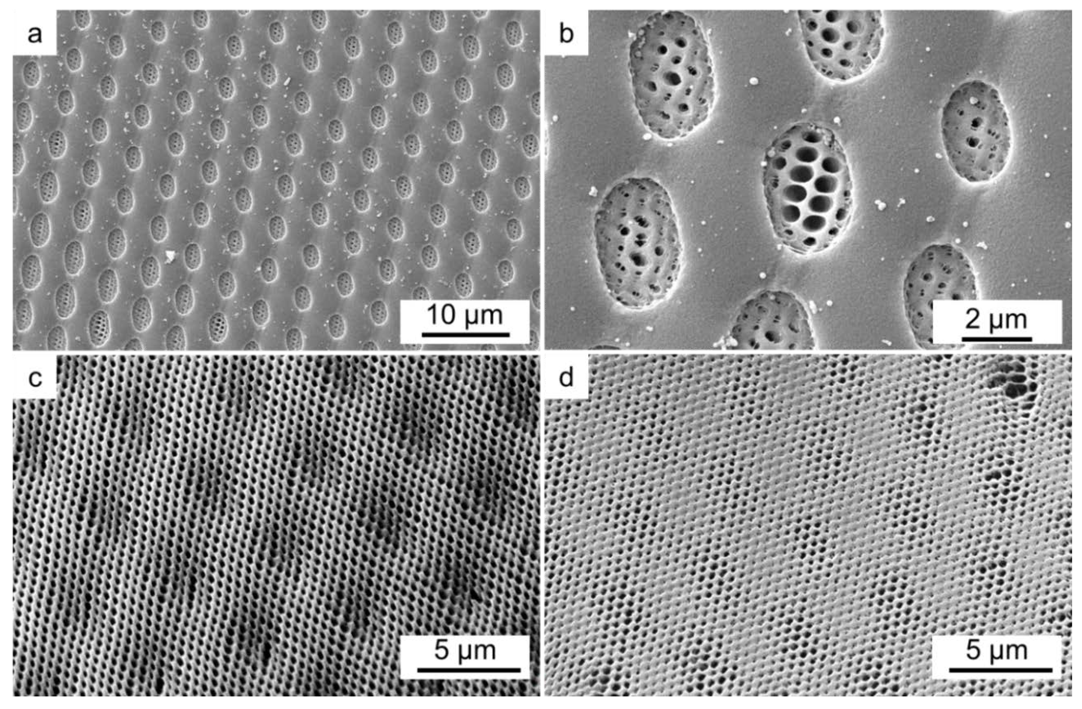
Figure 2.
AFM pseudo-color images of (a,b) 5 µm on 0.5 µm hierarchical patterns (using two layers of resist), (c,d) 0.5 µm pattern on top of 5 µm pattern (also using two layers of resist) and (e,f) 5 µm and 0.5 µm hole-like patterns exposed in a single layer of SU-8 resist.
Figure 2.
AFM pseudo-color images of (a,b) 5 µm on 0.5 µm hierarchical patterns (using two layers of resist), (c,d) 0.5 µm pattern on top of 5 µm pattern (also using two layers of resist) and (e,f) 5 µm and 0.5 µm hole-like patterns exposed in a single layer of SU-8 resist.
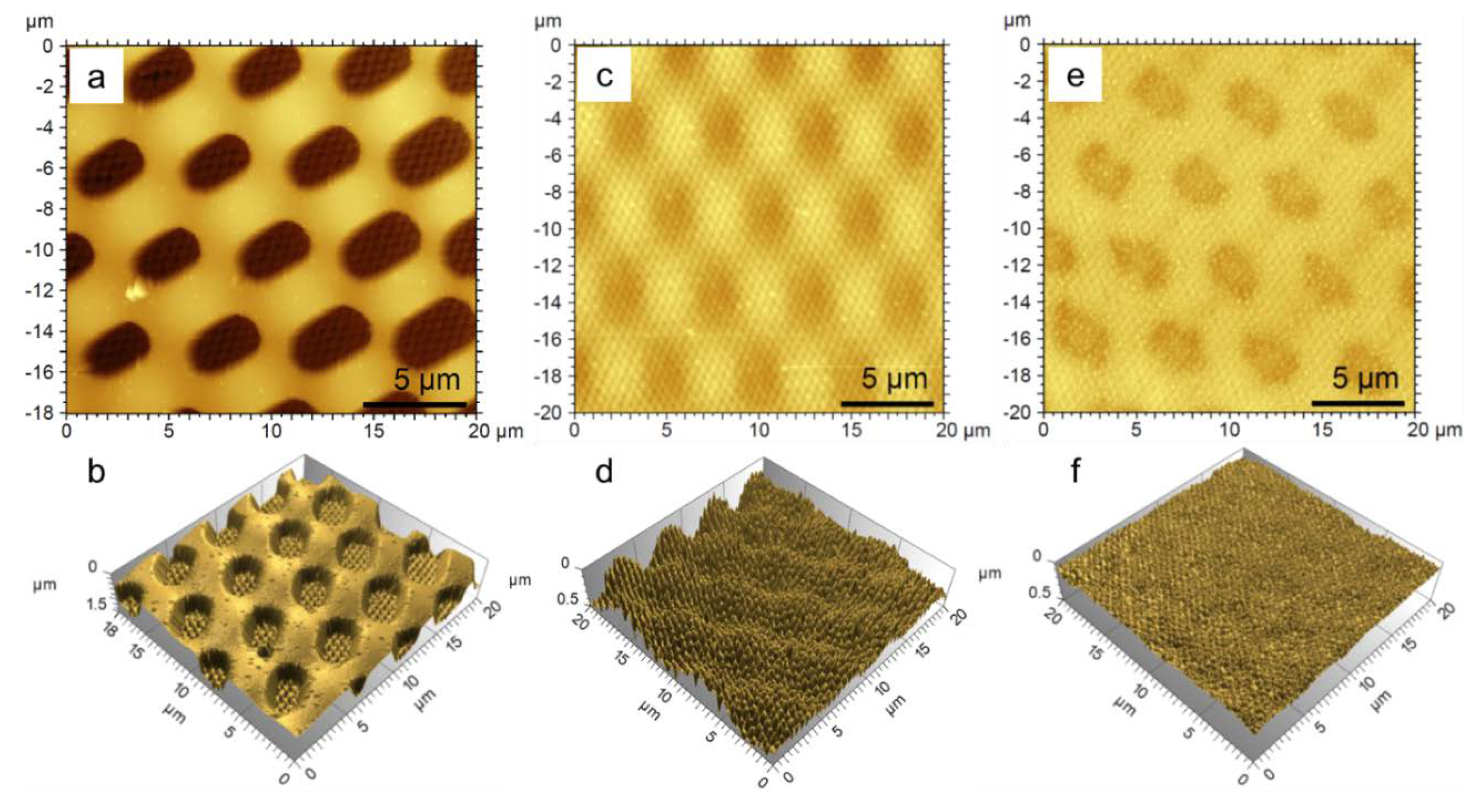
Figure 3.
(a) Top-view SEM image of the hierarchical line-like on line-like structures parallel oriented, (b) line-like on line-like structures perpendicularly oriented, (c) line-like structures on pillars before cleaning, (d) line-like structures on pillars after cleaning, (e) pillar-like on pillar-like structures and (f) details of the hierarchy of pillar-like on pillar-like structures [30].

Figure 4.
Water contact angle response measured in orthogonal directions for the different pulse-overlap conditions, for anisotropic line-like on pillars structures (a) and isotropic pillars on pillars structures (b) [30].
Figure 4.
Water contact angle response measured in orthogonal directions for the different pulse-overlap conditions, for anisotropic line-like on pillars structures (a) and isotropic pillars on pillars structures (b) [30].
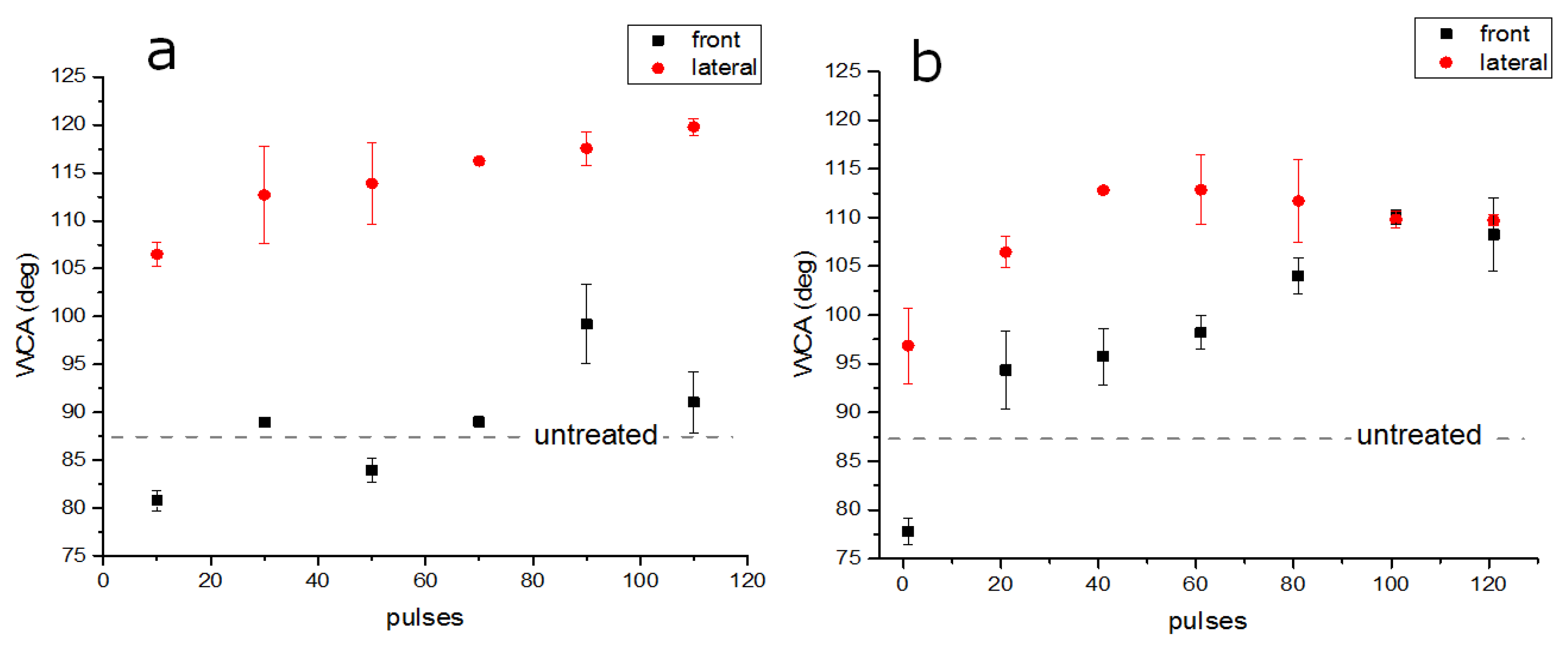
Figure 5.
Line-like periodic structures fabricated by Direct Laser Interference Patterning using a laser fluence of 1.42 J/cm² and 99% of pulse-to-pulse overlap on (a) ferritic steel (with an spatial period of 5.2 µm) and (b) on Ti6Al4V (with and spatial period of Λ = 2.9 µm). The insets show the appearance of HSFL. LSFL can be also observed, mainly at the positions corresponding to the interference maxima.

Figure 6.
Pillar-like structures fabricated by Direct Laser Interference Patterning on (a,b) ferritic steel and (c,d) Ti6Al4V substrates. The selected spatial period was 5.2 µm. For the process, the laser fluence was fixed to 1.42 J/cm2 and a pulse-to-pulse overlap of 99% was used.
Figure 6.
Pillar-like structures fabricated by Direct Laser Interference Patterning on (a,b) ferritic steel and (c,d) Ti6Al4V substrates. The selected spatial period was 5.2 µm. For the process, the laser fluence was fixed to 1.42 J/cm2 and a pulse-to-pulse overlap of 99% was used.

Figure 7.
Profile of the structure formed by 2 beam DLIPs of substrate tilted by 45° and corresponding SEM images of the same area.
Figure 7.
Profile of the structure formed by 2 beam DLIPs of substrate tilted by 45° and corresponding SEM images of the same area.
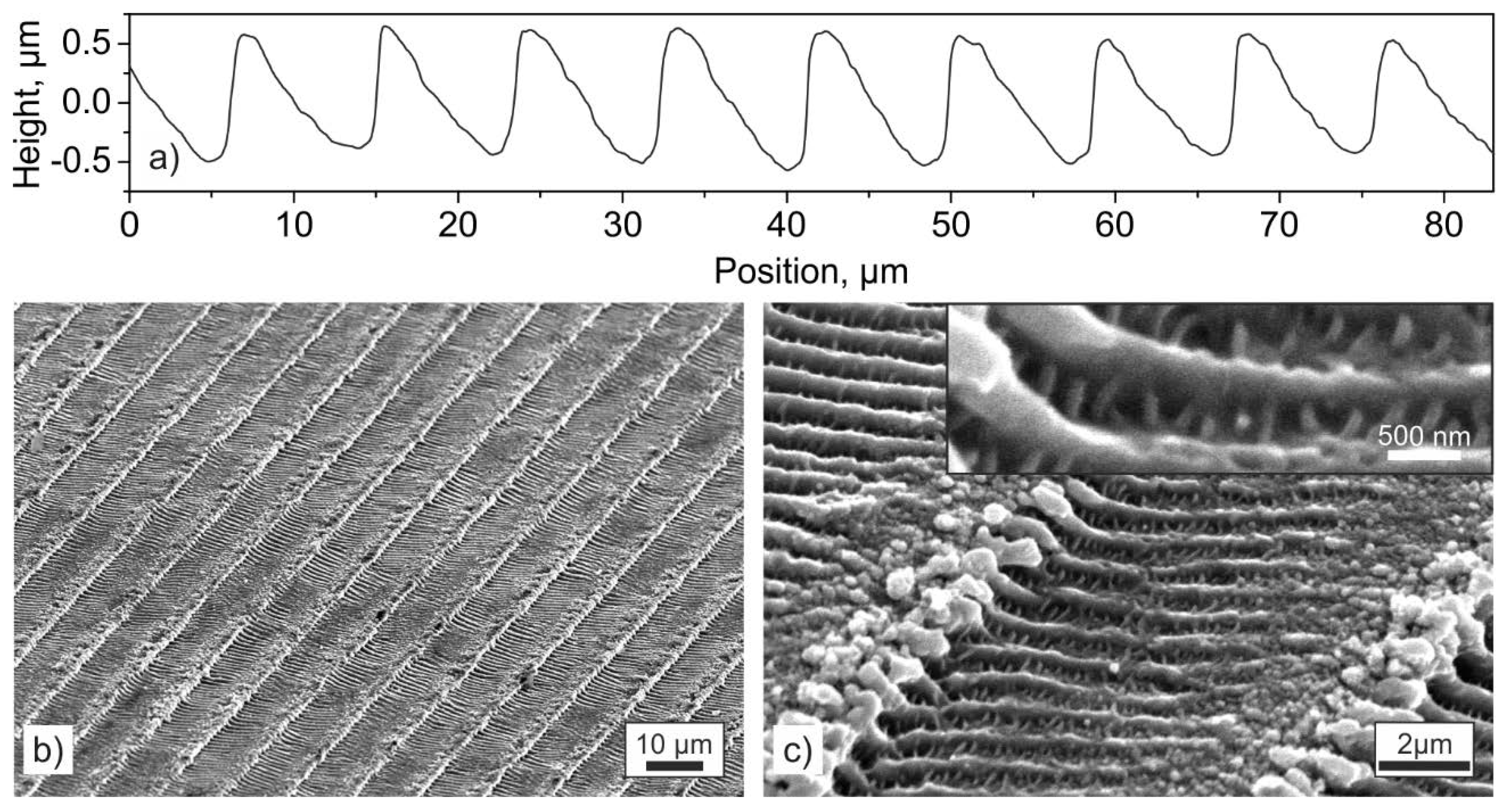
Figure 8.
(a) High-throughput (green) and scanner-based (orange) DLIP optical heads; (b) DLIP-cube system with integrated scanner DLIP optics; (c) large area DLIP system for 2D and 3D parts (TU-Dresden, Fraunhofer IWS). The system consists of three different DLIP optics and utilizes a solid-state ps-laser.

© 2018 by the authors. Licensee MDPI, Basel, Switzerland. This article is an open access article distributed under the terms and conditions of the Creative Commons Attribution (CC BY) license (http://creativecommons.org/licenses/by/4.0/).
Share and Cite
MDPI and ACS Style
Lasagni, A.F.; Alamri, S.; Aguilar-Morales, A.I.; Rößler, F.; Voisiat, B.; Kunze, T. Biomimetic Surface Structuring Using Laser Based Interferometric Methods. Appl. Sci. 2018, 8, 1260. https://doi.org/10.3390/app8081260
AMA Style
Lasagni AF, Alamri S, Aguilar-Morales AI, Rößler F, Voisiat B, Kunze T. Biomimetic Surface Structuring Using Laser Based Interferometric Methods. Applied Sciences. 2018; 8(8):1260. https://doi.org/10.3390/app8081260
Chicago/Turabian StyleLasagni, Andrés Fabián, Sabri Alamri, Alfredo Ismael Aguilar-Morales, Florian Rößler, Bogdan Voisiat, and Tim Kunze. 2018. "Biomimetic Surface Structuring Using Laser Based Interferometric Methods" Applied Sciences 8, no. 8: 1260. https://doi.org/10.3390/app8081260
Note that from the first issue of 2016, this journal uses article numbers instead of page numbers. See further details here.