Abstract
Monolayer (1L) transition-metal dichalcogenides (TMDCs) are attractive materials for several optoelectronic applications because of their strong excitonic resonances and valley-selective response. Valley excitons in 1L-TMDCs are formed at opposite points of the Brillouin zone boundary, giving rise to a valley degree of freedom that can be treated as a pseudospin, and may be used as a platform for information transport and processing. However, short valley depolarization times and relatively short exciton lifetimes at room temperature prevent using valley pseudospins in on-chip integrated valley devices. Recently, it was demonstrated how coupling these materials to optical nanoantennas and metasurfaces can overcome this obstacle. Here, we review the state-of-the-art advances in valley-selective directional emission and exciton sorting in 1L-TMDC mediated by nanostructures and nanoantennas. We briefly discuss the optical properties of 1L-TMDCs paying special attention to their photoluminescence/absorption spectra, dynamics of valley depolarization, and the valley Hall effect. Then, we review recent works on nanostructures for valley-selective directional emission from 1L-TMDCs.
1. Introduction
As the growth of electronics and computing infrastructure nears the limits of the so-called Moore’s law [1], new directions in information processing and harvesting become of crucial importance in today’s technology. This issue inspired new fields of research, such as spintronics and valleytronics, in which spin or pseudospin is used as an alternative information carrier. Currently, valleytronics is of great interest due to the discovery of atomically thin single-layered (1L) transition-metal dichalcogenides (TMDCs) [2,3,4,5,6,7,8,9,10,11,12,13,14]. Monolayer TMDCs are formed (Figure 1a) by a hexagonal network of transition metal atoms (M: Mo, W) hosted between two hexagonal lattices of chalcogenide atoms (X: S, Se). Electronically, 1L-TMDCs behave as two-dimensional semiconductors, with bandgaps lying in the visible and near-infrared (IR) range. In the monolayer limit, the bandgaps of these materials are direct, enabling enhanced interactions of dipole transitions with light. An essential property of 1L-TMDCs is the broken inversion symmetry of their hexagonal 2D crystals, which, in combination with time-reversal symmetry, leads to opposite spins at the +K and −K valleys, effectively locking the spin and valley degrees of freedom (pseudospin or Berry curvature) [15,16,17]. Optical manipulation of the valley degree of freedom can be realized via exciton resonances based on the valley contrasting optical selection rules (for instance with and light excitation). The unique opportunity of addressing the valley index makes it possible to explore this binary quantum degree of freedom as an alternative information carrier [12,18,19,20], which may complement both classical and quantum computing schemes based on charge and spin. This possibility of using the valley degree of freedom for information processing and storage (similar to spin in spintronics) leads to conceptually new applications for valleytronics [12].
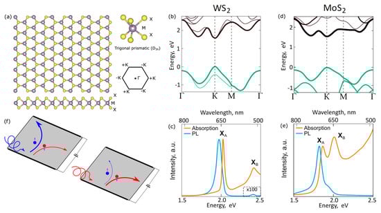
Figure 1.
(a) Monolayer (1L) transition-metal dichalcogenide crystal (TMDC) structure. Transition-metal atoms (M) appear in purple, and chalcogen atoms (X) are in yellow. The structure resembles that of graphene, but with broken inversion symmetry. A side view shows the three-dimensional (3D) structure. The hexagonal Brillouin zone is shown with the Γ point and the two inequivalent +K and −K points. (b) Energy structure of 1L-WS2; blue and black curves demonstrate the valence and conduction bands. (c) Absorption spectrum (orange curve) and photoluminescence (blue curve) of 1L-WS2 at room temperature. (d,e) The same for MoS2. (f) Valley Hall effect. Blue (red) denotes the electron in valley +K (−K). The purple arrows indicate the pseudo-vector quantities (Berry curvature or orbital magnetic moment) of the electron (hole); blue and red spirals indicate and light excitation.
However, short valley depolarization times and relatively short exciton lifetimes at room temperature prevent using valley pseudospin in on-chip integrated valley devices. Recently, it was demonstrated how coupling these materials to optical nanoantennas and metasurfaces can overcome this obstacle. It was demonstrated that resonant optical nanostructures and nanoantennas can effectively enhance and direct the emission from opposite valleys in 1L-TMDCs into different directions [21,22,23,24]. The proposed nanostructures for valley-selective directional emission can be divided into two groups: nanostructures for spatial separation of valley degrees of freedom using surface waves, and for separation in momentum-space, based on which photons with opposite helicity are emitted in different directions. Spatial separation of valley degrees of freedom may be accompanied by division of valley excitons in space [24], or transformation of valley exciton pseudospin to photonic degrees of freedom (e.g., transverse optical spin angular momentum) via optical spin–orbit coupling [23] (or both these processes).
This paper is devoted to reviewing state-of-the-art advances in 1L-TMDC valley degree-of-freedom separation (valley-selective directional emission and exciton sorting) mediated by nanostructures and nanoantennas. The paper is organized as follows: in Section 2, we briefly discuss the optical properties of two-dimensional (2D) TMDC materials, paying special attention to their photoluminescence/absorption spectra, dynamics of valley depolarization, and the valley Hall effect; in Section 3, we summarize recent published work devoted to nanostructures for 1L-TMDC valley separation. Special attention is devoted to our and our collaborators’ recent results in this area.
2. Optical Properties of 1L-TMDCs
In this section, we briefly discuss the optical properties of 2D-TMDCs, addressing the interested reader to more detailed review papers on the topic [4,7,9,25,26,27]. Single-layered TMDCs (like MoS2, MoSe2, WS2, and WSe2) behave as two-dimensional semiconductors, with their bandgaps lying in the visible and near-infrared (IR) ranges [7]. In the monolayer limit, TMDCs are particularly interesting because their bandgaps become direct, thus enabling enhanced interactions of dipole transitions with light [28]. The evolution of the band structure of 2D-TMDCs was calculated from first principles (density functional theory) in Reference [13]. The transition to a direct bandgap semiconductor makes it easier for photons with an energy equal to the bandgap to be absorbed or emitted, without requiring additional phonons to be absorbed. As a result, the resonant excitonic absorption of a single TMDC monolayer can be as large as 5–20%, which is one order of magnitude larger than, for instance, that of quantum well systems [29]. Experimentally, researchers verified the monolayer nature of chemical vapor deposition (CVD)-grown or exfoliated TMDCs using atomic force microscopy and photoluminescence (PL) spectroscopy [30]. For example, Figure 1b–e demonstrate the band structures of 1L-WS2 (b) and 1L-MoS2 (d), as well as their absorption spectra and photoluminescence (Figure 1c,e) at room temperature. The PL spectrum consists of two resonances corresponding to XA and XB excitons, but the PL emission from the XB exciton is very weak. We note that the optical properties of 1L-TMDCs (PL spectra, Raman spectra, and transmission/absorption spectra) may slightly depend on several factors, including fabrication techniques (mechanical exfoliation or chemical vapor deposition), type of substrate, defects, and others.
Reduced dielectric screening and strong Coulomb interactions between charged particles (electrons and holes) result in strong excitonic resonances in the visible and near-IR range with large binding energies. Strong Coulomb interactions in these materials lead to the formation of strongly bound excitons (binding energies of 0.2 to 0.8 eV) [31,32,33], charged excitons (trions) [34,35], and excitonic molecules (biexcitons) [36,37,38,39,40]. Localized and dark excitonic states in 1L-TMDCs were also demonstrated [36,41,42]. Due to the monolayer nature of 1L-TMDCs, their high oscillator strength, and their potential for tuning, these materials become a unique class of 2D materials for optoelectronic applications, such as photodetection and light harvesting [43,44,45,46], phototransistors and modulation [47,48], and light-emitting diodes [49,50,51]. Operation of 1L-TMDCs in a single-photon emission regime was also reported [52,53]. The enhancement of the exciton transition dipole in 1L-TMDCs can be understood assuming that it is proportional to the electron–hole overlap in real space. Recently, it was demonstrated that the bright-exciton dipole moment can be further enhanced via the dielectric screening effect in high-dielectric-constant solvents (like ethanol and water), which gives rise to asymmetric Fano resonance and strong coupling effects [30]. The quantum yield of emission of these materials depends on many factors, including fabrication techniques (mechanical exfoliation or chemical vapor deposition), type of substrate, defects, and so on. Typically, as-prepared 1L-TMDCs have a relatively low quantum yield of ~0.1–10% [25]. These low values can be significantly improved (up to ~95%) via chemical treatment with organic superacids [54,55], or via their coupling to specifically tailored resonant optical nanocavities and metasurfaces [42,56,57,58,59,60,61,62,63,64,65,66,67,68,69,70].
A variety of new optical effects stemming from the interaction of 1L-TMDCs with plasmonic (i.e., made of noble metals) and high-index dielectric (Si, Ge, GaP) nanocavities was demonstrated. Examples include the observation of strong plasmon–exciton coupling [63,70,71,72], pronounced Fano resonances [58], and plasmon-induced resonance energy transfer [73], which are very attractive for various quantum optics and nanophotonic applications. These effects benefit from the localization of light within plasmonic and dielectric resonators, enabled by their small mode volumes and the strong dipole moment of excitons in 1L-TMDCs.
Direct bandgap transitions in 1L-TMDCs occur at the energy-degenerate K (K’) points at the edges of the 2D hexagonal Brillouin zone (schematically shown in Figure 1a). Due to inversion symmetry breaking and strong spin–orbital coupling in 1L-TMDCs, the electronic states of the two valleys have different chirality, which leads to valley-selective circular dichroism [15,17,74,75,76,77]. This effect is key for valleytronics applications, which focus on the manipulation of valley pseudo-spins to encode signals and information [12,23,77,78]. The operation principles of valleytronics are mainly based on the valley Hall effect [75], which refers to the opposite Hall currents for carriers located in opposite valleys (Figure 1f). Excitation of 1L-TMDCs by and light causes a nonequilibrium population of the +K or −K valley. These carriers have opposite Berry curvature, which acts like an effective magnetic field in the momentum space. As a result, these two sorts of valley particles (+K or −K) propagate in different directions. If the particles are electrically charged (electrons, holes, or trions), this effect gives rise to the Hall voltage. If the particles are neutral, the Hall effect can be detected by measuring the circularly polarized components of the emitted photoluminescence (PL) intensity. In this case, the effect can be characterized by the degree of valley polarization:
where and refer to the PL intensity with and polarization, respectively. The Hall effect can also be detected in reflectance experiments via so-called Kerr rotation spectroscopy, when a system illuminated by linearly polarized light causes a rotation of polarization in a scattered signal [79,80,81]. By spatially resolving the Kerr signal, the valley polarization can be mapped out in a sample, and accumulation of the +K and −K valley polarizations can be observed.
A general scheme for generating and detecting valley polarization was first proposed and realized in another 2D material—graphene—with broken inversion symmetry [82,83]. Then, a free-carrier valley Hall effect in monolayer MoS2 was demonstrated using electric readout methods [75] in the form of transverse motions of valley-polarized carriers in the presence of an in-plane electric field. More recently, an exciton valley Hall effect was reported for a monolayer MoS2 where the exciton motion was driven by a temperature gradient [77]. Moreover, other factors such as uncontrolled strain can also lead to the separation of valley-polarized excitons [12]. More recently, the valley-polarized exciton dynamics in a 2D semiconductor van-der-Waals heterostructure was also studied and was proven to be a versatile platform for valleytronics [84].
For a full description and understanding of 1L-TMDC behavior, it is important to know the exciton and coherence lifetimes. The exciton lifetime describes the average time for which an exciton exists, and it usually defines the excitonic spectral linewidth. This time also limits the propagation distance of excitons. The coherence time defines the time during which an exciton remembers the state of the excitation field (for example, polarization) [85]. If the system is excited by or light, the coherence lifetime says how long the +K or −K valley is inequivalently polarized (nonzero valley polarization). In 1L-TMDCs, the coherence time is usually less than the exciton lifetime (at room temperature), and it is key for valleytronics and quantum-optics applications [86]. The dynamics of photoexcited electron−hole pairs in 1L-WSe2 at room temperature and ambient conditions was directly traced in Reference [87]. It was shown that, after highly nonresonant interband excitation by a femtosecond laser pulse, the concentration of free carriers increased, reaching its maximum after 0.5 fs. This excitation was followed by a rapid carrier relaxation toward the respective band minima. More than half of the carriers are already bound into excitons 0.4 ps after the excitation. The ratio between excitons and unbound electron–hole pairs increases up to 0.5 ps. Interestingly, the exciton concentration grows even after 0.5–0.6 ps, when the free-carrier concentration starts decaying, and it continues up to 1 ps. Then, both concentrations decay on a time scale of a few picoseconds, while a significant fraction of free carriers is still observed after 5 ps. We note that the results for cryogenic temperatures are similar because of strong binding energies (~0.5 eV) of excitons, which are well above the thermal energy (~50 meV).
The valley-polarization degree dynamics of 1L-WSe2 was experimentally studied in Reference [79] using the pump–probe Kerr rotation technique. It was demonstrated that the exciton valley depolarization time decreased significantly from ~6 ps to ~1.5 ps when the lattice temperature increased from 4 K to 125 K, which is in good agreement with theoretical estimations [88]. In Reference [81], these results were obtained from ab initio calculations, which took into account all possible mechanisms of valley depolarization. Similar results were demonstrated in Reference [41]. At room temperature, the valley depolarization times are considerably shorter than 1 ps, which is much shorter than the exciton lifetime. Thus, all previously reported carrier and exciton valley Hall effects relying on nonzero valley polarization were observed at low temperatures. At room temperature, the valley-polarization lifetime is too short to be utilized in real applications. However, since the binding energy of excitons is very large in 1L-TMDCs, it is, therefore, both feasible and highly desirable to design a photonic device to manipulate valley excitons at room temperature, even without valley polarization. These structures are reviewed in the next section.
3. Nanostructures for Valley-Selective Directional Emission
3.1. Single Nanoantennas
As mentioned in the introduction, the proposed nanostructures for valley-selective response can perform spatial separation of the valley degree of freedom with surface waves or separation in K-space when photons with opposite helicity are emitted in different directions. Moreover, spatial separation of the valley degree of freedom may be accompanied by real dividing of valley excitons [24] or the transformation of valley exciton pseudospin to photonic degrees of freedom via optical spin–orbit coupling [21,23,89,90,91,92] (or both these processes). Below, we describe all these possibilities with various examples from the recent literature.
Photons as information carriers are more robust and controllable than excitons, especially at room temperature. Thus, nanostructures supporting the coupling of valley pseudospin to photonic degrees of freedom (e.g., transverse optical spin angular momentum, t-OSAM) are desirable for on-chip integrated valley devices. The optical spin–orbit coupling effect provides a robust one-to-one transformation of the valley degree of freedom into t-OSAM because of spin-momentum locking. One realization of this idea was implemented in Reference [23] (Figure 2a).
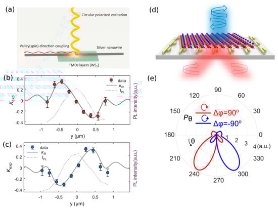
Figure 2.
(a) Conceptual illustration of the directional emission of valley-polarized exciton in WS2. The valley pseudospin and photon path are coupled by the means of spin–orbit coupling of light [23]. (b,c) Measured directional coupling efficiency, , of the guided emission as a function of the position of the excitation 594-nm laser in the transverse direction (y) with (b) left- and (c) right-handed circular polarization. Gray lines represent fitting results obtained using the calculated directional coupling efficiency. Purple dotted lines correspond to the total photoluminescence (PL) intensity measured from the ends of the nanowire as a function of the excitation position. (d) Array of double-bar plasmonic antennas for valley-selective directional emission from a 1L-TMDC. (e) Polar plots of the radiated power in the far field; denotes right and left circularly polarized excitons [22].
The structure consists of a single silver nanowire placed on top of a TMD flake (WS2), consisting of five layers, which is an indirect semiconductor, but still preserves valley-polarization properties [93]. The silver nanowire supports guided modes possessing t-OSAM in the out-plane direction. Spin-momentum locking of these plasmonic modes allows the transformation of valley polarization into directional emission: the system, excited by circularly polarized light in the center of the nanowire, launches plasmonic modes carrying t-OSAM in the left or right direction as a function of their valley polarization. Note that, because of the structure symmetry, this operation can be achieved under asymmetric-laser-spot excitation in the transverse direction (y). This effect can be described by the coupling efficiency, , where and are the light intensities directed to the left and right side, respectively. Thus, when this value is zero, the structure shows the same coupling on both sides. The measurement results of the coupling efficiency for 594-nm and light excitation as a function of the laser-spot coordinate in the transverse direction are shown in Figure 2b,c. The purple dotted lines show the total PL intensity measured from the ends of the nanowire as a function of the excitation position.
Plasmonic (Au) nanoantennas for valley-dependent far-field emission (separation in K-space) when photons with opposite helicity are emitted in different directions were theoretically proposed in Reference [22] (Figure 2d). The antenna consists of two closely arranged plasmonic bars different in their lengths. The short bar possesses electric-dipole resonance, while the longer one has quadrupole resonance at the same operation wavelength. The entire nanoantenna being excited by a circularly polarized dipole (modeled as two orthogonal short dipoles with a relative phase of ) emits in different directions. The asymmetry originates from the constructive or destructive interference of fields from dipole and quadrupole resonances. Thus, when the coupled 1L-TMDC–nanoantenna system is excited by light of different circular polarizations, the emission from the two valleys (+K and −K) is emitted in opposite directions (Figure 2e). The nanoantennas in Figure 2d are assumed to be located far enough from each other such that the response of the system is defined with good approximation by the response of the isolated nanoantenna.
3.2. Metasurfaces
Metasurfaces for valley-selective response of 2D transition-metal dichalcogenides at room temperature were proposed in References [21,24]. The metasurface proposed in Reference [21] consists of an array of rectangular nanoapertures in a 200-nm film of gold arranged with a grating period, , rotated per column by an angle, (Figure 3a). The resulting metasurface is covered by a mechanically exfoliated monolayer of WS2. The metasurface chirality in plane allows valley-selective spin-momentum-locked propagation of the PL signal (Figure 3b). Moreover, it was shown that the proposed resonant metasurface shows a coupling regime, which is very close to the strong coupling regime [72,94] with Rabi splitting energy of 40 meV at the crossing point (A-exciton emission energy, 2.01 eV) between the uncoupled exciton and the surface mode of the metasurface. As a result, the entire structure forms hybrid exciton–photon quasiparticles (referred to as chiralitons). In this case, the spatial separation of the valley degree of freedom is accompanied by real dividing of valley excitons in space in the form of polaritons. The difference between PL dispersions obtained with left and right circularly polarized excitations is displayed in Figure 3c, showing the net flows of chiralitons with spin-determined momenta. The hybrid structure also shows resonant reflection with pronounced asymmetry in differential white-light reflectivity maps (Figure 3d).
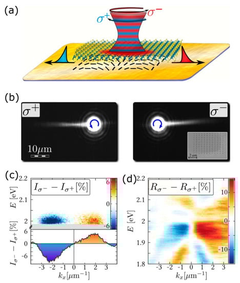
Figure 3.
(a) Chiral coupling of valley excitons in a 1L-TMDC with spin-momentum-locked surface plasmons on a surface with an array with -rotated rectangular apertures [21]. (b) Real-space leakage radiation microscope images of the surface plasmons launched by and excitations. (c) Differential PL dispersion spectrum for left and right circularly polarized excitations. The shaded regions in all panels are removed by the laser line filter, and the cross-cuts are taken at 2 eV. (d) Differential angle-resolved reflection spectrum for left and right circularly polarized light.
Another realization of a metasurface for valley-exciton sorting and routing in 1L-MoS2 was proposed in Reference [24]. The metasurface consists of asymmetrically shaped grooves on a silver (Ag) film arranged in a sub-wavelength period, Figure 4a. The SEM image of the cross-section of the realized asymmetric grooves is shown in Figure 4b. The spatial separation of valley excitons of opposite chirality is enabled by coupling to surface plasmon polaritons (SPPs) propagating along the asymmetrically shaped grooves. The operation principles of this approach are described below. As already mentioned, the +K and −K valley excitons in 1L-TMDCs can be modeled as in-plane circularly polarized dipoles oscillating with opposite helicity. However, the in-plane-oriented dipoles cannot asymmetrically excite conventional SPPs in a metasurface with symmetrically shaped grooves. Moreover, the efficiency of in-plane dipoles coupling to TM polarized SPPs is very small. These challenges require metasurfaces with asymmetric grooves, where the effective coupling between 1L-TMDC excitons and SPP waves is possible on the side walls. This crucial concept extends the photonic spin Hall effect to planar metasurfaces with only an in-plane electric field, and it enables chirality-dependent coupling between TMDs and metasurfaces. Figure 4c shows the experimentally observed degree of the valley-polarization (left) pattern over the metasurface. These results demonstrate the asymmetry of the measured PL signal from 1L-MoS2 on metasurfaces away from the laser excitation spot. The right plot shows the results from 1L-MoS2 on an Ag homogeneous substrate, where a vanishing degree of valley polarization is observed. A valley-exciton dividing of ~2 µm is demonstrated. Figure 4d demonstrates a line profile, , measured (left) and simulated (right) along the groove. The black dashed curve shows the fitting by subtracting two Gaussian curves.
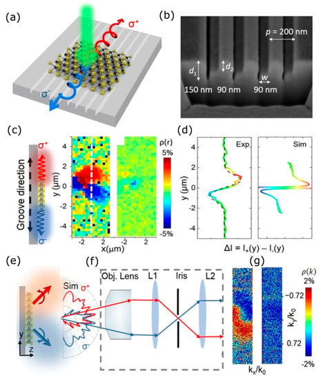
Figure 4.
Routing valley excitons in 1L-MoS2 with a metasurface made of monocrystalline silver (Ag) [24]. (a) Illustration of valley excitons in a monolayer TMD controlled by a metasurface consisting of asymmetric grooves. Not only are valley-polarized excitons spatially separated, but photons with opposite helicity are also emitted in different directions, serving as a valley–photon interface mediated by excitons. (b) SEM image of the cross-section of the asymmetric grooves. (c) Illustration of valley-exciton separation caused by the metasurface. Real-space color plot of valley polarization obtained from the (left) MoS2 metasurface and (right) MoS2 flat silver film under 532-nm laser excitation. (d) A line profile, , along the groove. The black dash curve is a fitting by subtracting two Gaussian curves (left). A line profile from the simulation (right). (e) Illustration of the helicity-dependent directional emission of the valley excitons (left). Numerically simulated far-field emission pattern from valley excitons with opposite helicity (right). (f) Set-up for the K-space mapping of PL. (g) Experimental distribution in photon momentum space obtained from (left) the MoS2 metasurface and (right) the MoS2 flat silver film.
It was also demonstrated that the metasurface emits photons with opposite helicity in different directions, dividing the valley degree of freedom in the far-field pattern (Figure 4e). Numerical results (Figure 4e, right panel) show that the and polarized photons preferentially emit toward the upper and lower hemisphere, respectively. The experimental results of measurement of the valley degree of freedom in the K-space, obtained with the set-up sketched in Figure 4f, are summarized in Figure 4g. These results clearly show the ability of the metasurface to divide the +K and −K valley exciton emissions into different radiation directions.
Concluding this section, we note that the proposed solutions for separating valley index are rather general, and they can be applied to a wide range of layered materials. Moreover, no exciton valley polarization is required, as is the case for MoS2 at room temperature, which allows utilizing this approach in valleytronics applications at room temperature.
4. Conclusions
In this paper, we reviewed state-of-the-art advances in 1L-TMDC valley degree-of-freedom separation, accompanied by valley-selective directional emission or real exciton dividing, mediated by resonant plasmonic nanostructures and nanoantennas. These works are aimed at overcoming a significant obstacle in the field of valleytronics related to short valley depolarization times and relatively short exciton lifetimes at room temperature, which prevent using valley pseudospin in on-chip integrated valley devices. The observed nanostructures for valley-selective directional emission allow either the spatial separation of the valley degree of freedom with surface waves, or separation in K-space when photons with opposite helicity are emitted in different directions. The existing works show that spatial separation of the valley degree of freedom may be accompanied by real dividing of valley excitons in space, or a transformation of valley exciton pseudospin into a photonic degree of freedom (e.g., transverse optical spin angular momentum) via optical spin–orbit coupling (or both these processes). This analysis was supported by a brief review of the optical properties of 2D TMDC materials, with attention paid to their photoluminescence/absorption spectra, dynamics of valley depolarization, and the valley Hall effect.
Author Contributions
Conceptualization, A.K. Funding acquisition, A.A. Supervision, A.A. Writing—original draft, A.K. Writing—review and editing, A.A.
Funding
This work was supported by the Air Force Office of Scientific Research and the Welch Foundation with grant No. F-1802.
Conflicts of Interest
The authors declare no conflicts of interest.
References
- Kish, L.B. End of Moore’s law: Thermal (noise) death of integration in micro and nano electronics. Phys. Lett. A 2002, 305, 144–149. [Google Scholar] [CrossRef]
- Joensen, P.; Frindt, R.F.; Morrison, S.R. Single-layer MoS2. Mater. Res. Bull. 1986, 21, 457–461. [Google Scholar] [CrossRef]
- Butler, S.Z.; Hollen, S.M.; Cao, L.; Cui, Y.; Gupta, J.A.; Gutiérrez, H.R.; Heinz, T.F.; Hong, S.S.; Huang, J.; Ismach, A.F.; et al. Progress, challenges, and opportunities in two-dimensional materials beyond graphene. ACS Nano 2013, 7, 2898–2926. [Google Scholar] [CrossRef] [PubMed]
- Xia, F.; Wang, H.; Xiao, D.; Dubey, M.; Ramasubramaniam, A. Two-dimensional material nanophotonics. Nat. Photonics 2014, 8, 899–907. [Google Scholar] [CrossRef]
- Mak, K.F.; Shan, J. Photonics and optoelectronics of 2D semiconductor transition metal dichalcogenides. Nat. Photonics 2016, 10, 216–226. [Google Scholar] [CrossRef]
- Bhimanapati, G.R.; Lin, Z.; Meunier, V.; Jung, Y.; Cha, J.; Das, S.; Xiao, D.; Son, Y.; Strano, M.S.; Cooper, V.R.; et al. Recent Advances in Two-Dimensional Materials beyond Graphene. ACS Nano 2015, 9, 11509–11539. [Google Scholar] [CrossRef] [PubMed]
- Das, S.; Robinson, J.A.; Dubey, M.; Terrones, H.; Terrones, M. Beyond Graphene: Progress in Novel Two-Dimensional Materials and van der Waals Solids. Annu. Rev. Mater. Res. 2015, 45, 1–27. [Google Scholar] [CrossRef]
- Grosso, G. 2D materials: Valley polaritons. Nat. Photonics 2017, 11, 455–456. [Google Scholar] [CrossRef]
- Schaibley, J.R.; Yu, H.; Clark, G.; Rivera, P.; Ross, J.S.; Seyler, K.L.; Yao, W.; Xu, X. Valleytronics in 2D materials. Nat. Rev. Mater. 2016, 1, 16055. [Google Scholar] [CrossRef]
- Manzeli, S.; Ovchinnikov, D.; Pasquier, D.; Yazyev, O.V.; Kis, A. 2D transition metal dichalcogenides. Nat. Rev. Mater. 2017, 2, 17033. [Google Scholar] [CrossRef]
- Koperski, M.; Molas, M.R.; Arora, A.; Nogajewski, K.; Slobodeniuk, A.O.; Faugeras, C.; Potemski, M. Optical properties of atomically thin transition metal dichalcogenides: Observations and puzzles. Nanophotonics 2017, 6, 1–20. [Google Scholar] [CrossRef]
- Krasnok, A.; Lepeshov, S.; Alú, A. Nanophotonics with 2D transition metal dichalcogenides [Invited]. Opt. Express 2018, 26, 15972. [Google Scholar] [CrossRef]
- Pu, J.; Takenobu, T. Monolayer Transition Metal Dichalcogenides as Light Sources. Adv. Mater. 2018, 1707627, 1–22. [Google Scholar] [CrossRef] [PubMed]
- Pospischil, A.; Mueller, T. Optoelectronic Devices Based on Atomically Thin Transition Metal Dichalcogenides. Appl. Sci. 2016, 6, 78. [Google Scholar] [CrossRef]
- Mak, K.F.; He, K.; Shan, J.; Heinz, T.F. Control of valley polarization in monolayer MoS2 by optical helicity. Nat. Nanotechnol. 2012, 7, 494–498. [Google Scholar] [CrossRef] [PubMed]
- Zeng, H.; Dai, J.; Yao, W.; Xiao, D.; Cui, X. Valley polarization in MoS2 monolayers by optical pumping. Nat. Nanotechnol. 2012, 7, 490–493. [Google Scholar] [CrossRef] [PubMed]
- Cao, T.; Wang, G.; Han, W.; Ye, H.; Zhu, C.; Shi, J.; Niu, Q.; Tan, P.; Wang, E.; Liu, B.; et al. Valley-selective circular dichroism of monolayer molybdenum disulphide. Nat. Commun. 2012, 3, 885–887. [Google Scholar] [CrossRef] [PubMed]
- Gunawan, O.; Shkolnikov, Y.P.; Vakili, K.; Gokmen, T.; De Poortere, E.P.; Shayegan, M. Valley Susceptibility of an Interacting Two-Dimensional Electron System. Phys. Rev. Lett. 2006, 97, 186404. [Google Scholar] [CrossRef] [PubMed]
- Xu, X.; Yao, W.; Xiao, D.; Heinz, T.F. Spin and pseudospins in layered transition metal dichalcogenides. Nat. Phys. 2014, 10, 343–350. [Google Scholar] [CrossRef]
- Xiao, D.; Liu, G.B.; Feng, W.; Xu, X.; Yao, W. Coupled Spin and Valley Physics in Monolayers of MoS2 and Other Group-VI Dichalcogenides. Phys. Rev. Lett. 2012, 108, 196802. [Google Scholar] [CrossRef] [PubMed]
- Chervy, T.; Azzini, S.; Lorchat, E.; Wang, S.; Gorodetski, Y.; Hutchison, J.A.; Berciaud, S.; Ebbesen, T.W.; Genet, C. Room Temperature Chiral Coupling of Valley Excitons with Spin-Momentum Locked Surface Plasmons. ACS Photonics 2018, 5, 1281–1287. [Google Scholar] [CrossRef]
- Chen, H.; Liu, M.; Xu, L.; Neshev, D.N. Valley-selective directional emission from a transition-metal dichalcogenide monolayer mediated by a plasmonic nanoantenna. Beilstein J. Nanotechnol. 2018, 9, 780–788. [Google Scholar] [CrossRef] [PubMed]
- Gong, S.H.; Alpeggiani, F.; Sciacca, B.; Garnett, E.C.; Kuipers, L. Nanoscale chiral valley-photon interface through optical spin-orbit coupling. Science 2018, 359, 443–447. [Google Scholar] [CrossRef] [PubMed]
- Sun, L.; Wang, C.; Krasnok, A.; Choi, J.; Shi, J.; Gomez-Diaz, J.S.; Zepeda, A.; Gwo, S.; Shih, C.; Andrea, A.; et al. Routing Valley Excitons in a Monolayer MoS2 with a Metasurface. arXiv, 2018; arXiv:1801.06543. [Google Scholar]
- Wang, Q.H.; Kalantar-Zadeh, K.; Kis, A.; Coleman, J.N.; Strano, M.S. Electronics and optoelectronics of two-dimensional transition metal dichalcogenides. Nat. Nanotechnol. 2012, 7, 699–712. [Google Scholar] [CrossRef] [PubMed]
- Choi, W.; Choudhary, N.; Han, G.H.; Park, J.; Akinwande, D.; Lee, Y.H. Recent development of two-dimensional transition metal dichalcogenides and their applications. Mater. Today 2017, 20, 116–130. [Google Scholar] [CrossRef]
- Jariwala, D.; Sangwan, V.K.; Lauhon, L.J.; Marks, T.J.; Hersam, M.C. Emerging device applications for semiconducting two-dimensional transition metal dichalcogenides. ACS Nano 2014, 8, 1102–1120. [Google Scholar] [CrossRef] [PubMed]
- Zhao, W.; Ghorannevis, Z.; Chu, L.; Toh, M.; Kloc, C.; Tan, P.-H.; Eda, G. Evolution of Electronic Structure in Atomically Thin Sheets of WS2 and WSe2. ACS Nano 2013, 7, 791–797. [Google Scholar] [CrossRef] [PubMed]
- Fang, H.; Bechtel, H.A.; Plis, E.; Martin, M.C.; Krishna, S.; Yablonovitch, E.; Javey, A. Quantum of optical absorption in two-dimensional semiconductors. Proc. Natl. Acad. Sci. USA 2013, 110, 11688–11691. [Google Scholar] [CrossRef] [PubMed]
- Wang, M.; Krasnok, A.; Zhang, T.; Scarabelli, L.; Liu, H.; Wu, Z.; Liz-Marzán, L.M.; Terrones, M.; Alù, A.; Zheng, Y. Tunable Fano Resonance and Plasmon-Exciton Coupling in Single Au Nanotriangles on Monolayer WS2 at Room Temperature. Adv. Mater. 2018, 30, 1705779. [Google Scholar] [CrossRef] [PubMed]
- Li, Y.; Chernikov, A.; Zhang, X.; Rigosi, A.; Hill, H.M.; van der Zande, A.M.; Chenet, D.A.; Shih, E.-M.; Hone, J.; Heinz, T.F. Measurement of the Optical Dielectric Function of Monolayer Transition-Metal Dichalcogenides: MoS2, MoSe2, WS2, and WSe2. Phys. Rev. B 2014, 90, 205422. [Google Scholar] [CrossRef]
- Ye, Z.; Cao, T.; O’Brien, K.; Zhu, H.; Yin, X.; Wang, Y.; Louie, S.G.; Zhang, X.; O’Brien, K.; Zhu, H.; et al. Probing excitonic dark states in single-layer tungsten disulphide. Nature 2014, 513, 214–218. [Google Scholar] [CrossRef] [PubMed]
- Ugeda, M.M.; Bradley, A.J.; Shi, S.-F.; da Jornada, F.H.; Zhang, Y.; Qiu, D.Y.; Ruan, W.; Mo, S.; Hussain, Z.; Shen, Z.; et al. Giant bandgap renormalization and excitonic effects in a monolayer transition metal dichalcogenide semiconductor. Nat. Mater. 2014, 13, 1091–1095. [Google Scholar] [CrossRef] [PubMed]
- Ross, J.S.; Wu, S.; Yu, H.; Ghimire, N.J.; Jones, A.M.; Aivazian, G.; Yan, J.; Mandrus, D.G.; Xiao, D.; Yao, W.; et al. Electrical control of neutral and charged excitons in a monolayer semiconductor. Nat. Commun. 2013, 4, 1473–1476. [Google Scholar] [CrossRef] [PubMed]
- Cuadra, J.; Baranov, D.G.; Wersäll, M.; Verre, R.; Antosiewicz, T.J.; Shegai, T. Observation of Tunable Charged Exciton Polaritons in Hybrid Monolayer WS2−Plasmonic Nanoantenna System. Nano Lett. 2018, 18, 1777–1785. [Google Scholar] [CrossRef] [PubMed]
- Shang, J.; Shen, X.; Cong, C.; Peimyoo, N.; Cao, B.; Eginligil, M.; Yu, T. Observation of excitonic fine structure in a 2D transition-metal dichalcogenide semiconductor. ACS Nano 2015, 9, 647–655. [Google Scholar] [CrossRef] [PubMed]
- Sie, E.J.; Lui, C.H.; Lee, Y.H.; Kong, J.; Gedik, N. Observation of Intervalley Biexcitonic Optical Stark Effect in Monolayer WS2. Nano Lett. 2016, 16, 7421–7426. [Google Scholar] [CrossRef] [PubMed]
- You, Y.; Zhang, X.X.; Berkelbach, T.C.; Hybertsen, M.S.; Reichman, D.R.; Heinz, T.F. Observation of biexcitons in monolayer WSe2. Nat. Phys. 2015, 11, 477–481. [Google Scholar] [CrossRef]
- Hao, K.; Specht, J.F.; Nagler, P.; Xu, L.; Tran, K.; Singh, A.; Dass, C.K.; Schüller, C.; Korn, T.; Richter, M.; et al. Neutral and charged inter-valley biexcitons in monolayer MoSe2. Nat. Commun. 2017, 8, 15552. [Google Scholar] [CrossRef] [PubMed]
- Kim, M.S.; Yun, S.J.; Lee, Y.; Seo, C.; Han, G.H.; Kim, K.K.; Lee, Y.H.; Kim, J. Biexciton Emission from Edges and Grain Boundaries of Triangular WS2 Monolayers. ACS Nano 2016, 10, 2399–2405. [Google Scholar] [CrossRef] [PubMed]
- Plechinger, G.; Korn, T.; Lupton, J.M. Valley-Polarized Exciton Dynamics in Exfoliated Monolayer WSe2. J. Phys. Chem. C 2017, 121, 6409–6413. [Google Scholar] [CrossRef]
- Park, K.-D.; Jiang, T.; Clark, G.; Xu, X.; Raschke, M.B. Radiative control of dark excitons at room temperature by nano-optical antenna-tip Purcell effect. Nat. Nanotechnol. 2017, 1–7. [Google Scholar] [CrossRef] [PubMed]
- Lopez-Sanchez, O.; Lembke, D.; Kayci, M.; Radenovic, A.; Kis, A. Ultrasensitive photodetectors based on monolayer MoS2. Nat. Nanotechnol. 2013, 8, 497–501. [Google Scholar] [CrossRef] [PubMed]
- Britnell, L.; Ribeiro, R.M.; Eckmann, A.; Jalil, R.; Belle, B.D.; Mishchenko, A.; Kim, Y.-J.; Gorbachev, R.V.; Georgiou, T.; Morozov, S.V.; et al. Strong Light-Matter Interactions in Heterostructures of Atomically Thin Films. Science 2013, 340, 1311–1314. [Google Scholar] [CrossRef] [PubMed]
- Perea-Lõpez, N.; Elías, A.L.; Berkdemir, A.; Castro-Beltran, A.; Gutiérrez, H.R.; Feng, S.; Lv, R.; Hayashi, T.; Lõpez-Urías, F.; Ghosh, S.; et al. Photosensor device based on few-layered WS2 films. Adv. Funct. Mater. 2013, 23, 5511–5517. [Google Scholar] [CrossRef]
- Koppens, F.H.L.; Mueller, T.; Avouris, P.; Ferrari, A.C.; Vitiello, M.S.; Polini, M. Photodetectors based on graphene, other two-dimensional materials and hybrid systems. Nat. Nanotechnol. 2014, 9, 780–793. [Google Scholar] [CrossRef] [PubMed]
- Yin, Z.; Li, H.; Li, H.; Jiang, L.; Shi, Y.; Sun, Y.; Lu, G.; Zhang, Q.; Chen, X.; Zhang, H. Single-Layer MoS2 Phototransistors. ACS Nano 2012, 6, 74–80. [Google Scholar] [CrossRef] [PubMed]
- Sun, Z.; Martinez, A.; Wang, F. Optical modulators with 2D layered materials. Nat. Photonics 2016, 10, 227–238. [Google Scholar] [CrossRef]
- Lopez-Sanchez, O.; Alarcon Llado, E.; Koman, V.; Fontcuberta I Morral, A.; Radenovic, A.; Kis, A. Light generation and harvesting in a van der waals heterostructure. ACS Nano 2014, 8, 3042–3048. [Google Scholar] [CrossRef] [PubMed]
- Withers, F.; Del Pozo-Zamudio, O.; Mishchenko, A.; Rooney, A.P.; Gholinia, A.; Watanabe, K.; Taniguchi, T.; Haigh, S.J.; Geim, A.K.; Tartakovskii, A.I.; et al. Light-emitting diodes by band-structure engineering in van der Waals heterostructures. Nat. Mater. 2015, 14, 301–306. [Google Scholar] [CrossRef] [PubMed]
- Liu, C.H.; Clark, G.; Fryett, T.; Wu, S.; Zheng, J.; Hatami, F.; Xu, X.; Majumdar, A. Nanocavity integrated van der Waals heterostructure light-emitting tunneling diode. Nano Lett. 2017, 17, 200–205. [Google Scholar] [CrossRef] [PubMed]
- He, Y.-M.; Clark, G.; Schaibley, J.R.; He, Y.; Chen, M.-C.; Wei, Y.-J.; Ding, X.; Zhang, Q.; Yao, W.; Xu, X.; et al. Single quantum emitters in monolayer semiconductors. Nat. Nanotechnol. 2015, 10, 497–502. [Google Scholar] [CrossRef] [PubMed]
- Tonndorf, P.; Schmidt, R.; Schneider, R.; Kern, J.; Buscema, M.; Steele, G.A.; Castellanos-Gomez, A.; van der Zant, H.S.J.; Michaelis de Vasconcellos, S.; Bratschitsch, R. Single-photon emission from localized excitons in an atomically thin semiconductor. Optica 2015, 2, 347. [Google Scholar] [CrossRef]
- Amani, M.; Lien, D.H.; Kiriya, D.; Xiao, J.; Azcatl, A.; Noh, J.; Madhvapathy, S.R.; Addou, R.; Santosh, K.C.; Dubey, M.; et al. Near-unity photoluminescence quantum yield in MoS2. Science 2015, 350, 1065–1068. [Google Scholar] [CrossRef] [PubMed]
- Amani, M.; Taheri, P.; Addou, R.; Ahn, G.H.; Kiriya, D.; Lien, D.H.; Ager, J.W.; Wallace, R.M.; Javey, A. Recombination Kinetics and Effects of Superacid Treatment in Sulfur- and Selenium-Based Transition Metal Dichalcogenides. Nano Lett. 2016, 16, 2786–2791. [Google Scholar] [CrossRef] [PubMed]
- Johnson, A.D.; Cheng, F.; Tsai, Y.; Shih, C.K. Giant Enhancement of Defect-Bound Exciton Luminescence and Suppression of Band-Edge Luminescence in Monolayer WSe2-Ag Plasmonic Hybrid Structures. Nano Lett. 2017, 17, 4317–4322. [Google Scholar] [CrossRef] [PubMed]
- Zheng, D.; Zhang, S.; Deng, Q.; Kang, M.; Nordlander, P.; Xu, H. Manipulating coherent plasmon-exciton interaction in a single silver nanorod on monolayer WSe2. Nano Lett. 2017, 17, 3809–3814. [Google Scholar] [CrossRef] [PubMed]
- Huang, J.; Akselrod, G.M.; Ming, T.; Kong, J.; Mikkelsen, M.H. Tailored Emission Spectrum of 2D Semiconductors Using Plasmonic Nanocavities. ACS Photonics 2018, 5, 552–558. [Google Scholar] [CrossRef]
- Eda, G.; Maier, S.A. Two-dimensional crystals: Managing light for optoelectronics. ACS Nano 2013, 7, 5660–5665. [Google Scholar] [CrossRef] [PubMed]
- Akselrod, G.M.; Ming, T.; Argyropoulos, C.; Hoang, T.B.; Lin, Y.; Ling, X.; Smith, D.R.; Kong, J.; Mikkelsen, M.H. Leveraging nanocavity harmonics for control of optical processes in 2d semiconductors. Nano Lett. 2015, 15, 3578–3584. [Google Scholar] [CrossRef] [PubMed]
- Tahersima, M.H.; Birowosuto, M.D.; Ma, Z.; Coley, W.C.; Valentin, M.D.; Naghibi Alvillar, S.; Lu, I.-H.; Zhou, Y.; Sarpkaya, I.; Martinez, A.; et al. Testbeds for Transition Metal Dichalcogenide Photonics: Efficacy of Light Emission Enhancement in Monomer vs Dimer Nanoscale Antennae. ACS Photonics 2017, 4, 1713–1721. [Google Scholar] [CrossRef]
- Noori, Y.J.; Cao, Y.; Roberts, J.; Woodhead, C.; Bernardo-Gavito, R.; Tovee, P.; Young, R.J. Photonic Crystals for Enhanced Light Extraction from 2D Materials. ACS Photonics 2016, 3, 2515–2520. [Google Scholar] [CrossRef]
- Galfsky, T.; Sun, Z.; Considine, C.R.C.R.; Chou, C.-T.T.; Ko, W.-C.C.; Lee, Y.-H.H.; Narimanov, E.E.; Menon, V.M. Broadband Enhancement of Spontaneous Emission in Two-Dimensional Semiconductors Using Photonic Hypercrystals. Nano Lett. 2016, 16, 4940–4945. [Google Scholar] [CrossRef] [PubMed]
- Wen, J.; Wang, H.; Wang, W.; Deng, Z.; Zhuang, C.; Zhang, Y.; Liu, F.; She, J.; Chen, J.; Chen, H.; et al. Room-Temperature Strong Light–Matter Interaction with Active Control in Single Plasmonic Nanorod Coupled with Two-Dimensional Atomic Crystals. Nano Lett. 2017, 17, 4689–4697. [Google Scholar] [CrossRef] [PubMed]
- Li, Z.; Li, Y.; Han, T.; Wang, X.; Yu, Y.; Tay, B.; Liu, Z.; Fang, Z. Tailoring MoS2 Exciton-Plasmon Interaction by Optical Spin-Orbit Coupling. ACS Nano 2017, 11, 1165–1171. [Google Scholar] [CrossRef] [PubMed]
- Abid, I.; Chen, W.; Yuan, J.; Bohloul, A.; Najmaei, S.; Avendano, C.; Péchou, R.; Mlayah, A.; Lou, J. Temperature-Dependent Plasmon–Exciton Interactions in Hybrid Au/MoSe2 Nanostructures. ACS Photonics 2017, 4, 1653–1660. [Google Scholar] [CrossRef]
- Sigle, D.O.; Mertens, J.; Herrmann, L.O.; Bowman, R.W.; Ithurria, S.; Dubertret, B.; Shi, Y.; Yang, H.Y.; Tserkezis, C.; Aizpurua, J.; et al. Monitoring morphological changes in 2D monolayer semiconductors using atom-thick plasmonic nanocavities. ACS Nano 2015, 9, 825–830. [Google Scholar] [CrossRef] [PubMed]
- Zhang, X.; Choi, S.; Wang, D.; Naylor, C.H.; Johnson, A.T.C.; Cubukcu, E. Unidirectional Doubly Enhanced MoS2 Emission via Photonic Fano Resonances. Nano Lett. 2017, 17. [Google Scholar] [CrossRef] [PubMed]
- Lee, M.-G.; Yoo, S.; Kim, T.; Park, Q.-H. Large-area plasmon enhanced two-dimensional MoS2. Nanoscale 2017, 9, 16244–16248. [Google Scholar] [CrossRef] [PubMed]
- Gonçalves, P.A.D.; Bertelsen, L.P.; Xiao, S.; Mortensen, N.A. Plasmon-exciton polaritons in two-dimensional semiconductor/metal interfaces. Phys. Rev. B 2018, 97, 41402. [Google Scholar] [CrossRef]
- Wang, S.; Li, S.; Chervy, T.; Shalabney, A.; Azzini, S.; Orgiu, E.; Hutchison, J.A.; Genet, C.; Samorì, P.; Ebbesen, T.W. Coherent coupling of WS2 monolayers with metallic photonic nanostructures at room temperature. Nano Lett. 2016, 16, 4368–4374. [Google Scholar] [CrossRef] [PubMed]
- Baranov, D.G.; Wersäll, M.; Cuadra, J.; Antosiewicz, T.J.; Shegai, T. Novel Nanostructures and Materials for Strong Light–Matter Interactions. ACS Photonics 2017, 5. [Google Scholar] [CrossRef]
- Wang, M.; Li, W.; Scarabelli, L.; Rajeeva, B.B.; Terrones, M.; Liz-Marzán, L.M.; Akinwande, D.; Zheng, Y. Plasmon–trion and plasmon–exciton resonance energy transfer from a single plasmonic nanoparticle to monolayer MoS2. Nanoscale 2017, 9, 13947–13955. [Google Scholar] [CrossRef] [PubMed]
- Jones, A.M.; Yu, H.; Ghimire, N.J.; Wu, S.; Aivazian, G.; Ross, J.S.; Zhao, B.; Yan, J.; Mandrus, D.G.; Xiao, D.; et al. Optical generation of excitonic valley coherence in monolayer WSe2. Nat. Nanotechnol. 2013, 8, 634–638. [Google Scholar] [CrossRef] [PubMed]
- Mak, K.F.; McGill, K.L.; Park, J.; McEuen, P.L. The valley hall effect in MoS2 transistors. Science 2014, 344, 1489–1492. [Google Scholar] [CrossRef] [PubMed]
- Lagarde, D.; Bouet, L.; Marie, X.; Zhu, C.R.; Liu, B.L.; Amand, T.; Tan, P.H.; Urbaszek, B. Carrier and Polarization Dynamics in Monolayer MoS2. Phys. Rev. Lett. 2014, 112, 47401. [Google Scholar] [CrossRef] [PubMed]
- Onga, M.; Zhang, Y.; Ideue, T.; Iwasa, Y. Exciton Hall effect in monolayer MoS2. Nat. Mater. 2017, 16, 1193–1197. [Google Scholar] [CrossRef] [PubMed]
- Shin, D.; Hübener, H.; De Giovannini, U.; Jin, H.; Rubio, A.; Park, N. Phonon-driven spin-Floquet magneto-valleytronics in MoS2. Nat. Commun. 2018, 9, 638. [Google Scholar] [CrossRef] [PubMed]
- Zhu, C.R.; Zhang, K.; Glazov, M.; Urbaszek, B.; Amand, T.; Ji, Z.W.; Liu, B.L.; Marie, X. Exciton valley dynamics probed by Kerr rotation in WSe2 monolayers. Phys. Rev. B Condens. Matter Mater. Phys. 2014, 90, 1–5. [Google Scholar] [CrossRef]
- Plechinger, G.; Nagler, P.; Arora, A.; Schmidt, R.; Chernikov, A.; del Águila, A.G.; Christianen, P.C.M.; Bratschitsch, R.; Schüller, C.; Korn, T. Trion fine structure and coupled spin–valley dynamics in monolayer tungsten disulfide. Nat. Commun. 2016, 7, 12715. [Google Scholar] [CrossRef] [PubMed]
- Molina-Sánchez, A.; Sangalli, D.; Wirtz, L.; Marini, A. Ab Initio Calculations of Ultrashort Carrier Dynamics in Two-Dimensional Materials: Valley Depolarization in Single-Layer WSe2. Nano Lett. 2017, 17, 4549–4555. [Google Scholar] [CrossRef] [PubMed]
- Xiao, D.; Yao, W.; Niu, Q. Valley-Contrasting Physics in Graphene: Magnetic Moment and Topological Transport. Phys. Rev. Lett. 2007, 99, 236809. [Google Scholar] [CrossRef] [PubMed]
- Yao, W.; Xiao, D.; Niu, Q. Valley-dependent optoelectronics from inversion symmetry breaking. Phys. Rev. B 2008, 77, 235406. [Google Scholar] [CrossRef]
- Rivera, P.; Seyler, K.L.; Yu, H.; Schaibley, J.R.; Yan, J.; Mandrus, D.G.; Yao, W.; Xu, X. Valley-polarized exciton dynamics in a 2D semiconductor heterostructure. Science 2016, 351, 688–691. [Google Scholar] [CrossRef] [PubMed]
- Selig, M.; Berghäuser, G.; Raja, A.; Nagler, P.; Schüller, C.; Heinz, T.F.; Korn, T.; Chernikov, A.; Malic, E.; Knorr, A. Excitonic linewidth and coherence lifetime in monolayer transition metal dichalcogenides. Nat. Commun. 2016, 7. [Google Scholar] [CrossRef] [PubMed]
- Aharonovich, I.; Englund, D.; Toth, M. Solid-state single-photon emitters. Nat. Photonics 2016, 10, 631–641. [Google Scholar] [CrossRef]
- Steinleitner, P.; Merkl, P.; Nagler, P.; Mornhinweg, J.; Schüller, C.; Korn, T.; Chernikov, A.; Huber, R. Direct Observation of Ultrafast Exciton Formation in a Monolayer of WSe2. Nano Lett. 2017, 17, 1455–1460. [Google Scholar] [CrossRef] [PubMed]
- Glazov, M.M.; Amand, T.; Marie, X.; Lagarde, D.; Bouet, L.; Urbaszek, B. Exciton fine structure and spin decoherence in monolayers of transition metal dichalcogenides. Phys. Rev. B Condens. Matter Mater. Phys. 2014, 89, 1–5. [Google Scholar] [CrossRef]
- Petersen, J.; Volz, J.; Rauschenbeutel, A. Chiral nanophotonic waveguide interface based on spin-orbit interaction of light. Science 2014, 346, 67–71. [Google Scholar] [CrossRef] [PubMed]
- Rodriguez-Fortuno, F.J.; Marino, G.; Ginzburg, P.; O’Connor, D.; Martinez, A.; Wurtz, G.A.; Zayats, A.V. Near-Field Interference for the Unidirectional Excitation of Electromagnetic Guided Modes. Science 2013, 340, 328–330. [Google Scholar] [CrossRef] [PubMed]
- Li, S.V.; Baranov, D.G.; Krasnok, A.E.; Belov, P.A. All-dielectric nanoantennas for unidirectional excitation of electromagnetic guided modes. Appl. Phys. Lett. 2015, 107. [Google Scholar] [CrossRef]
- Lodahl, P.; Mahmoodian, S.; Stobbe, S.; Schneeweiss, P.; Volz, J.; Rauschenbeutel, A.; Pichler, H.; Zoller, P. Chiral Quantum Optics. Nature 2016, 541, 473–480. [Google Scholar] [CrossRef] [PubMed]
- Arora, A.; Koperski, M.; Nogajewski, K.; Marcus, J.; Faugeras, C.; Potemski, M. Excitonic resonances in thin films of WSe2: From monolayer to bulk material. Nanoscale 2015, 7, 10421–10429. [Google Scholar] [CrossRef] [PubMed]
- Krasnok, A.; Caldarola, M.; Bonod, N.; Alú, A. Spectroscopy and Biosensing with Optically Resonant Dielectric Nanostructures. Adv. Opt. Mater. 2018, 6, 1701094. [Google Scholar] [CrossRef]
© 2018 by the authors. Licensee MDPI, Basel, Switzerland. This article is an open access article distributed under the terms and conditions of the Creative Commons Attribution (CC BY) license (http://creativecommons.org/licenses/by/4.0/).