Article

Cavity Design in Woodpile Based 3D Photonic Crystals

Department of Electrical and Electronic Engineering, University of Bristol, Bristol, BS8 1US, UK
*
Authors to whom correspondence should be addressed.
Appl. Sci. 2018, 8(7), 1087; https://doi.org/10.3390/app8071087
Submission received: 25 May 2018 / Revised: 25 June 2018 / Accepted: 3 July 2018 / Published: 5 July 2018
(This article belongs to the Special Issue Novel Advances in Optical Micro- and Nano-Cavities)

Abstract

:
In this paper, we present a design of a three-dimensional (3D) photonic crystal (PhC) nanocavity based on an optimized woodpile structure. By carefully choosing the position of the defect at the lattice center, we can create a cavity with high symmetry which supports well confined Gaussian-like cavity modes similar to those seen in a Fabry Perot laser resonator. We could also tune the resonant frequency of the cavity and manually choose the cavity mode order by adjusting the size of the defect at a chosen position.

Graphical Abstract

1. Introduction

There has been significant interest in three-dimensional photonic crystal (3D PhC) structures in recent years aiming to exploit full photonic band gaps (PBG) [1,2,3] and the unprecedented confinement of light at defects in these structures. A variety of structures have shown complete photonic bandgaps including dielectric spheres in a face-centered-cubic (FCC) lattice [4,5,6], rod-connected diamond (RCD) structures [7,8], ‘Yablonovite’ PhC [9] and woodpile based PhC structure [10]. Various defects can be introduced in such perfect crystals to create localized photonic modes such as optical waveguides [11,12,13,14,15] and nanocavities [16,17,18,19,20,21,22]. Light trapped in such defects interacts strongly with light emitters making them suitable for ultra-low-threshold lasers [23,24,25,26], enhanced optoelectronic sensors [27,28,29,30], ultrafast and low-power all-optical switches [31,32,33,34] and quantum information processing devices with non-linearity at the single photon level [35,36,37,38]. Although much effort has been made in applications of 1D or 2D PhCs [39,40,41,42], they still lose the confinement of light in the third dimension but rely on a total internal reflection. This leads to out-of-plane losses and manufactural restrictions such as suspended membranes or low index substrates. In a 3D PhC structure, the cavity mode is strongly associated with the surrounding environment which could result in a rich variety of mode patterns. Recently, fabrication of 3D photonic structures by direct laser writing (DLW) using two-photon polymerization (TPP) [43] has been reported creating woodpile [44,45,46,47] and RCD structures [48]. Notably, the woodpile structure is a promising structure which could be possible to mass produce with lower cost methods via layer by layer 2D lithographic approaches [13,49]. Although current applications are rather limited by the challenges of fabrications, some pioneering work has been proposed and implemented for various applications such as photon guiding [13,49] and spontaneous-emission control [50].
In this study, we choose a woodpile structure formed by rectangular rods as the template. Design of the defect in such woodpile based 3D PhC structures is investigated through comparing the woodpile lattice with the RCD lattice [8]. Although a woodpile formed by rectangular rods may not hold the widest photonic bandgap record as an inverse woodpile [10] or a RCD structure does [6,7,8], such discussion about the position of a defect based on the lattice still could apply more generally to other kinds of structures [21]. We found that, by carefully choosing the position of the defect, we could create a cavity with high symmetry which supports well confined cavity modes and also demonstrate that such a cavity in a woodpile based 3D PhC structure works in a similar way to a Fabry Perot laser resonator [51]. Moreover, choosing the specific defect position can help to simplify the analysis of the mode pattern as a result of the combination of the cavity with and without the 3D PhC surroundings.
This paper is organized as follows. In Section 2, we introduce the simulation methods applied throughout this paper. We then detail the designed woodpile structure in Section 3 with optimized parameters used in our simulations and the position we choose for the cavity. The principle of choosing this position is also discussed. In Section 4, we show the numerical results to demonstrate the tunable cavity mode and mode volume.

2. Calculation Methods

We first use the plane-wave expansion (PWE) method [52] to calculate the band structure for the woodpile template without any defect in the frequency domain. This gives us the dispersion relation of the woodpile template and the position of the complete photonic bandgap. We then use our in-house three-dimensional finite-difference time-domain (FDTD) software [17,20,21,53] with perfectly-matched layer (PML) boundary and a non-homogeneous mesh of around 107 cells to implement each simulation when various defects are introduced into the woodpile template. A broadband dipole source and multiple field probes are placed inside the defect to excite and monitor the field decay over time. The resonant frequencies fc, linewidths ∆f and Q factors (defined as fc/∆f) are then estimated by analysing the field decay in the frequency domain via the fast Fourier transform (FFT) and the filter diagonalization method using the Harminv software [54]. Effective mode volumes are also calculated using the definition,
Veff = ∭ε(r)|E(r)|2 d3r/[ε(r)|E(r)|2]max,
where E(r) is the resonant field and ε(r) is the dielectric constant at position r. For each resonant mode, we take the integration of the mode energy through sufficient computational volume to ensure convergence.

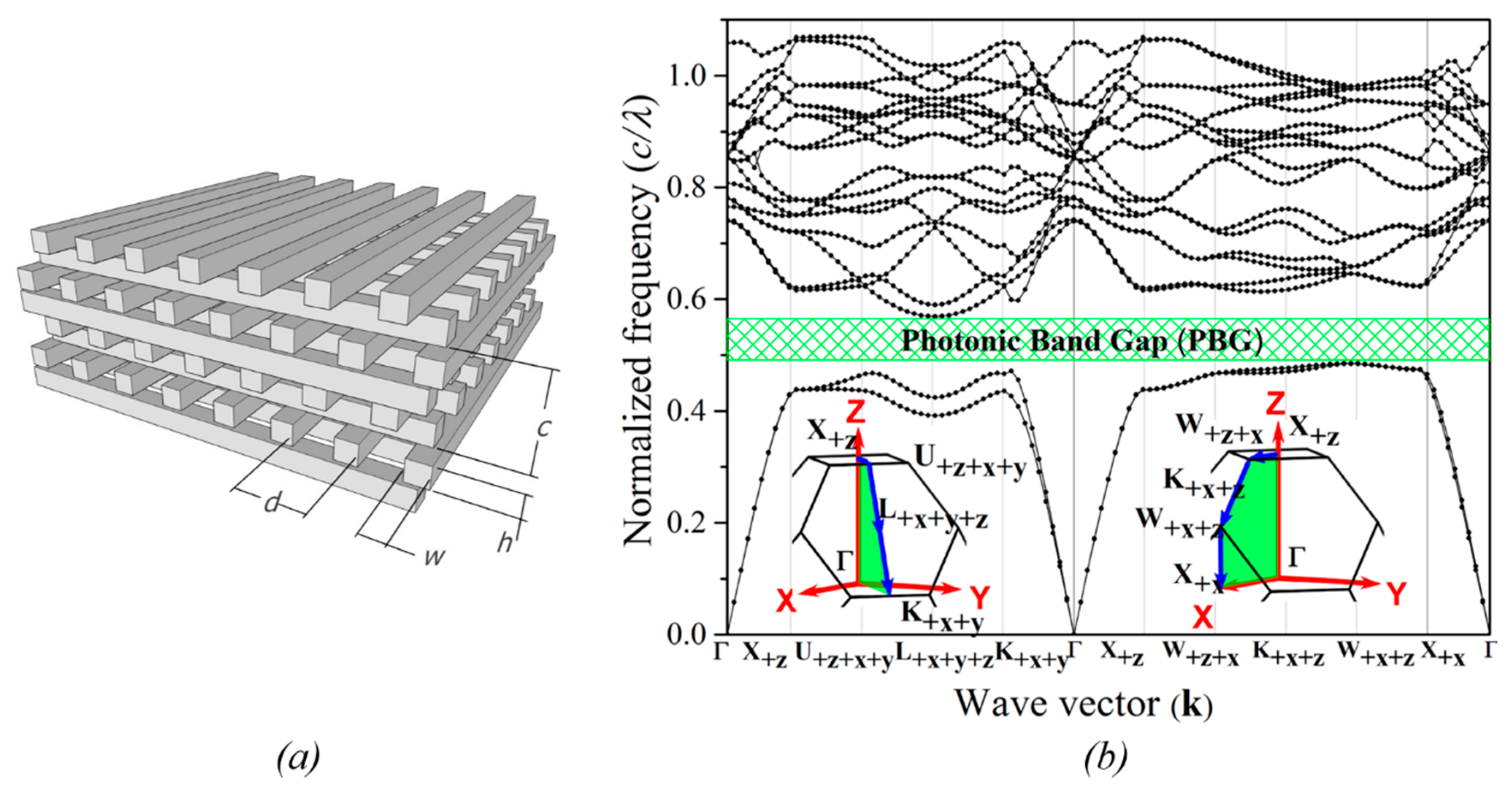
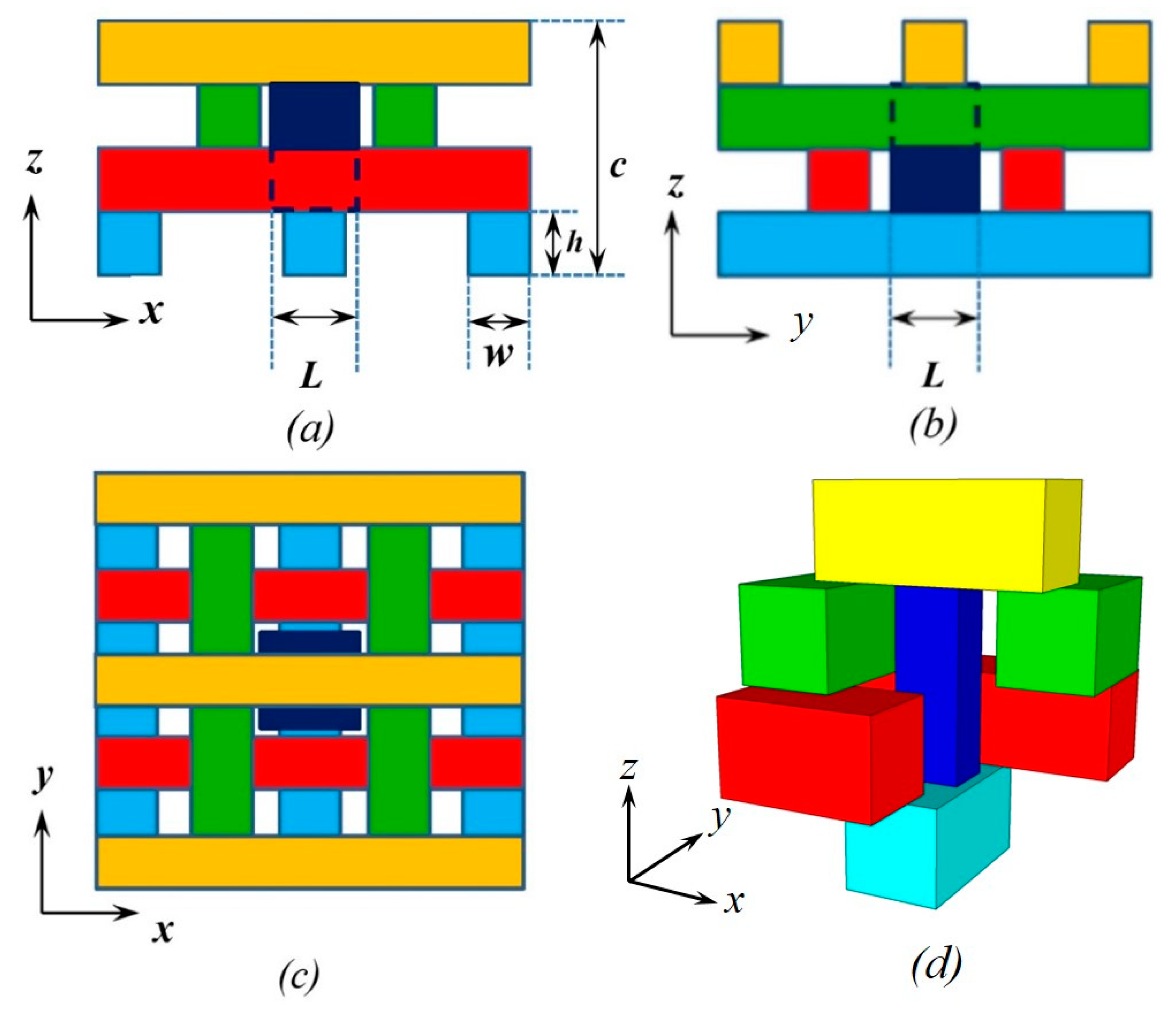
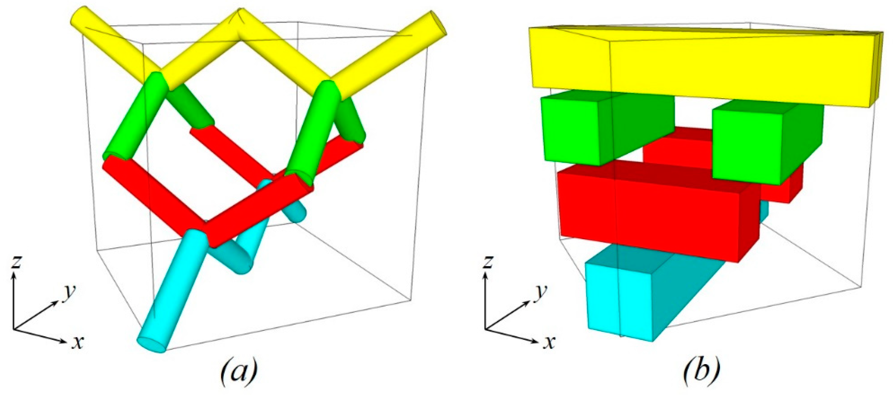
3. Woodpile Parameters and Cavity Design

In Figure 1a we show the woodpile structure we are modelling. The woodpile forms an FCC lattice when the height of the rods h is equal to c/4 [1], and the distance between two adjacent rods d = c/√2 where c indicates the vertical period which is also the height of four stacking layers. Before we show the numerical results and the defect design, we choose the optimized woodpile with widest complete photonic bandgap simply by adjusting the width w of the rods [20]. Throughout this work the refractive index of logs is nrod = 3.3, corresponding to common semiconductor materials such as Gallium Phosphide (GaP), while the background material is air nair = 1. Figure 1b shows the band structure calculated using plane-wave expansion (PWE) [52] method. The green region indicates the location of the optimized complete photonic bandgap which ranges from normalized frequency c/λ = 0.485 to 0.569 (where λ is the wavelength) and the gap/midgap ratio reaches a maximum value of 15.88% when the width of rods w = 0.21c [20]. All the simulations shown in this paper are based on this woodpile template with optimized parameter specified in Figure 1.
Since we have the optimized woodpile, we start to introduce a rectangular parallelepiped defect to create a cavity. The whole simulated woodpile template has 37 stacking layers in the z direction and 13 rods in each layer. The location of the defect is placed between the 19th layer and the 20th layer counting from the bottom. The refractive index of the defect is the same as that of the rods ndefect = 3.3 in this paper. Figure 2 shows the location of the defect in one vertical period (four stacking layers in z axis). The defect is placed between the middle layers and the height of the defect is 2h which makes it connect with both rods in the upper and lower layer. In both middle layers, the center of defect is also between two adjacent rods.
Woodpile is face-center-cubic (FCC) structure, which could be considered as a rod-connected diamond lattice. As shown in Figure 3, rods in different colors in rod-connected diamond lattice (a) stand for different layers in woodpile lattice (b) [8]. The woodpile structure is obtained by substituting short rods in rod-connected diamond lattice with a single long rod. The position of defects shown in this paper is thus chosen from the body center of the lattice to get the most symmetrical position.

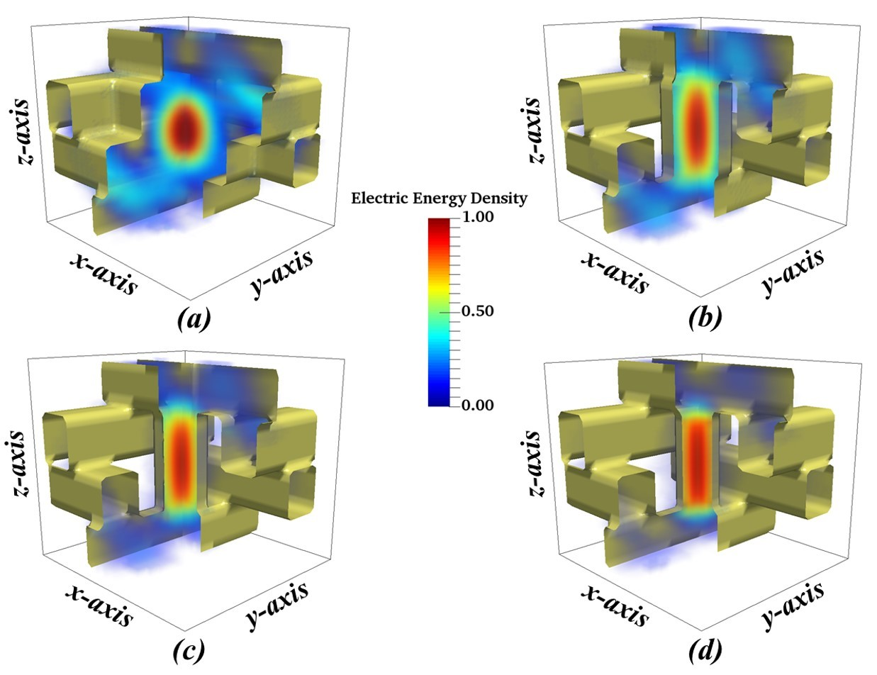
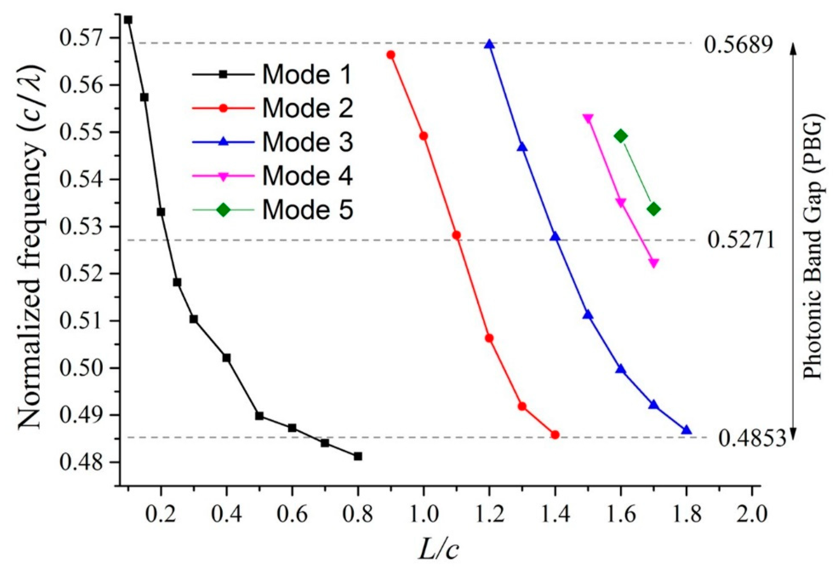
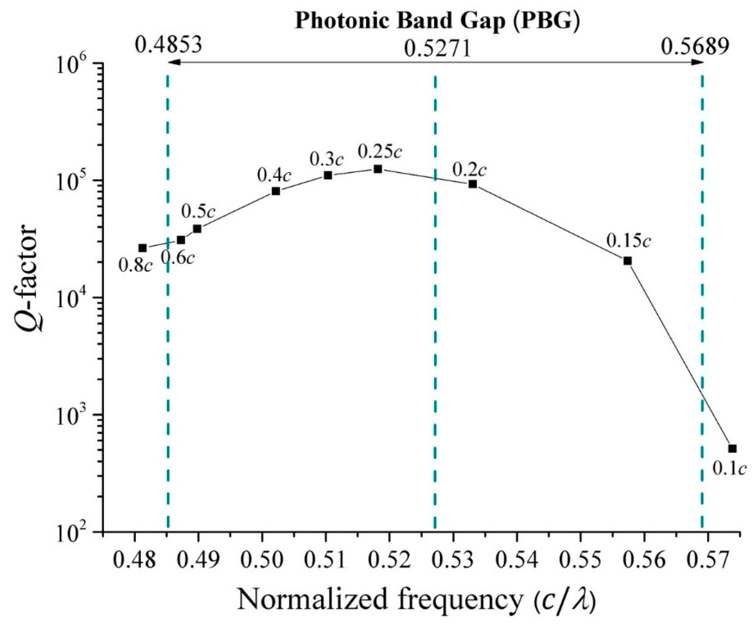
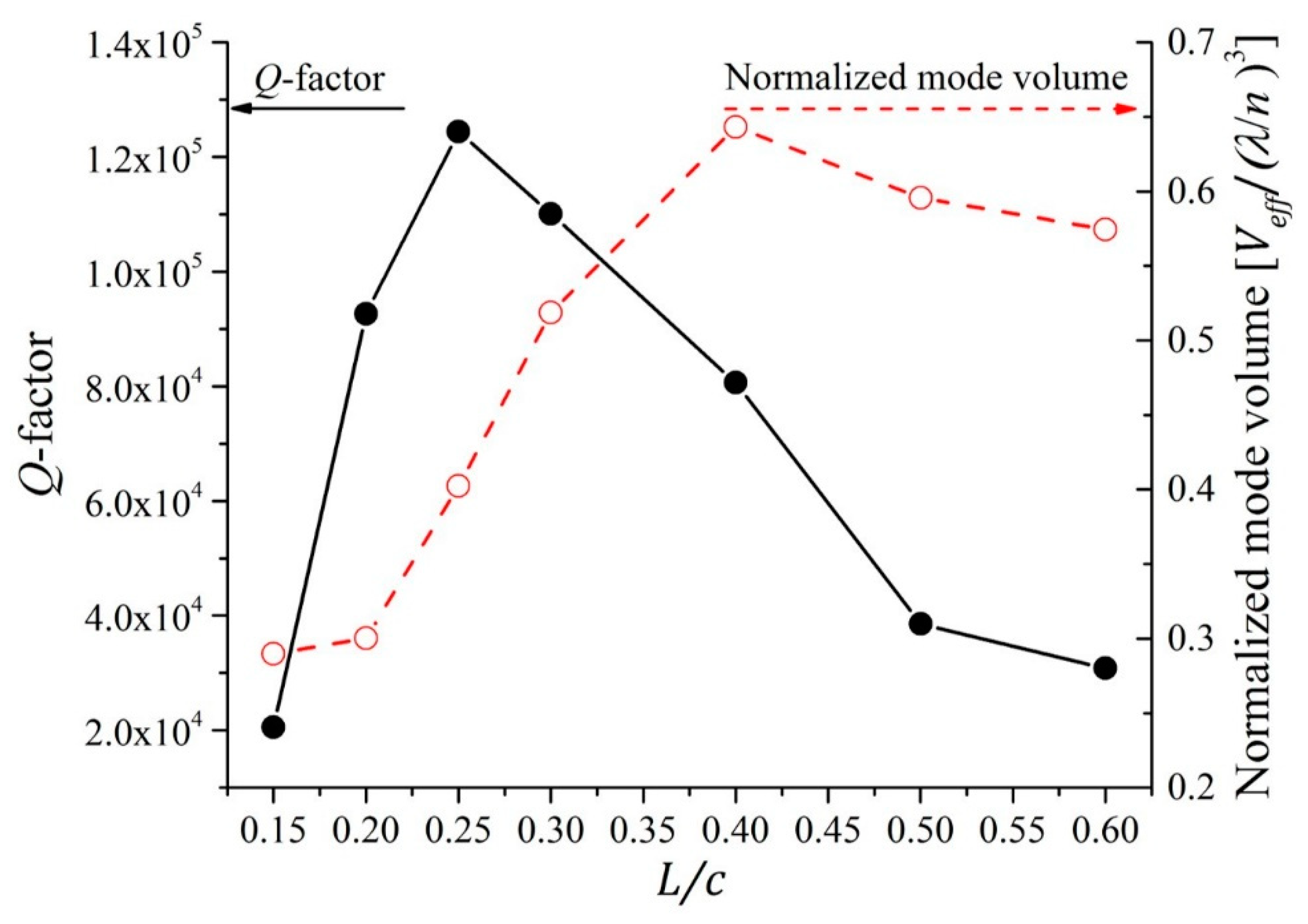
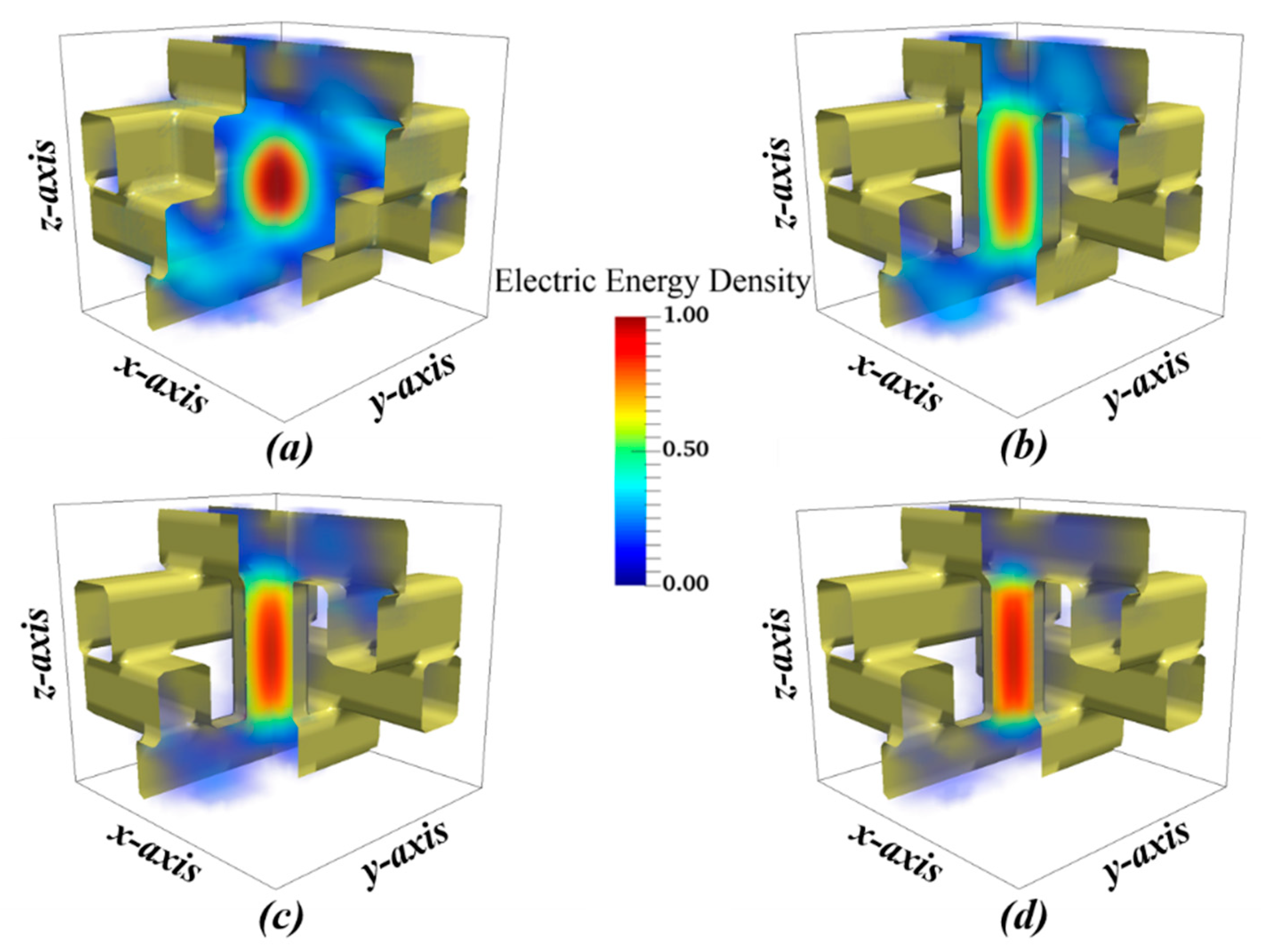
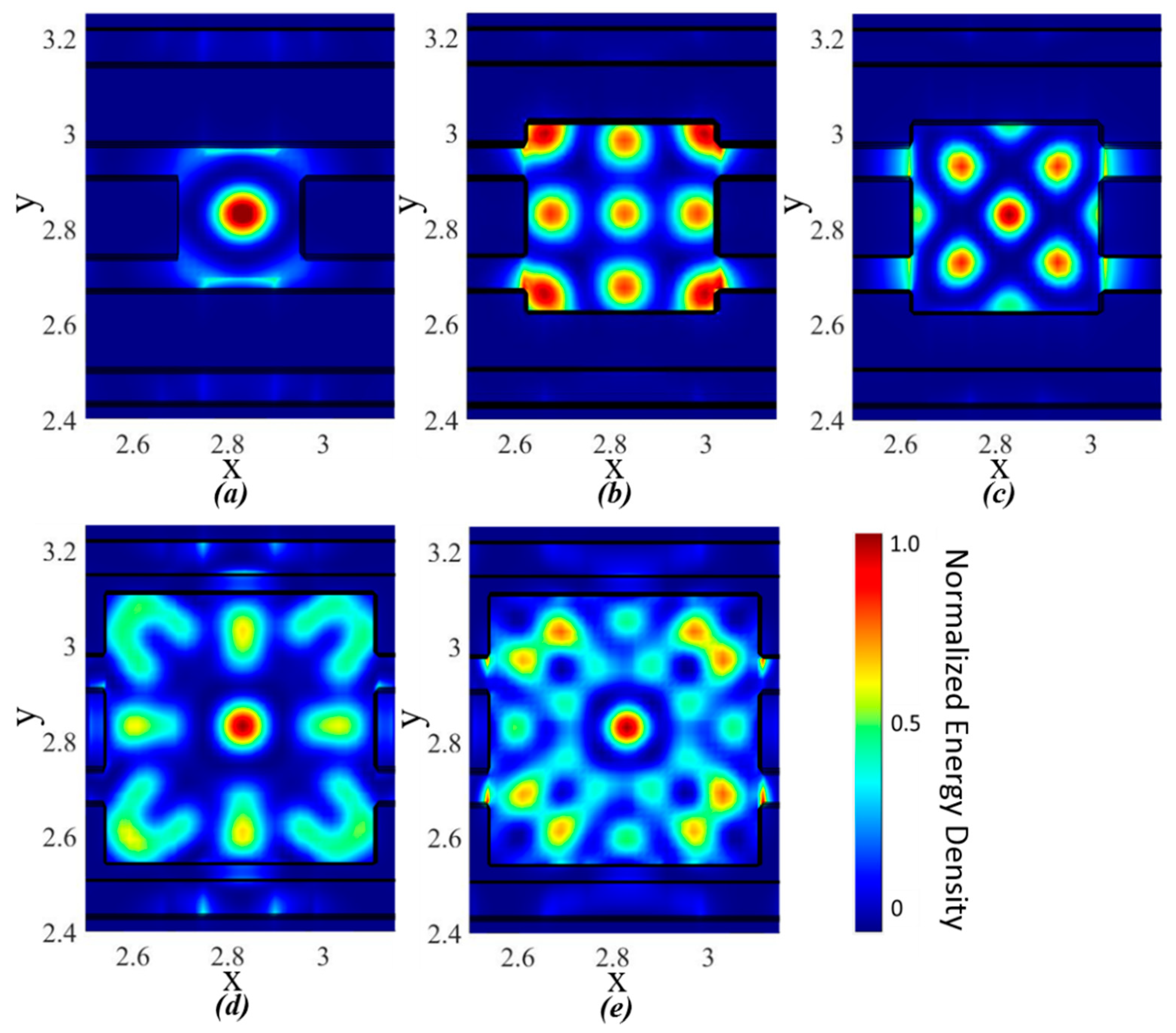
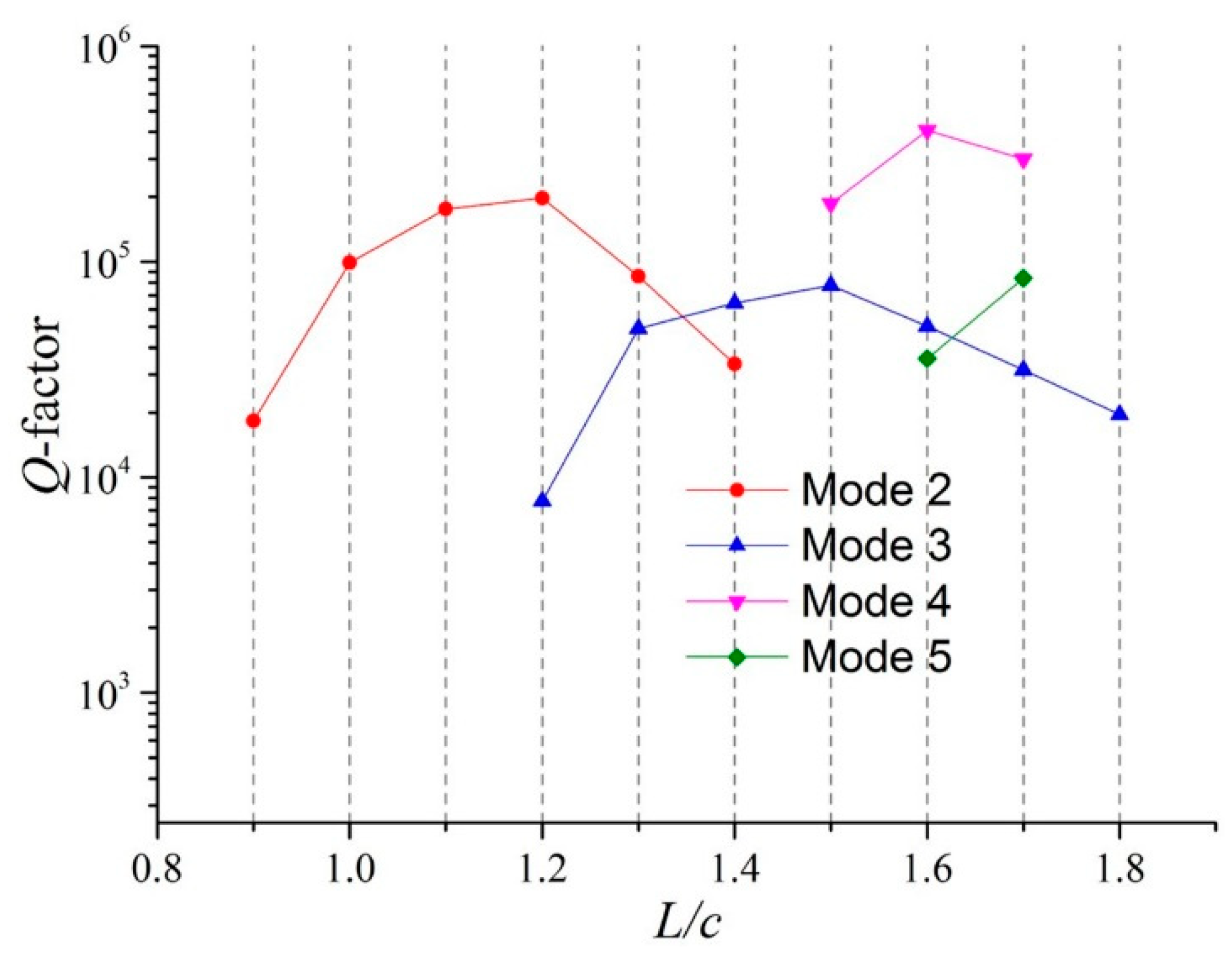
4. Numerical Results

In this section, we use the finite-difference time-domain (FDTD) method to simulate the cavity mode estimating the resonant mode frequency and Q-factor in various defects when changing the size of the defect L from 0.1c–2c. A broadband dipole source whose bandwidth covers the complete photonic bandgap is positioned at the center of the cavity and along the z-axis. We demonstrate that effective mode volumes of the cavity mode could be suppressed by making the defect smaller, and Q-factors of cavities can become high when the resonant frequency is located around the center of the complete photonic bandgap. Figure 4 illustrates all the high Q-factor cavity modes we find near and inside the photonic bandgap as the defect size L is increased. The dashed lines indicate the boundary of the complete photonic bandgap and the position of the bandgap center related to the woodpile template without a defect. We find that high Q-factor cavity modes do not exist far outside the bandgap as expected although some of them appear at the band edge. Furthermore, the normalized resonant frequency of both fundamental modes (Mode 1) and high order modes (Mode 2–5) decreases when increasing the defect size L. The calculated Q-factors for the fundamental modes (Mode 1, black square in Figure 4) are shown in Figure 5 as a function of normalized resonant frequency when defect size L ranges from 0.1c–0.8c. The Q-factor reaches its maximum value near the middle of the photonic bandgap when defect size L = 0.25c. As we use a finite structure in our simulation, the reflectivity drops when the frequency moves away from the bandgap center resulting in a drop of the Q-factor.
For those cavity modes inside the complete photonic bandgap when the defect size 0.15cL ≤ 0.6c, the calculated normalized mode volumes are shown along with the Q-factors in Figure 6. It is shown that the calculated normalized mode volume reduces from 0.64 to 0.29 (λ/n)3 when the defect size L decreases from 0.4c to 0.15c, while Q-factor reaches the highest value of 1.24 × 10⁵ when L = 0.25c and starts to drop quickly if the defect size is further reduced. As the cavity mode approaches the band edge the mode volume reaches a minimum because the field outside the bandgap is not confined. For L > 0.4c the mode volume appears to decrease slightly which may be a consequence of limited calculation space when the mode approaches the band edge and becomes leaky. Figure 7 illustrates the energy distribution of cavity modes when defect size L = 0.5c, L = 0.25c, L = 0.2c and L = 0.15c, respectively. In Figure 7, we observe nearly perfect Gaussian confinement in such defects with “wings” (predominantly blue areas) floating inside the adjacent dielectric rods. Furthermore, we see that better confinement of the energy distribution of the cavity modes can be achieved by reducing the defect size L from 0.5c to 0.15c when the intensity of the “wings” becomes weaker and weaker.
In Figure 4 we noticed that multiple modes can coexist in the cavity when defect size increase. To show the difference between these modes, we plot their energy distributions in Figure 8. The 2D snapshots are taken through the center of the cavity in xy-plane. As cavity modes with the same order share a similar mode pattern, we label them from Mode 1 to Mode 5 to distinguish them.
Figure 9 shows the calculated Q-factors for high order cavity modes when defect size 0.9cL ≤ 1.8c. Like the Q-factor of fundamental modes (Mode 1) plotted in Figure 5, the Q-factor of cavity modes within the same order also increases first and then decreases when the mode frequency drops from the upper edge to the lower edge of the photonic bandgap, which means that modes appear to be leaky when they approach the band edge due to the lack of the confinement from the structure. Limited numbers of results were obtained for Mode 4 and 5 but are included here for completeness.

5. Discussion and Conclusions

In all cases in this paper, the dipole is oscillating along the z-axis. In a more general situation, a dipole could be in any orientation and other Ex or Ey modes (in which case the Ex or Ey component could be much greater than Ez component) could be excited. The reason only z-axis orientated case is discussed here is, as we decrease the defect size in xy-plane, we found that the Ex and Ey modes are dramatically suppressed and only Ez modes survive in such a cavity (see Figure S1 in the supplementary materials). It means the confined cavity mode is polarized along the z-axis when the defect size L is small enough. In general, the resulting resonant mode in a cavity surrounded by PhC structure with complete photonic bandgap could be considered a combination between cavity mode itself without PhC structure and the confinement of complete photonic bandgap. However, the mode distribution in a 3D PhC structure is strongly affected by the surrounding environment. It leads to a great complexity of the investigation due to kinds of potential defect positions. In this paper we demonstrate that, by carefully choosing the position of the defect at the lattice center, a cavity with high symmetry can support well confined Gaussian-like cavity modes and the analysis of such cavities can be greatly simplified by using symmetrical lattices. We find that high Q-factor cavities can be obtained when the resonant frequency close to the center of the photonic bandgap and small mode volumes of the resonant modes can be achieved by reducing the cavity size. Furthermore, we can tune the size of the cavity and manually choose the cavity mode with desired frequency. Additionally, the patterns of the resonant modes investigated in this paper can then be used for the examination of mode orders. In the future, we could introduce light emitters in such cavities to control the spontaneous-emission and design waveguides to couple cavity modes out. As an example, we provide our preliminary work on the fabrication of polymer woodpile structures with incorporated defects using DLW method in the supplementary materials (Figure S2). In the long term, the investigation of manipulating the light propagation and confinement in woodpile could lead to the ultimate template for photonic integrated circuits and optical computers.

Supplementary Materials

The following are available online at https://www.mdpi.com/2076-3417/8/7/1087/s1, Figure S1: Amplitude of the electric field (Ex, Ey and Ez component) of Ex mode (a–c) and Ez mode (d–f) as a function of time and their corresponding fast Fourier transform when defect size L = 0.25c, Figure S2: Scanning electron microscopy images of the fabricated polymer woodpile structures using the DLW method, (a) with various defects introduced (b) with dye doped defects embedded.

Author Contributions

Conceptualization, X.Z. and Y.-L.D.H.; Data curation, X.Z. and M.P.C.T.; Formal analysis, X.Z.; Funding acquisition, Y.-L.D.H. and J.G.R.; Investigation, X.Z. and M.P.C.T.; Project administration, Y.-L.D.H. and J.G.R.; Software, X.Z. and M.P.C.T.; Supervision, Y.-L.D.H. and J.G.R.; Visualization, X.Z.; Writing (original draft), X. Z; Writing (review & editing), X.Z., Y.-L.D.H. and J.G.R.

Funding

This research was funded by the Engineering and Physical Sciences Research Council (EPSRC) grant number EP/M009033/1 and EP/M024458/1.

Acknowledgments

This work was carried out using the computational facilities of the Advanced Computing Research Centre, University of Bristol, Bristol, UK and funded by the Engineering and Physical Sciences Research Council (EPSRC) grant EP/M009033/1 and EP/M024458/1.

Conflicts of Interest

The authors declare no conflict of interest. The funders had no role in the design of the study; in the collection, analyses, or interpretation of data; in the writing of the manuscript, and in the decision to publish the results.

References

  1. Joannopoulos, J.D.; Johnson, S.G.; Winn, J.N.; Meade, R.D. Photonic Crystals: Molding the Flow of Light, 2nd ed.; Princeton University Press: Princeton, NJ, USA, 2008. [Google Scholar]
  2. Yablonovitch, E. Inhibited Spontaneous Emission in Solid-State Physics and Electronics. Phys. Rev. Lett. 1987, 58, 2059–2062. [Google Scholar] [CrossRef] [PubMed]
  3. John, S. Strong localization of photons in certain disordered dielectric superlattices. Phys. Rev. Lett. 1987, 58, 2486–2489. [Google Scholar] [CrossRef] [PubMed]
  4. Yablonovitch, E.; Gmitter, T.J. Photonic band structure: The face-centered-cubic case. Phys. Rev. Lett. 1989, 63, 1950–1953. [Google Scholar] [CrossRef] [PubMed]
  5. Datta, S.; Chan, C.T.; Ho, K.M.; Soukoulis, C.M. Photonic Band Gaps in Experimentally Realizable Periodic Dielectric Structures. Europhys. Lett. 1991, 16, 563–568. [Google Scholar]
  6. Datta, S.; Chan, C.T.; Ho, K.M.; Soukoulis, C.M. Photonic bandgaps in periodic dielectric structures: The scalar-wave approximation. Phys. Rev. B 1992, 46, 10650. [Google Scholar] [CrossRef]
  7. Chan, C.T.; Datta, S.; Ho, K.M.; Soukoulis, C.M. A7 structure: A family of photonic crystals. Phys. Rev. B 1994, 50, 1988–1991. [Google Scholar] [CrossRef]
  8. Maldovan, M.; Thomas, E.L. Diamond-structured photonic crystals. Nat. Mater. 2004, 3, 593–600. [Google Scholar] [CrossRef] [PubMed]
  9. Yablonovitch, E.; Gmitter, T.J.; Leung, K.M. Photonic band structure: The face-centered-cubic case employing nonspherical atoms. Phys. Rev. Lett. 1991, 67, 2295–2298. [Google Scholar] [CrossRef] [PubMed]
  10. Ho, K.M.; Chan, C.T.; Soukoulis, C.M.; Biswas, R.; Sigalas, M. Photonic band gaps in three dimensions: New layer-by-layer periodic structures. Solid State Commun. 1994, 89, 413–416. [Google Scholar] [CrossRef]
  11. Chutinan, A.; John, S. Light localization for broadband integrated optics in three dimensions. Phys. Rev. B 2005, 72, 161316(R). [Google Scholar] [CrossRef]
  12. Chutinan, A.; John, S. 3+1 dimensional integrated optics with localized light in a photonic band gap. Opt. Express 2006, 14, 1266. [Google Scholar] [CrossRef] [PubMed]
  13. Ishizaki, K.; Koumura, M.; Suzuki, K.; Gondaira, K.; Noda, S. Realization of three-dimensional guiding of photons in photonic crystals. Nat. Photonics 2013, 7, 133–137. [Google Scholar] [CrossRef]
  14. Gondaira, K.; Ishizaki, K.; Kitano, K.; Asano, T.; Noda, S. Control of radiation angle by introducing symmetric end structure to oblique waveguide in three-dimensional photonic crystal. Opt. Express 2016, 24, 13518. [Google Scholar] [CrossRef] [PubMed]
  15. Braun, P.V.; Rinne, S.A.; García-Santamaría, F. Introducing defects in 3D photonic crystals: State of the art. Adv. Mater. 2006, 18, 2665–2678. [Google Scholar] [CrossRef]
  16. Okano, M.; Chutinan, A.; Noda, S. Analysis and design of single-defect cavities in a three-dimensional photonic crystal. Phys. Rev. B 2002, 66, 165211. [Google Scholar] [CrossRef]
  17. Ho, Y.-L.D.; Ivanov, P.S.; Engin, E.; Nicol, M.F.J.; Taverne, M.P.C.; Cryan, M.J.; Craddock, I.J.; Railton, C.J.; Rarity, J.G. FDTD Simulation of Inverse Three-Dimensional Face-centered Cubic Photonic Crystal Cavities. IEEE J. Quantum Electron 2011, 47, 1480–1492. [Google Scholar] [CrossRef]
  18. Imagawa, S.; Edagawa, K.; Notomi, M. Strong light confinement in a photonic amorphous diamond structure. Appl. Phys. Lett. 2012, 100, 151103. [Google Scholar] [CrossRef] [Green Version]
  19. Tajiri, T.; Takahashi, S.; Tandaechanurat, A.; Iwamoto, S.; Arakawa, Y. Design of a three-dimensional photonic crystal nanocavity in a <110>-layered diamond structure. Jpn. J. Appl. Phys. 2014, 53, 04EG08. [Google Scholar] [CrossRef]
  20. Taverne, M.P.C.; Ho, Y.-L.D.; Rarity, J.G. Investigation of defect cavities formed in three-dimensional woodpile photonic crystals. J. Opt. Soc. Am. B 2015, 32, 639. [Google Scholar] [CrossRef] [Green Version]
  21. Taverne, M.P.C.; Ho, Y.-L.D.; Zheng, X.; Liu, S.; Chen, L.-F.; Lopez-Garcia, M.; Rarity, J.G. Investigation of Defect Cavities Formed in Inverse Three-Dimensional Rod-Connected Diamond Photonic Crystals. Europhys. Lett. 2016, 116, 64007. [Google Scholar] [CrossRef]
  22. Woldering, L.A.; Mosk, A.P.; Vos, W.L. Design of a three-dimensional photonic band gap cavity in a diamondlike inverse woodpile photonic crystal. Phys. Rev. B 2014, 90. [Google Scholar] [CrossRef]
  23. Nomura, M.; Iwamoto, S.; Kumagai, N.; Arakawa, Y. Ultralow threshold photonic crystal nanocavity laser. Phys. E 2008, 40, 1800–1803. [Google Scholar] [CrossRef]
  24. Matsuo, S.; Shinya, A.; Kakitsuka, T.; Nozaki, K.; Segawa, T.; Sato, T.; Kawaguchi, Y.; Notomi, M. High-speed ultracompact buried heterostructure photonic-crystal laser with 13 fJ of energy consumed per bit transmitted. Nat. Photonics 2010, 4, 648–654. [Google Scholar] [CrossRef]
  25. Cao, D.; Tandaechanurat, A.; Nakayama, S.; Ishida, S.; Iwamoto, S.; Arakawa, Y. Silicon-based three-dimensional photonic crystal nanocavity laser with InAs quantum-dot gain. Appl. Phys. Lett. 2012, 101, 191107. [Google Scholar] [CrossRef]
  26. Lončar, M.; Yoshie, T.; Scherer, A.; Gogna, P.; Qiu, Y. Low threshold photonic crystal laser. Appl. Phys. Lett. 2002, 81, 2680–2682. [Google Scholar] [CrossRef]
  27. Loncar, M.; Scherer, A.; Qiu, Y.M. Photonic crystal laser sources for chemical detection. Appl. Phys. Lett. 2003, 82, 4648–4650. [Google Scholar] [CrossRef]
  28. Chow, E.; Grot, A.; Mirkarimi, L.W.; Sigalas, M.; Girolami, G. Ultracompact biochemical sensor built with two-dimensional photonic crystal microcavity. Opt. Lett. 2004, 29, 1093. [Google Scholar] [CrossRef] [PubMed]
  29. Lee, M.R.; Fauchet, P.M. Nanoscale microcavity sensor for single particle detection. Opt. Lett. 2007, 32, 3284. [Google Scholar] [CrossRef] [PubMed]
  30. Baba, T. Photonic Crystal Nanolaser Biosensors. MRS Commun. 2015, 5, 1. [Google Scholar] [CrossRef]
  31. Johnson, P.M.; Koenderink, A.F.; Vos, W.L. Ultrafast switching of photonic density of states in photonic crystals. Phys. Rev. B 2002, 66, 081102. [Google Scholar] [CrossRef]
  32. Nozaki, K.; Tanabe, T.; Shinya, A.; Matsuo, S.; Sato, T.; Taniyama, H.; Notomi, M. Sub-femtojoule all-optical switching using a photonic crystal nanocavity. Nat. Photonics 2010, 4, 477–483. [Google Scholar] [CrossRef]
  33. Volz, T.; Reinhard, A.; Winger, M.; Badolato, A.; Hennessy, K.J.; Hu, E.L.; Imamoğlu, A. Ultrafast all-optical switching by single photons. Nat. Photonics 2012, 6, 605–611. [Google Scholar] [CrossRef]
  34. Chen, W.; Beck, K.M.; Bücker, R.; Gullans, M.; Lukin, M.D.; Tanji-Suzuki, H.; Vuletic, V. All-optical switch and transistor gated by one stored photon. Science 2013, 341, 768–770. [Google Scholar] [CrossRef] [PubMed]
  35. Fushman, I.; Englund, D.; Faraon, A.; Stoltz, N.; Petroff, P.; Vučković, J. Controlled phase shifts with a single quantum dot. Science 2008, 320, 769–772. [Google Scholar] [CrossRef] [PubMed]
  36. Xiao, Y.-F.; Gao, J.; Zou, X.-B.; McMillan, J.F.; Yang, X.; Chen, Y.-L.; Han, Z.-F.; Guo, G.-C.; Wong, C.W. Coupled quantum electrodynamics in photonic crystal cavities towards controlled phase gate operations. New J. Phys. 2008, 10, 123013. [Google Scholar] [CrossRef] [Green Version]
  37. Young, A.; Hu, C.Y.; Marseglia, L.; Harrison, J.P.; O’Brien, J.L.; Rarity, J.G. Cavity enhanced spin measurement of the ground state spin of an NV center in diamond. New J. Phys. 2009, 11, 013007. [Google Scholar] [CrossRef] [Green Version]
  38. Lodahl, P.; Mahmoodian, S.; Stobbe, S. Interfacing single photons and single quantum dots with photonic nanostructures. Rev. Mod. Phys. 2015, 87, 347–400. [Google Scholar] [CrossRef] [Green Version]
  39. Sánchez, A.; Porta, A.V.; Orozco, S. Photonic band-gap and defect modes of a one-dimensional photonic crystal under localized compression. J. Appl. Phys. 2017, 121. [Google Scholar] [CrossRef]
  40. Chen, C.-P.; Tetsuo, A.; Stephen, G.; Trevor, M.B.; Phillip, S. A Novel Photonic Crystal Band-pass Filter Using Degenerate Modes of A Point-defect Microcavity for Terahertz Communication Systems. Microw. Opt. Technol. Lett. 2014, 56, 792–797. [Google Scholar] [CrossRef]
  41. Chen, C.; Li, X.; Li, H.; Xu, K.; Wu, J.; Lin, J. Bandpass filters based on phase-shifted photonic crystal waveguide gratings. Opt. Soc. Am. 2007, 15, 237–241. [Google Scholar] [CrossRef]
  42. Costa, R.; Melloni, A.; Martinelli, M. Bandpass resonant filters in photonic-crystal waveguides. IEEE Photonics Technol. Lett. 2003, 15, 401–403. [Google Scholar] [CrossRef]
  43. Maruo, S.; Nakamura, O.; Kawata, S. Three-dimensional microfabrication with two-photon-absorbed photopolymerization. Opt. Lett. 1997, 22, 132. [Google Scholar] [CrossRef] [PubMed]
  44. Hermatschweiler, M.; Ledermann, A.; Ozin, G.A.; Wegener, M.; von Freymann, G. Fabrication of Silicon Inverse Woodpile Photonic Crystals. Adv. Funct. Mater. 2007, 17, 2273–2277. [Google Scholar] [CrossRef] [Green Version]
  45. T´etreault, N.; von Freymann, G.; Deubel, M.; Hermatschweiler, M.; P´erez-Willard, F.; John, S.; Wegener, M.; Ozin, G.A. New route to three-dimensional photonic bandgap materials: Silicon double inversion of polymer templates. Adv. Mater. 2006, 18, 457–460. [Google Scholar]
  46. Staude, I.; Thiel, M.; Essig, S.; Wolff, C.; Busch, K.; von Freymann, G.; Wegener, M. Fabrication and characterization of silicon woodpile photonic crystals with a complete bandgap at telecom wavelengths. Opt. Lett. 2010, 35, 1094. [Google Scholar] [CrossRef] [PubMed]
  47. Staude, I.; von Freymann, G.; Essig, S.; Busch, K.; Wegener, M. Waveguides in three-dimensional photonicbandgap materials by direct laser writing and silicon double inversion. Opt. Lett. 2011, 36, 67. [Google Scholar] [CrossRef] [PubMed]
  48. Chen, L.-F.; Taverne, M.P.C.; Zheng, X.; Oulton, R.; Lin, J.-D.; Lopez-Garcia, M.; Ho, Y.-L.D.; Rarity, J.G. Evidence of Near-Infrared Partial Photonic Bandgap in Polymeric Rod-connected Diamond Structure. Opt. Express 2015, 23, 26565. [Google Scholar] [CrossRef] [PubMed]
  49. Ishizaki, K.; Noda, S. Manipulation of photons at the surface of three-dimensional photonic crystals. Nature 2009, 460, 367–370. [Google Scholar] [CrossRef] [PubMed]
  50. Ogawa, S.; Imada, M.; Yoshimoto, S.; Okano, M.; Noda, S. Control of light emission by 3D photonic crystals. Science 2004, 305, 227–229. [Google Scholar] [CrossRef] [PubMed]
  51. Yang, Y.; Huang, Y. Mode characteristics and directional emission for square microcavity lasers. J. Phys. D Appl. Phys. 2016, 49, 253001. [Google Scholar] [CrossRef]
  52. Johnson, S.G.; Joannopoulos, J. Block-iterative frequency domain methods for Maxwell’s equations in a planewave basis. Opt. Express 2001, 8, 173. [Google Scholar] [CrossRef] [PubMed]
  53. Railton, C.; Hilton, G. The analysis of medium-sized arrays of complex elements using a combination of FDTD and reaction matching. IEEE Trans. Antennas Propag. 1999, 47, 707. [Google Scholar] [CrossRef] [Green Version]
  54. Mandelshtam, V.A.; Taylor, H.S. Harmonic inversion of time signals and its applications. J. Chem. Phys. 1997, 107, 6756–6769. [Google Scholar] [CrossRef]
Figure 1. (a) Parameters of the woodpile structure defined in the simulation: vertical period c, height of rods h = c/4, distance between adjacent logs d = c/√2 and width of rods w. The refractive index of rods is nrod = 3.3, while the background material is air nair = 1; (b) The calculated band structure by using plane-wave expansion (PWE) method [52] with optimized parameters. The complete photonic bandgap reaches a maximum value of 15.88% when w = 0.21c [20]. The insets illustrate the symmetric points in Brillouin zone of the face-centered-cubic (FCC) lattice relative to the woodpile and the calculation routes to obtain the complete photonic bandgap.
Applsci 08 01087 g001
Figure 2. The location of the defect in one vertical period (four stacking layers in the z direction). (a) view of the xz-plane (b) view of the yz-plane (c) view of the xy-plane (from the top) and (d) the free 3D view. L is the size of the defect in x and y direction while the height is always 2h to make it connect with both rods at the bottom and top.
Applsci 08 01087 g002
Figure 3. The comparison between rod-connected diamond lattice (a) and woodpile lattice (b). Woodpile could be considered as a layered version of the rod-connected diamond structure [8].
Applsci 08 01087 g003
Figure 4. Normalized resonant frequency (c/λ) as a function of defect size L. The dashed lines indicate the boundary of the complete photonic bandgap and the position of the bandgap center related to the woodpile template without a defect.
Applsci 08 01087 g004
Figure 5. Calculated Q factors for fundamental cavity modes (Mode 1) as a function of normalized resonant frequency when defect size L varies from 0.1c to 0.8c.
Applsci 08 01087 g005
Figure 6. Calculated Q factor and normalized mode volume of Mode 1 as a function of defect size L from 0.15c to 0.6c.
Applsci 08 01087 g006
Figure 7. Energy distribution of cavity modes when defect size (a) L = 0.5c; (b) L = 0.25c; (c) L = 0.2c and (d) L = 0.15c.
Applsci 08 01087 g007
Figure 8. The energy distribution of the high order modes in xy-plane: (a) the mode pattern of Mode 1 when normalized frequency c/λ = 0.481 and L = 0.8c; (b) the mode pattern of Mode 2 when normalized frequency c/λ = 0.506 and L = 1.2c; (c) the mode pattern of Mode 3 when normalized frequency c/λ = 0.568 and L = 1.2c; (d) the mode pattern of Mode 4 when normalized frequency c/λ = 0.522 and L = 1.7c; (e) the mode pattern of Mode 5 when normalized frequency c/λ = 0.534 and L = 1.7c.
Applsci 08 01087 g008
Figure 9. The calculated Q-factor for the various higher order cavity modes as a function of defect size L.
Applsci 08 01087 g009

