Article

An AC/DC LED Driver with Unity Power Factor and Soft Switching

1
Department of Electrical Engineering, National Formosa University, Yunlin County 63201, Taiwan
2
Department of Electrical Engineering, I-Shou University, Kaohsiung 84001, Taiwan
3
Department Electrical Engineering, Far East University, Tainan 74448, Taiwan
*
Author to whom correspondence should be addressed.
Appl. Sci. 2018, 8(5), 780; https://doi.org/10.3390/app8050780
Submission received: 8 April 2018 / Revised: 10 May 2018 / Accepted: 10 May 2018 / Published: 14 May 2018

Abstract

:
Traditional light-emitting diode (LED) drivers with pulse-width modulation (PWM)-type converters suffer the problem of hard switching, leading to low circuit efficiency and low reliability. LED drivers supplied by alternating current (AC) line source generally require using an additional power-factor correction (PFC) stage to satisfy the regulations on power factor (PF) and total current harmonic distortion (THDi). It results in more circuit losses, especially when the active switch of the PFC stage operates at hard switching. This paper presents an alternating current-to-direct current (AC/DC) converter for driving high-brightness LEDs with the features of soft switching and high PF. The proposed single-stage circuit is formed by integrating a buck–boost converter and a buck converter. By elaborately rearranging the wirings between the circuit components of both converters, the power MOSFETs can be switched on at zero voltage. The operating modes at steady-state are analyzed and the mathematical equations for deriving circuit parameters are conducted. Finally, a prototype circuit for driving 60-W LEDs was built and measured. Based on the experimental results, the feasibility and satisfactory performance of the proposed LED driver are proved.

1. Introduction

Nowadays, high-brightness light-emitting diodes (LEDs) are popularly used to replace incandescent and fluorescent lamps in many applications owing to their advantages of small size, high luminous efficiency, long lifespan, high reliability, and environmental friendliness [1,2,3]. On the purpose of increasing the utilization factor of the power electric equipment and reduce the electromagnetic interference (EMI), some regulations such as IEC 61000-3-2 and IEEE 519, are enacted to restrict the power factor (PF) and total current harmonic distortion (THDi) of the alternating current-to-direct current (AC/DC) LED drivers to a reasonable range. In order to meet these regulations, an additional converter serving as a power-factor correction (PFC) stage is added to a DC/DC converter of which the output voltage is adjusted to drive LEDs. It results in a LED driver with two power-process stages. Although the two-stage approaches have satisfactory performance, they are not cost-effective products since two converters and two corresponding control circuits are required. In addition, the two-stage approaches take two energy-conversion processes, and hence produce more losses including switching loss and conduction loss. Aiming to solve the shortcomings of the two-stage approaches, many single-stage LED drivers have been proposed by integrating the PFC stage and the DC/DC stage [4,5,6,7,8,9,10].
Among the single-stage approaches, one power switch is commonly shared by the PFC stage and the DC/DC stage. Hence, they only use one control circuit and own the benefits of less component count and simply circuit topology. Nevertheless, the shared power switch should handle the current in both power-conversion stages, leading to more conducting losses. Moreover, the power switches of the single-stage approaches usually operate at hard switching and suffer the problem of high switching losses and high voltage and current stresses.
To further improve the circuit efficiency, literature proposed single-stage converters of which the power switches can fulfill soft switching to effectively reduce the switching losses [11,12,13]. Also, high PF and low THDi can be achieved. Unfortunately, there are still some defects required to be improved. In Reference [11], a coupled inductor is used in the buck–boost converter and its leakage inductance would incur high spike voltage across the power switch. In Reference [12], a boost converter serves as the PFC converter. Figure 1 shows the circuit topology that was proposed in Reference [12]. It integrates a boost converter and a buck converter. The boost converter serves as a PFC stage while the buck converter outputs a stable voltage to drive the load. High PF can be achieved, provided that the boost converter is operated at discontinuous current mode (DCM). However, a boost-typed PFC converter needs a high DC-link voltage to ensure DCM operation. It causes the circuit to require the use of high voltage rated components. For pursuing a better solution, this paper proposes a novel AC/DC converter to drive high power LEDs. The proposed circuit mainly consists of a buck–boost converter and a buck converter. Different from the circuit of Reference [12], when the boost-buck converter operates at DCM, it can obtain high power factor without needing a high DC-link voltage. A prototype circuit of 60-W was built and tested to verify the analytical predictions. Satisfactory performance is obtained from the experimental results.

2. Proposed Circuit Topology and Operation Analysis

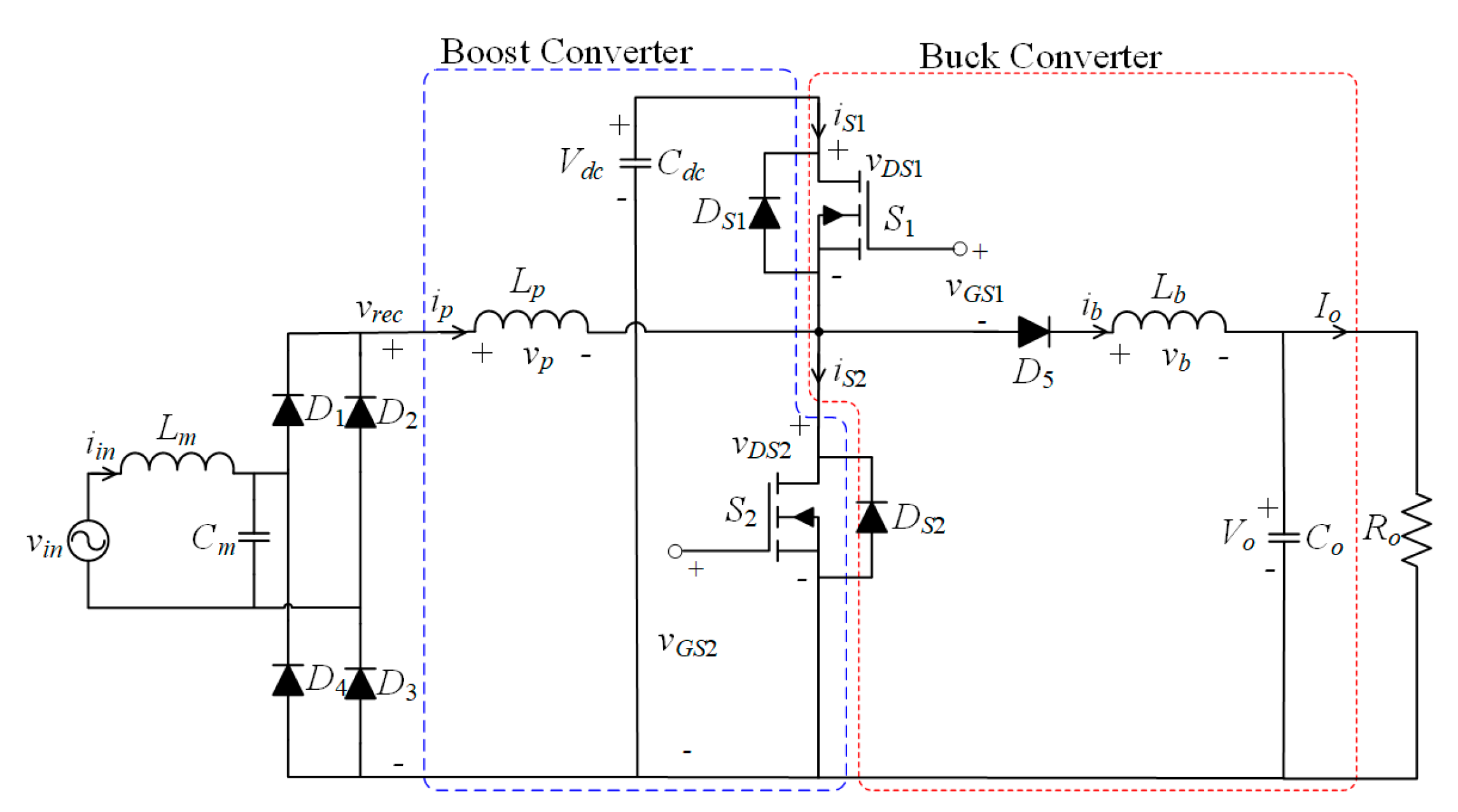
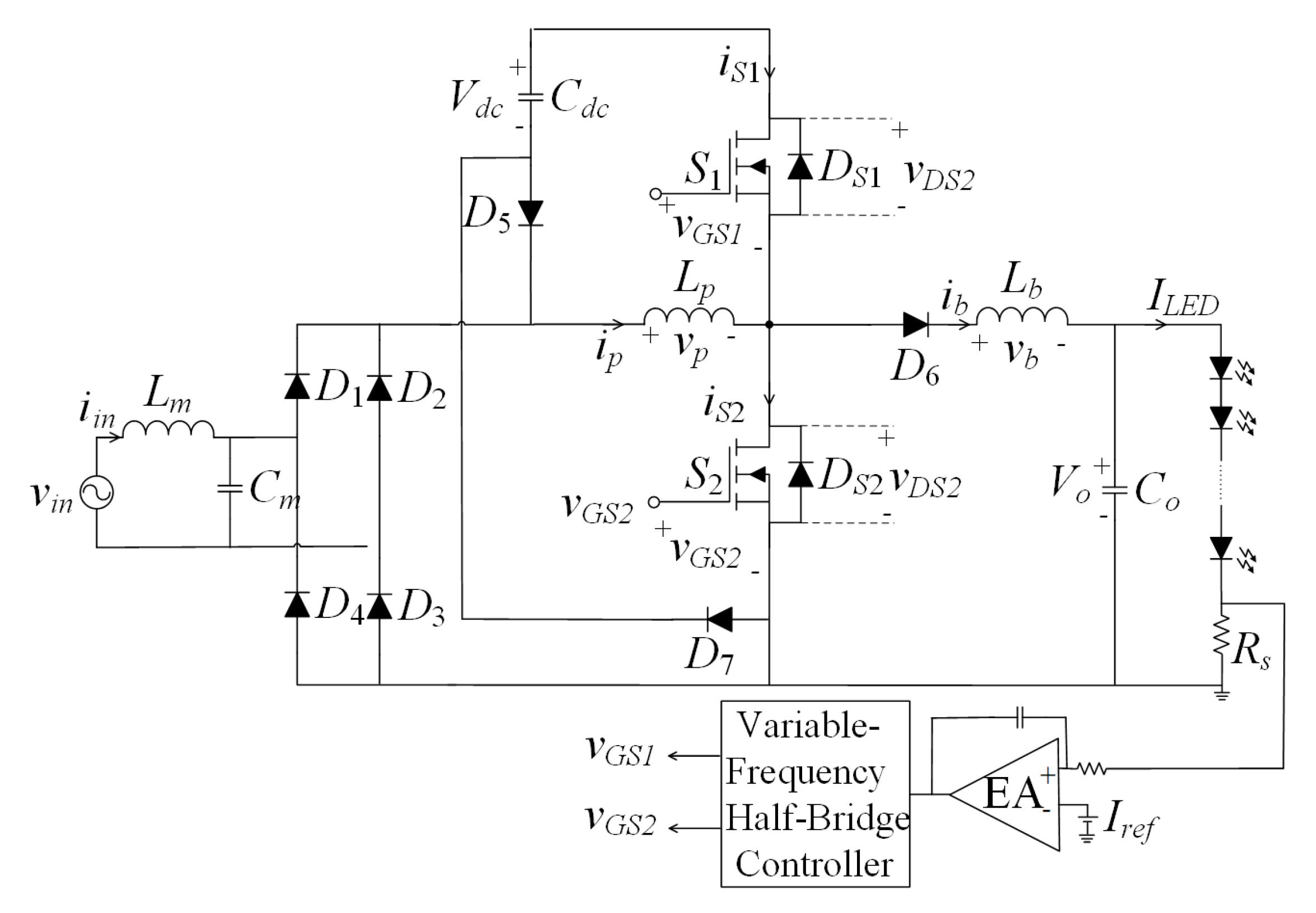
2.1. Circuit Topology

The proposed AC/DC LED driver is derived by integrating a buck–boost converter and a buck converter, as shown in Figure 2. Two MOSFETs serve as the active switches, S1 and S2. The diodes DS1 and DS2 are the intrinsic diodes of S1 and S2, respectively. The buck–boost converter is formed by Lp, S2, DS1, D5, and Cdc. The buck converter is formed by Lb, S1, DS2, D6, D7, and Co. The low-pass filter is composed of Lm and Cm. The control circuit is mainly a half-bridge controller that is widely adopted to control the active switches of a Class-D inverter. The power switches S1 and S2 are driven by two gated voltage, vGS1 and vGS2. They are nonoverlapping and complementary rectangular-wave waveform. There is a short duration called deadtime. During the deadtime, both vGS1 and vGS2 are zero volts. Neglecting the deadtime, both vGS1 and vGS2 have a duty ratio of 0.5.
As compared to the circuit topology proposed in Reference [12], the proposed one uses a buck–boost converter to serve the PFC stage while that of Reference [12] uses a boost converter. It is known that both converters operating at DCM can achieve nearly unity power factor. Nevertheless, when using a boost-typed PFC converter, it requires very high DC-link voltage to ensure unity power factor [14]. Although the proposed circuit needs to use two additional diodes, the voltage ratings of the circuit components could be lower than that of Reference [12].

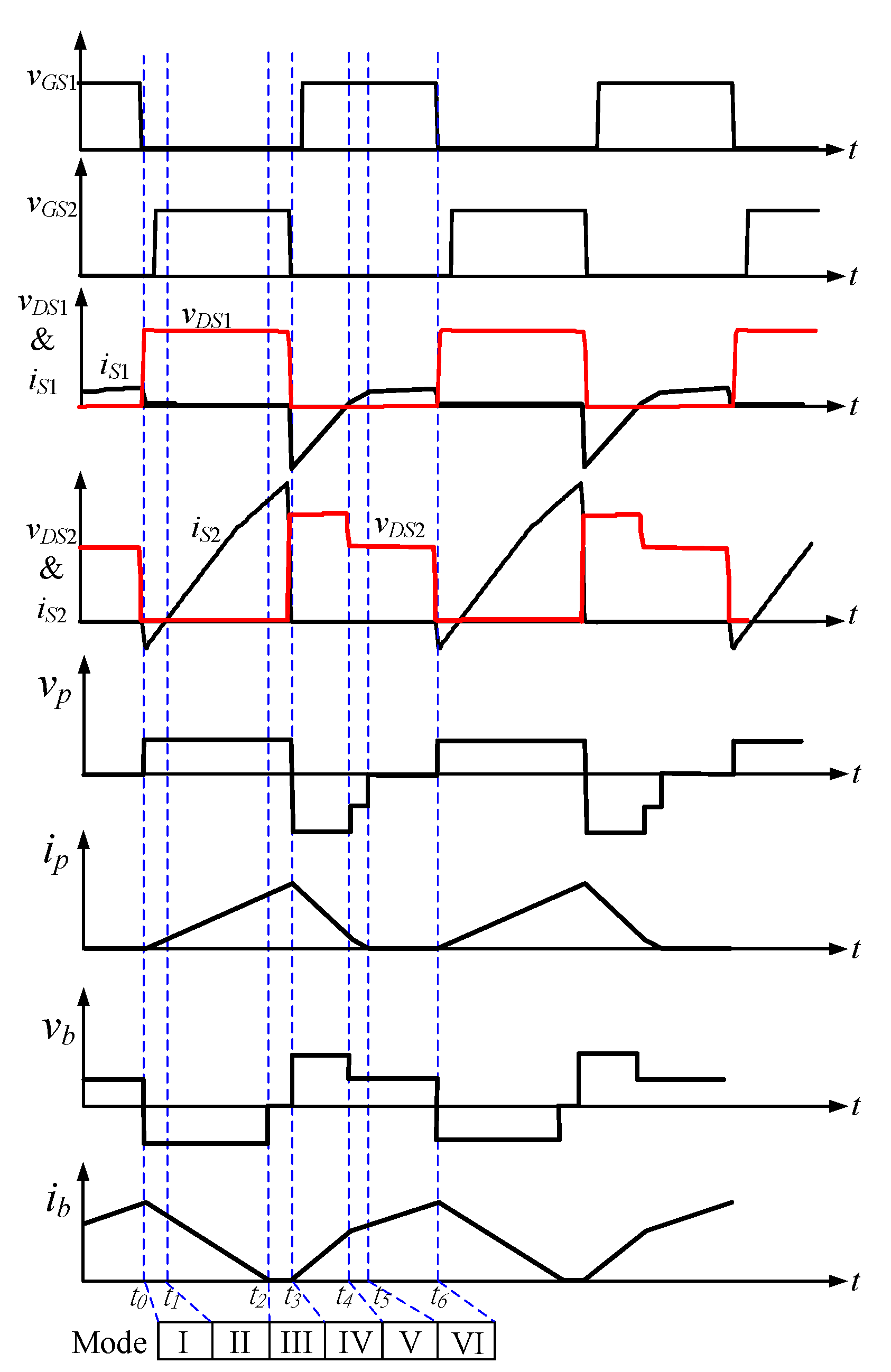
2.2. Operation Analysis

For simplifying the circuit analysis, the following assumptions are made:
  • All the semiconductor devices are ideal except that the parasitic capacitances and the intrinsic diodes of the MOSFETs are considered.
  • The DC-link capacitor Cdc and the output capacitor Co are both large enough; thus, the DC-link voltage Vdc and the output voltage Vo can be regarded as constant.
  • The switching frequency of the active switches, fs, is much higher than that of the input-line voltage, fs. Hence, the input-line voltage is considered as constant during each high-frequency cycle.
At steady-state operation, the circuit operation can be divided into six modes in one high-frequency cycle. In order to make both power switches achieve zero-voltage switching (ZVS), both converters should be operated at DCM. These six operation modes are shown in Figure 3, where vrec represents the rectified input voltage. The illustrative current and voltage waveforms of some key components are shown in Figure 4.

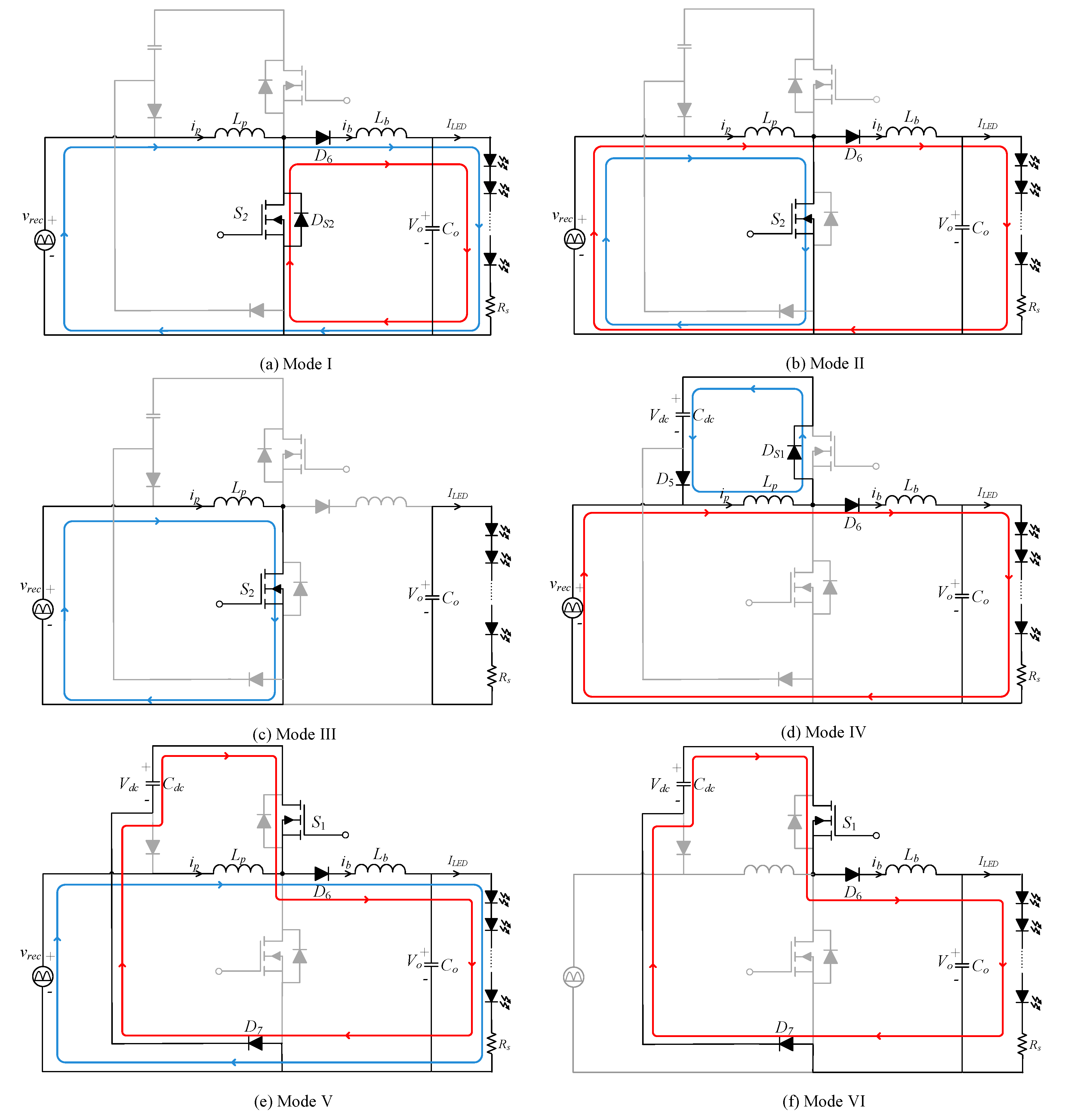
2.2.1. Mode I (t0 < t < t1; in Figure 3a)

Prior to this mode, S1 is on and the DC link voltage Vdc supplies the buck-inductor current ib. Mode I begins at the instant of turning off S1. Thereby, ib would discharge the parasitic capacitance (CDS2) between the drain and source of S2. As soon as the voltage across CDS2 decreases to −0.7 V, DS2 is forward-biased to conduct ib. The gated voltage vGS2 becomes high level after the short deadtime and the current flowing through DS2 diverts to flow from the source to drain of the MOSFET S2. By this way, the voltage across S2 is clamped at near zero voltage. The voltage across the buck inductor Lb is minus of the output voltage Vo and hence, ib decreases linearly.
v b ( t ) = V o
i b ( t ) = i b ( t 0 ) V o L b ( t t 0 )
Since S2 is on, the voltage across the buck–boost inductor Lp is equal to vrec.
v p ( t ) = v r e c ( t ) = V m | s i n ( 2 π f L t ) | ,
where fL and Vm respectively represent the frequency and the amplitude of the input-line voltage.
Since the buck–boost converter is operated at DCM, the buck–boost current ip linearly increases from zero.
i p ( t ) = v r e c ( t ) L p ( t t 0 ) = V m | s i n ( 2 π f L t ) | L p ( t t 0 )
In this mode, ib is higher than ip. There are two current loops for ib. Parts of ib flow through S2, while the rest of ib is equal to ip, which flows through Lp and the line-voltage source. This mode ends when ip becomes higher than ib.

2.2.2. Mode II (t1 < t < t2; in Figure 3b)

At the beginning of Mode II, ip becomes higher than ib and the current flowing through S2 changes direction. Parts of ip flow through S2 from its drain to source, while the rest flows to the buck converter. The voltage and current equations for vb, vp, ib and ip are the same as (1)–(4) in Mode I. The current ib keeps decreasing and ip keeps increasing. When ib decreases to zero, Mode II ends.

2.2.3. Mode III (t2 < t < t3; in Figure 3c)

The current ib is zero. S2 is kept on and ip continues to increase. Mode III ends when the gated voltage vGS2 becomes low level to turn off S2, and the circuit operation enters Mode IV.

2.2.4. Mode IV (t3 < t < t4; in Figure 3d)

The current ip reach a peak value of each high-frequency cycle at the instant of turning off S2. The current ip will be diverted from S2 to discharge the parasitic capacitance (CDS1) between the drain and source of S1. As soon as the voltage across CDS1 decreases to −0.7 V, DS1 is forward biased to conduct ip. The gated voltage vGS1 becomes high level after the short deadtime and ip diverts from DS1 to flow through S1 from its source to drain. By this way, the voltage across S1 is clamped at near zero voltage. Now, the current loop of ip is LpS1CdcD5 and the DC-link capacitance Cdc is charged. The voltage across Lp is equal to −Vdc and hence, ip decrease linearly.
v p ( t ) = V d c
i p ( t ) = i p ( t 3 ) V d c L p ( t t 3 )
On the other hand, the current ib starts to increase from zero with the current loop: LpD6LbCovrec. The voltage and current equations for the buck inductor can be expressed as:
v b = v r e c ( t ) + V d c V o ,
i b ( t ) = V m | s i n ( 2 π f L t ) | + V d c V o L b ( t t 3 ) .
In this mode, ip is higher than ib. There are two current loops for ip. Parts of ip flow through S1 to charge Cdc, while its residual is equal to ib and flows into the buck converter. This mode ends when ib becomes higher than ip.

2.2.5. Mode V (t4 < t < t5; in Figure 3e)

At the beginning of Mode V, ib becomes higher than ip and the current flowing through S1 changes direction. There are two current loops for ib. Parts of ib are supplied from the DC-link voltage and flows through S1, D6, Lb, Co, and D7 while the rest is equal to ip and flow through D6, Lb, Co, the line voltage source and Lp. The voltages across Lb and Lp can be respectively expressed as:
v b ( t ) = V d c V o ,
v p ( t ) = v r e c ( t ) V d c .
The current equations of ip and ip can be expressed as
i b ( t ) = i b ( t 4 ) + V d c V o L b ( t t 4 ) ,
i p ( t ) = i p ( t 4 ) V d c V m | s i n ( 2 π f L t ) | L p ( t t 4 ) .
The current ib increases linearly. From Equation (12), ip would decrease when Vdc is designed higher than the amplitude of the input-line voltage. This mode ends when ip decreases to zero.

2.2.6. Mode VI (t5 < t < t6; in Figure 3f)

In this mode, S1 is remained on. Only the current ib keeps increasing linearly with the current path VdcS1D6LbCoD7. This mode ends at the time when vGS1 becomes low level to turn off S1 and the circuit operation returns to Mode I of the next high-frequency cycle.
Base on the discussion in Mode I and Mode IV, as soon as the active switch of one converter is turned off, its inductor current diverts from the active switch. The diverting current flows through the parasitic capacitance of the active switch of the other converter. The parasitic capacitance is discharged and the voltage across it decreases. When the voltage across the parasitic capacitance decreases to −0.7 V, the intrinsic diode of the active switch turns on to conduct current and the voltage across the active switch is clamped at almost zero volts (−0.7 V). The gated voltage of the active switch should become high level before the current change polarity. Now, the active switch is ready for conducting current and its voltage is almost zero. When the switch current increases to pass zero and becomes positive, the positive current will flow from the source to drain of the active switch. By this way, the active switch is turned on at ZVS. For ensuring the ZVS operation, the deadtime of the two gated voltage (vGS1 and vGS2) should be longer than the duration for discharging the parasitic capacitance to −0.7 V. The parasitic capacitance of the MOSFET is very small. The parasitic capacitance would be fully discharged very quickly. Therefore, the deadtime could be short. The half-bridge controller commonly used in markets generally has the deadtime long enough to meet this requirement.

3. Design Equation

3.1. Buck–Boost Converter Equations

It is known that the maximum value of the buck–boost inductor current happens at the time when the input-line voltage is at the peak point of the sinusoidal waveform. For ensuring DCM operation at the peak, the following inequality should be satisfied.
V d c > D V m 1 D ,
where D is the duty ratio of the active switch. If Equation (13) is satisfied, the buck–boost converter can operate at DCM within the whole cycle of the input-line voltage.
For an AC/DC buck–boost converter operating at DCM, the input-line current and the input power can be expressed as Equations (14) and (15), respectively [15].
i i n ( t ) = V m D 2 2 L p f s s i n ( 2 π f L t ) ,
P i n = V m 2 D 2 4 L p f s ,
As shown in Equation (14), the input-line current is purely sinusoidal and in phase with the input-line voltage. It means that low THDi and high PF can be achieved by operating the buck–boost converter at DCM. From Equation (15), the output power can be expressed as
P 0 = η P i n = η V m 2 D 2 4 L p f s ,
where η represents the energy-conversion efficiency of the proposed circuit.

3.2. Buck Converter Equations

The buck converter is also designed to operate at DCM. For ensuring DCM operation, the output voltage should be high enough to satisfy the following inequality [12].
V d c < ( 1 + 1 2 D ) V o
Besides this, the average of the buck inductor current is equal to the output current and can be expressed as [12]:
i b ¯ = D 2 ( V d c V o ) V d c 2 L b V o f s = I o .
From Equation (17), the output power can be expressed as:
P o = V o I o = D 2 ( V d c V o ) V d c 2 L b f s .

4. Parameters Design and Experimental Results

4.1. Parameters Design

A prototype circuit of 60-W was designed and built to drive sixty 1-W high brightness LEDs connected in series. The rated voltage and current of each LED is 3.25 V and 0.308 A, respectively. The specification of the proposed LED driver is shown in Table 1.
By substituting the values of vin, Vo, and D into Equations (13) and (17), the constraint of Vdc can be obtained. In this illustrative example, Vdc is designed to be 350 V. Assuming 93% circuit efficiency, the buck–boost inductor can be calculated from Equation (16).
L p = η V m 2 D 2 4 P o f s = 0.93 × ( 110 2 ) 2 × 0.5 2 4 × 60 × 50 × 10 3 = 0.47   mH
The buck inductor can be calculated from Equation (19).
L b = D 2 ( V d c V o ) V d c 2 P o f s = 0.5 2 × ( 350 195 ) × 350 2 × 60 × 50 × 10 3 = 2.26   mH
In order to achieve a sinusoidal input current, a low-pass filter is required to cascade in front of the rectifier bridge to filter out the high-frequency current induced from the buck–boost converter. Lm and Cm are designed to perform the ow-pass filter. By rule of thumb, the corner frequency of a low-pass filter should be lower than one eighth of the switching frequency. Here, the corner frequency is designed to be about 5 kHz, and Lm and Cm are determined to be Lm = 2.0 mH, Cm = 0.47 μF.
The circuit parameters of this prototype circuit are listed in Table 2.

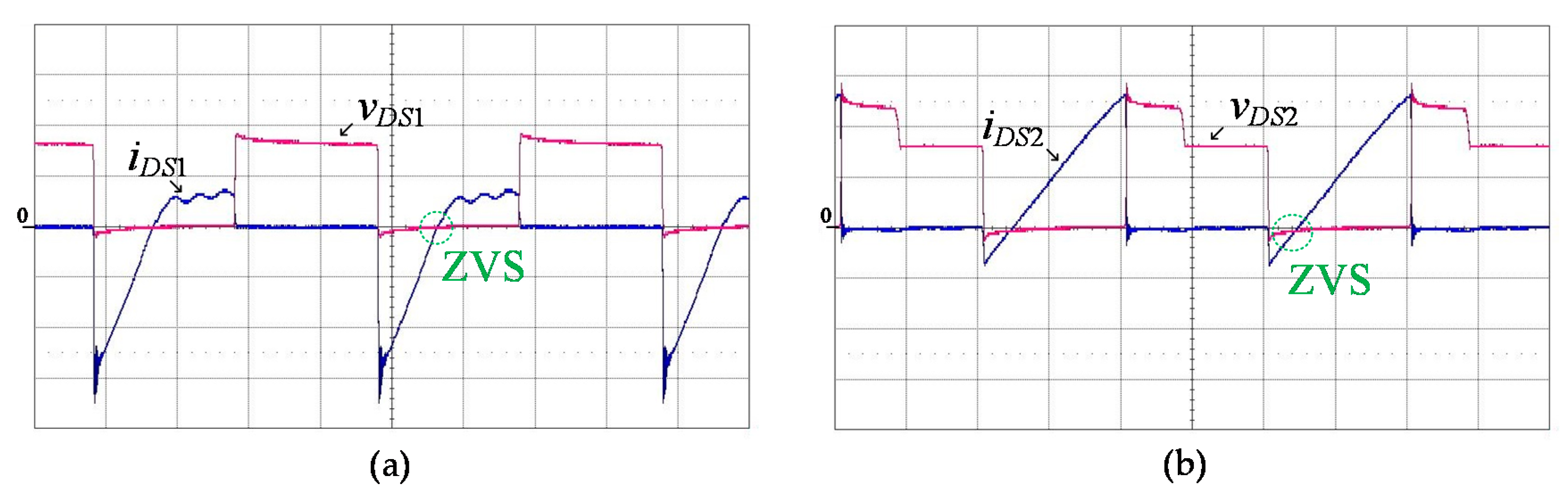
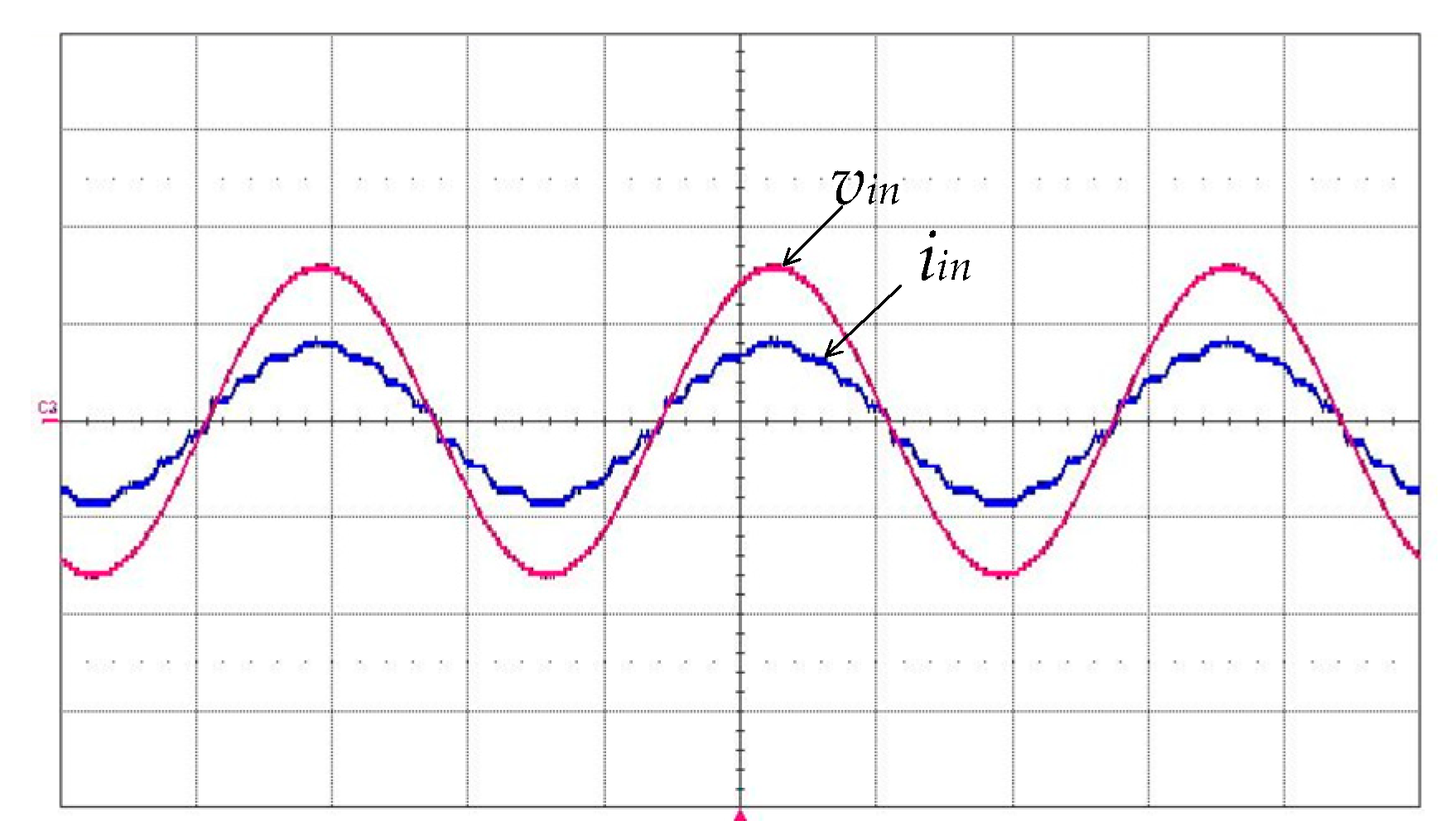
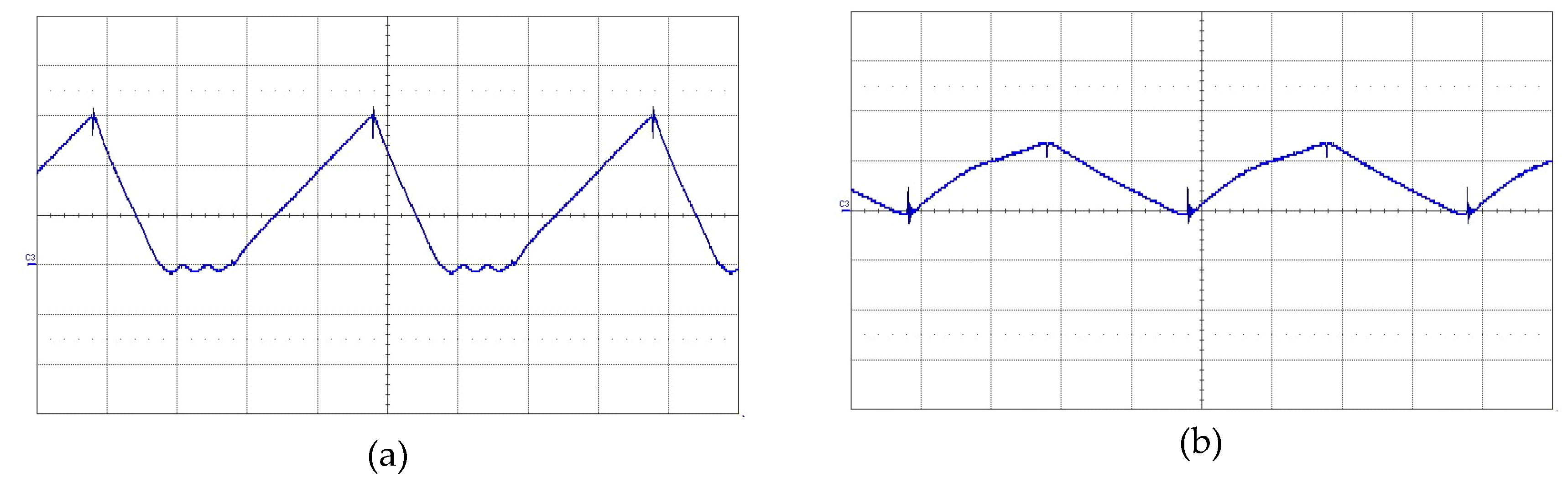
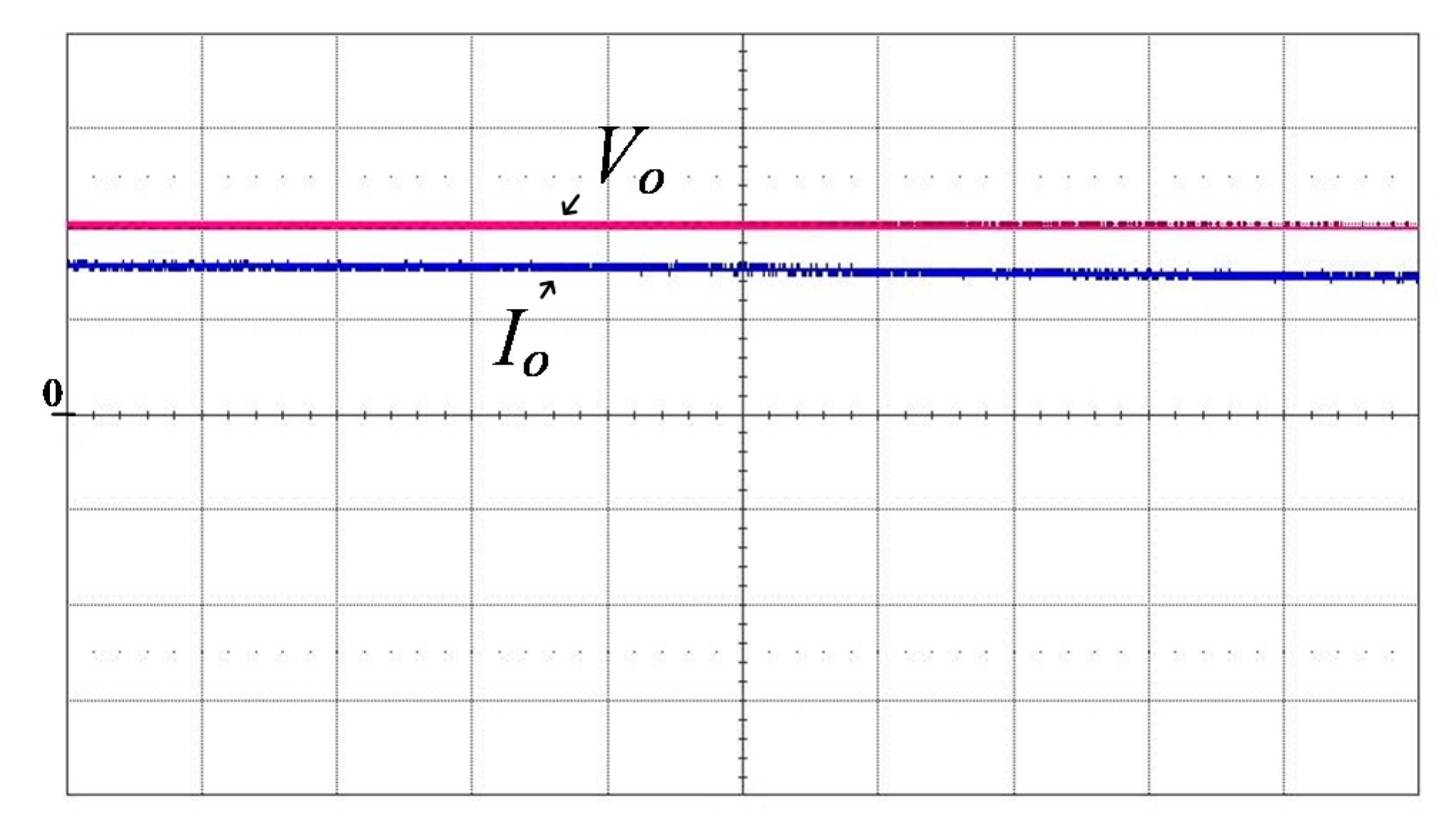
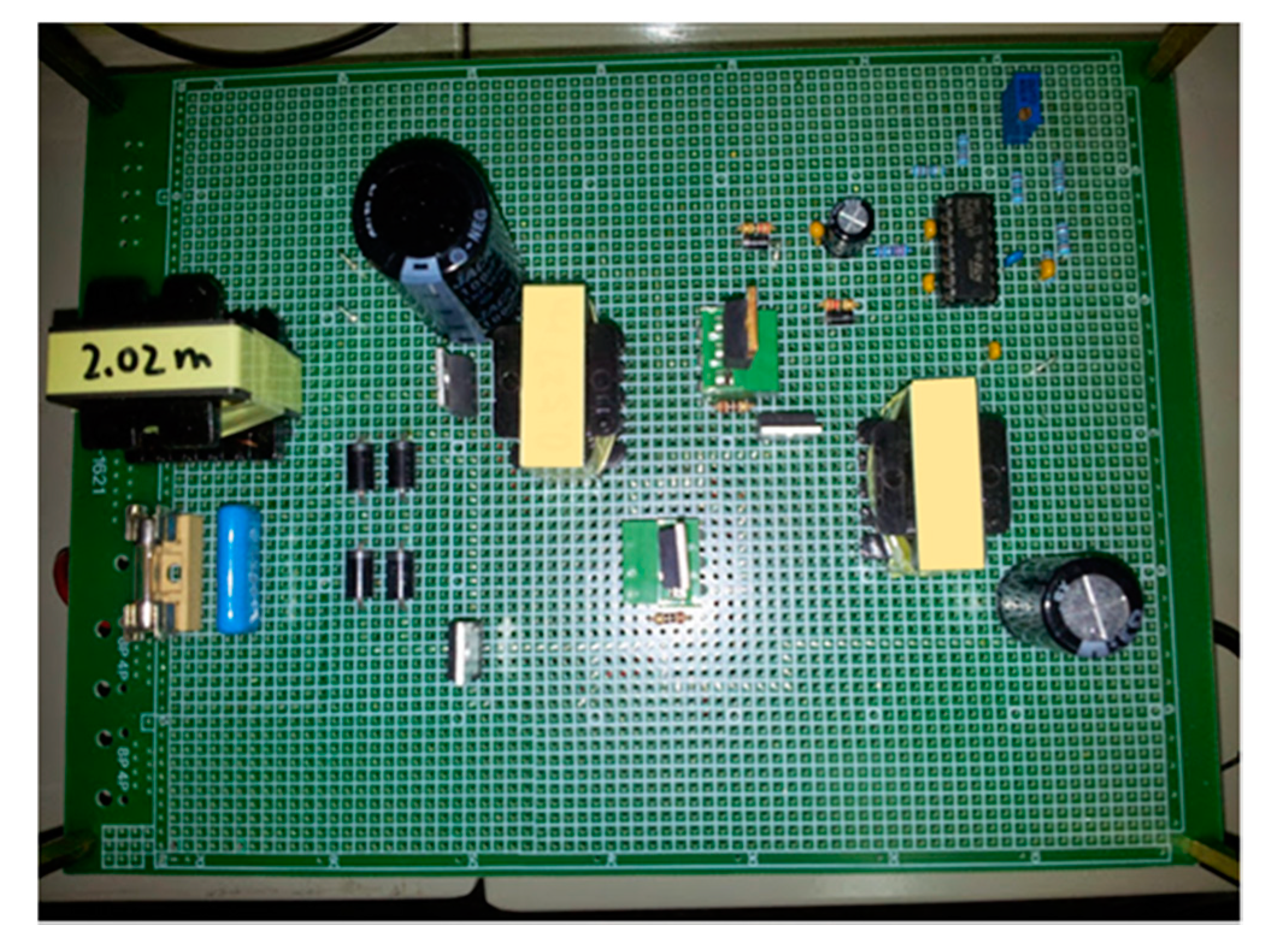
4.2. Experimental Results

From Equation (16), it is noted that the switching frequency is used to control the output power. As seen in Figure 2, the LED current is sensed by a series resistor Rs. The voltage across Rs which is proportional to the LED current is compared to a reference value Iref, and their difference is amplified by an operational amplifier in the error amplifier (EA). The output of the operation amplifier is sent to the half-bridge controller which mainly consists of a double-ended controller (L6599). The outputs of the half-bridge controller are two complementary waveforms (vGS1, vGS2) of which the frequency is regulated [12]. By this way, the switching frequency of the active switch is controlled to regulate the LED current. Figure 5 shows the measured waveforms of the input voltage and input current. The rms values of the input voltage and current are 112.4 V and 0.57 A, respectively. It can be observed that the input current is sinusoidal and in phase with the input voltage. The power quality in the input line is measured with a power analyzer (PowerLogic PM1000, Schneider Electric, Rueil-Malmaison, France). The measured PF is greater than 0.99, and the THDi is 3.5%. The inductor currents of both converters are shown in Figure 6 to indicate the DCM operation. There are spike currents in both the buck–boost inductor and the buck inductor. Theoretically, it is impossible to have a current spike in an inductor; otherwise, the voltage across the inductor would be tremendous high. The measured spike current in the buck–boost inductor and the buck inductor is believed to result from the interference voltage when one active switch is turned off. Figure 7 shows the waveforms of the output voltage and output current, which are well consistent with the design values. The DC values of the output voltage and current are 198.5 V and 0.304 A, respectively. In addition, the input power and output power are both measured with an oscilloscope. The measured values are 64 W and 60.3 W, respectively. The circuit efficiency is calculated to be 94.2%. Figure 8 shows waveforms of the voltage and current of the active switches. As shown, the switch current always increases from negative to positive. Its intrinsic diode conducts the negative current and clamps the switch voltage at almost zero volts. The active switch would naturally turn on as the switch current becomes positive, leading to ZVS operation. In the prototype circuit, MOSFET IRF840 serves the active switch. The current rating of the source-drain current (i.e., the current rating of the intrinsic diode) is 8 A maximum. It is seen in Figure 8, the maximum value of the diode current is about 3.5 A. Besides, the current in the intrinsic diode decreases linearly to zero. It means that the intrinsic diodes would turn off at zero current. Therefore, there is no faster diode in parallel with the active switch to replace the intrinsic diode. Figure 9 shows the prototype LED driver.

5. Conclusions

A novel AC/DC LED driver derived by integrating a buck–boost converter and a buck converter is proposed. The buck–boost converter serves as PFC converter to achieve high PF and low THDi while the buck converter steps down the DC-link voltage to drive high power white LEDs. A 60-W prototype circuit is built and tested to verify the theoretical analyses. Both the active switches can achieve ZVS. Experimental results show that the proposed circuit performs satisfactorily. A nearly unity PF (>0.99) and low THDi (3.5%) are achieved. With ZVS operation on both active power switches, the proposed circuit efficiency is as high as 94.2%.

Author Contributions

Y.-N.C. and H.-L.C. conceived and designed the circuit; C.-H.C. and H.-C.Y. performed circuit simulations and designed parameters of the circuit components; R.-Z.L. carried out the prototype LED driver, and measured as well as analyzed experimental results with the guidance from H.-L.C.; H.-L.C. wrote the paper and Y.-N.C. revised it for submission.

Acknowledgments

This work was supported by the Ministry of Science and Technology, R.O.C. under Grant MOST 104-2221-E-214-010.

Conflicts of Interest

The authors declare no conflict of interest.

References

  1. Ma, H.; Zheng, C.; Yu, W.; Gu, B.; Lai, J.S.; Feng, Q. Bridgeless electrolytic capacitor-less valley-fill AC/DC converter for offline twin-bus light-emitting diode lighting application. IET Power Electron. 2013, 6, 1132–1141. [Google Scholar] [CrossRef]
  2. Wang, Y.; Guan, Y.; Ren, K.; Wang, W.; Xu, D. A single-stage LED driver based on BCM boost circuit and LLC converter for street lighting system. IEEE Trans. Ind. Electron. 2015, 62, 5446–5457. [Google Scholar] [CrossRef]
  3. Wang, C.C.; Wu, K.H.; Liu, Y.C.; Yang, C.Y.; Alam, M.M.; Lo, Y.K.; Chiu, H.J. Study and implementation of an improved-power factor alternating-current light-emitting diode driver. IET Power Electron. 2015, 8, 1156–1163. [Google Scholar] [CrossRef]
  4. Wang, Y.; Huang, J.; Wang, W.; Xu, D. A single-stage single-switch LED driver based on class-E converter. IEEE Trans. Ind. 2016, 52, 2618–2626. [Google Scholar] [CrossRef]
  5. Gacio, D.; Alonso, J.M.; Calleja, A.J.; García, J.; Rico-Secades, M. A universal-input single-stage high-power-factor power supply for HB-LEDs based on integrated buck–flyback converter. IEEE Trans. Ind. Electron. 2011, 58, 589–599. [Google Scholar] [CrossRef]
  6. Xie, X.; Li, J.; Peng, K.; Zhao, C.; Lu, Q. Study on the single-stage forward-flyback PFC converter with QR control. IEEE Trans. Power Electron. 2016, 31, 430–442. [Google Scholar] [CrossRef]
  7. Fang, P.; Liu, Y.F.; Sen, P.C. A flicker-free single-stage offline LED driver with high power factor. IEEE J. Emerg. Sel. Top. Power Electron. 2015, 3, 654–665. [Google Scholar] [CrossRef]
  8. Weise, N.D.; Castelino, G.; Basu, K.; Mohan, N. A single-stage dual-active-bridge-based soft switched AC–DC converter with open-loop power factor correction and other advanced features. IEEE Trans. Power Electron. 2014, 29, 4007–4016. [Google Scholar] [CrossRef]
  9. Almeida, P.S.; Braga, H.A.C.; Dalla Costa, M.A.; Alonso, J.M. Offline soft-switched LED driver based on an integrated bridgeless boost–asymmetrical half-bridge converter. IEEE Trans. Ind. Appl. 2015, 51, 761–769. [Google Scholar] [CrossRef]
  10. Cheng, C.A.; Chang, C.H.; Chung, T.Y.; Yang, F.L. Design and implementation of a single-stage driver for supplying an LED street-lighting module with power factor corrections. IEEE Trans. Power Electron. 2015, 30, 956–966. [Google Scholar] [CrossRef]
  11. Cheng, H.L.; Lin, C.W. Design and implementation of a high-power-factor LED driver with zero-voltage switching-on characteristics. IEEE Trans. Power Electron. 2014, 31, 4949–4958. [Google Scholar] [CrossRef]
  12. Chang, C.H.; Cheng, C.A.; Chang, E.C.; Cheng, H.L.; Yang, B.E. An Integrated High-Power-Factor Converter with ZVS Transition. IEEE Trans. Power Electron. 2016, 31, 2362–2371. [Google Scholar] [CrossRef]
  13. Ma, H.; Lai, J.S.; Zheng, C.; Sun, P. A high-efficiency quasi-single-stage bridgeless electrolytic capacitor-free high-power AC–DC driver for supplying multiple LED strings in parallel. IEEE Trans. Power Electron. 2016, 31, 5825–5836. [Google Scholar] [CrossRef]
  14. Liu, K.H.; Lin, Y.L. Current waveform distortion in power factor correction circuits employing discontinuous-mode boost converters. In Proceedings of the 20th Annual IEEE Power Electronics Specialists Conference, Milwaukee, WI, USA, 26–29 June 1989; pp. 825–829. [Google Scholar]
  15. Cheng, H.L.; Hsieh, Y.C.; Lin, C.S. A novel single-stage high-power-factor AC/DC converter featuring high circuit efficiency. IEEE Trans. Ind. 2011, 58, 524–532. [Google Scholar] [CrossRef]
Figure 1. An integrated circuit with a boost converter and buck converter [12].
Applsci 08 00780 g001
Figure 2. Proposed AC/DC LED driver.
Applsci 08 00780 g002
Figure 3. Equivalent circuit of operation modes: (a) Modes I–(f) Modes VI.
Applsci 08 00780 g003
Figure 4. Theoretical waveforms.
Applsci 08 00780 g004
Figure 5. Waveforms of the input voltage and current. (vin: 100 V/div, iin: 1 A/div, time: 5 ms/div).
Applsci 08 00780 g005
Figure 6. Waveforms of inductor currents (a) Buck–boost inductor current ip (ip: 1 A/div, time: 5µs/div) and (b) Buck inductor current ib (ib: 0.5 A/div, time: 5 µs/div).
Applsci 08 00780 g006
Figure 7. Waveforms of Vo and Io. (Vo: 100 V/div, Io: 0.2 A/div, time: 5 ms/div).
Applsci 08 00780 g007
Figure 8. Waveforms of the voltages and currents of the active switches. (a) vDS1 and iS1 (vDS1: 200 V/div, iS1: 1 A/div, time: 5 µs/div) and (b) vDS2 and iS2 (vDS1: 200 V/div, iS1: 1 A/div, time: 5 µs/div).
Applsci 08 00780 g008
Figure 9. The prototype LED driver.
Applsci 08 00780 g009
Table 1. Specification of the proposed light-emitting diode (LED) driver.
Input voltage vin110 V ± 10% (rms), 60 Hz
Output power Po60 W
Output voltage Vo3.25 V × 60 = 195 V
Output Current Io0.308 A
Equivalent LED Resistance RLED633 Ω
Switching frequency fs50 kHz
Duty ratio D0.5
Table 2. Circuit parameters.
The low-pass inductance Lm 2.0 mH
The low-pass capacitance Cm0.47 μF
Dc-link capacitance Cdc100 μF
Output capacitance Co100 μF
Buck–boost inductor Lp0.47 mH
Buck inductor Lb2.26 mH
Active switches S1, S2IRF840
Diodes D1D7MUR460

