Article

Actively Controlling the Topological Transition of Dispersion Based on Electrically Controllable Metamaterials

Key Laboratory of Advanced Micro-structure Materials, MOE, School of Physics Science and Engineering, Tongji University, Shanghai 200092, China
*
Author to whom correspondence should be addressed.
Appl. Sci. 2018, 8(4), 596; https://doi.org/10.3390/app8040596
Submission received: 18 March 2018 / Revised: 4 April 2018 / Accepted: 4 April 2018 / Published: 10 April 2018
(This article belongs to the Section Optics and Lasers)

Abstract

:

Featured Application

Active optical devices.

Abstract

Topological transition of the iso-frequency contour (IFC) from a closed ellipsoid to an open hyperboloid provides unique capabilities for controlling the propagation of light. However, the ability to actively tune these effects remains elusive, and the related experimental observations are highly desirable. Here, a tunable electric IFC in a periodic structure composed of graphene/dielectric multilayers is investigated by tuning the chemical potential of the graphene layer. Specially, we present the actively controlled transportation in two kinds of anisotropic zero-index media containing perfect electric conductor/perfect magnetic conductor impurities. Finally, by adding variable capacitance diodes into a two-dimensional transmission-line system, we present an experimental demonstration of the actively controlled magnetic topological transition of dispersion based on electrically controllable metamaterials. With the increase in voltage, we measure the different emission patterns from a point source inside the structure and observe the phase-transition process of IFCs. The realization of an actively tuned topological transition will open up a new avenue in the dynamical control of metamaterials.

1. Introduction

Recently, hyperbolic metamaterials (HMMs) have attracted great attention due to their open iso-frequency contour (IFC) in the wave vector space. Once the topological transition from a closed ellipsoid to an open hyperboloid has been completed, the interaction between light and matter is significant changed, for example through enhanced spontaneous emission [1,2,3,4], all-angle negative refraction [5,6,7,8,9], super-resolution imaging [10,11,12,13,14], long-range interaction [15,16,17], nonlinear super-resolution imaging [18], and Cherenkov emissions with low energy electrons [19], etc. To date, by varying the frequency, the sign of the real part of permittivity ( ε ) or permeability ( μ ) in dispersive metamaterials is changed and thereby the topological transition of dispersion is realized [1,8,20,21]. In addition, by maintaining the real parts and tuning the imaginary part of ε or μ at a fixed frequency, the topological transition of the IFC has been theoretically analyzed [22] and experimentally demonstrated in metamaterials with added losses [23,24]. In contrast to the passive metamaterials, the study of actively tuned metamaterials and meta-devices is also an outstanding research topic [25,26,27,28]. Actively controlled metamaterial systems have been predicted to be able to yield new applications ranging from electrically switchable devices [27] to tunable coupling devices [26,28]. The realization of the actively tunable topological transition of the IFC is also very useful in the design of new active optical devices. To realize the externally tunable behaviors, two-dimensional (2D) semiconductors such as graphene are usually utilized. Graphene, a 2D honeycomb lattice of carbon atoms, is electrically characterized by its surface conductivity σ ( ω , μ c ) , where μ c is the chemical potential that can be tuned by the gate voltage [25], and ω denotes the angular frequency. Tunable absorption [29,30], giant Purcell effect [31], tunable invisibility cloaking of particles by means of graphene coatings [32,33], and hyperbolic plasmonics [34,35] have been theoretically proposed in graphene-based structures associated with the hyperbolic property in suitable conditions. In this paper, by tuning the chemical potential of the graphene layer, we theoretically analyze and numerically simulate the tunable emission patterns in a periodic structure composed of graphene/dielectric multilayers. The emission patterns clearly show the topological transition of the IFC from a closed ellipsoid to an open hyperboloid [20,24]. Remarkably, by actively changing the chemical potential of the graphene layer, two special cases corresponding to two kinds of anisotropic ε -near-zero (ENZ) media can be realized in the proposed structure at a fixed frequency. To observe the influence of the topological transition on the wave propagations, we study the transmission property of the two kinds of ENZ media embedded with a perfect electric conductor (PEC) or perfect magnetic conductor (PMC) defect. Furthermore, we propose a microwave experimental platform to demonstrate the actively controlled topological transition of the IFC. By adding electrically controlled diodes into a two-dimensional (2D) transmission line (TL) system, we experimentally observe the actively tuned topological transition from the emission patterns by modulating the external voltages applied in the diodes.
The paper is organized as follows. In Section 2, by tuning the chemical potential of graphene layer, we show an actively adjustable topological transition of dispersion in the periodic structure composed of graphene and dielectric layers. Moreover, the influences of the topological transition of dispersion on the scattering properties of structures with embedded PEC or PMC defects have been fully studied. Then, in Section 3, based on a 2D TL system, we experimentally demonstrate the actively controlled topological transition of dispersion based on electrically controllable metamaterials. Finally, we conclude in Section 4.

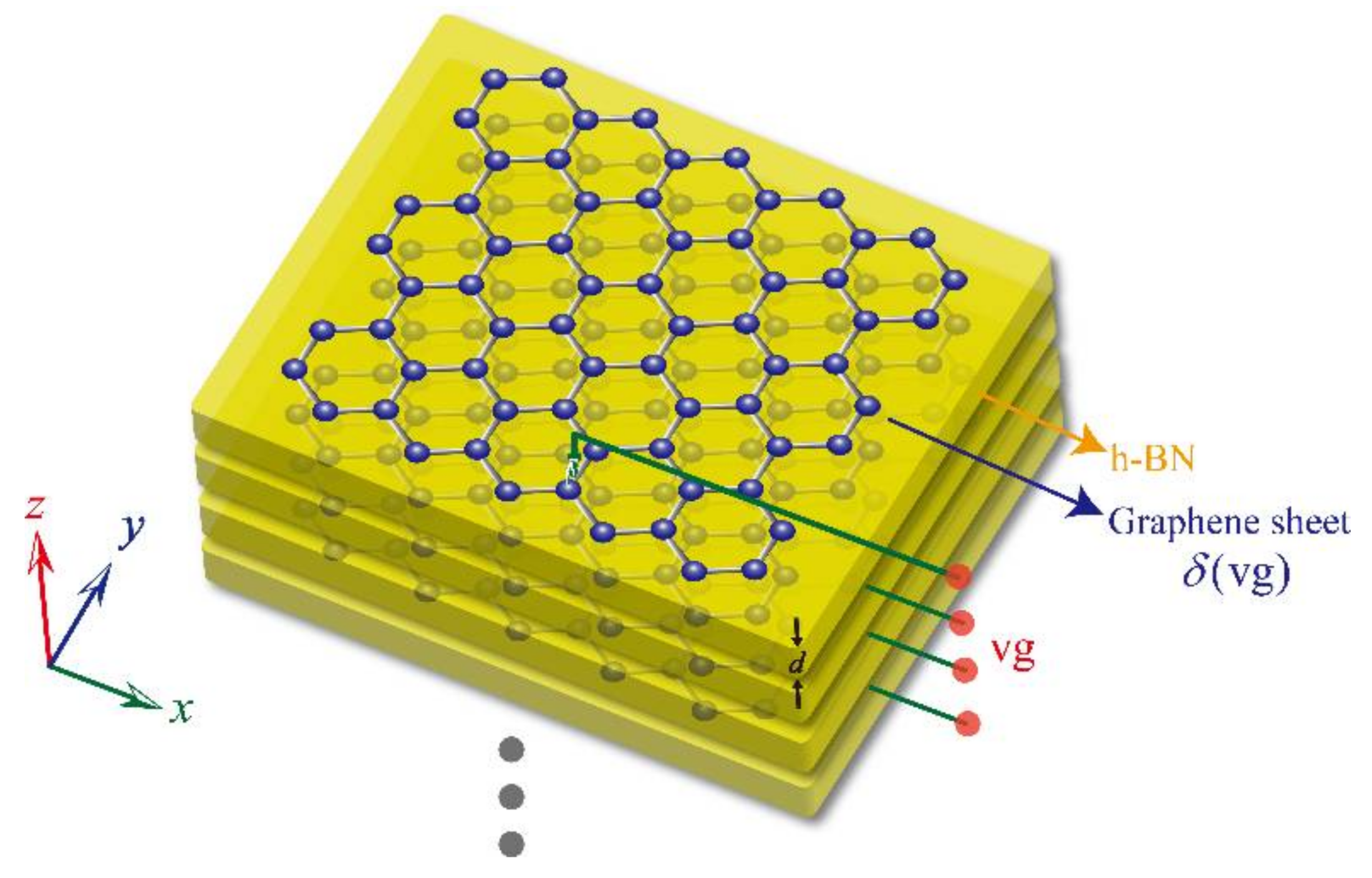
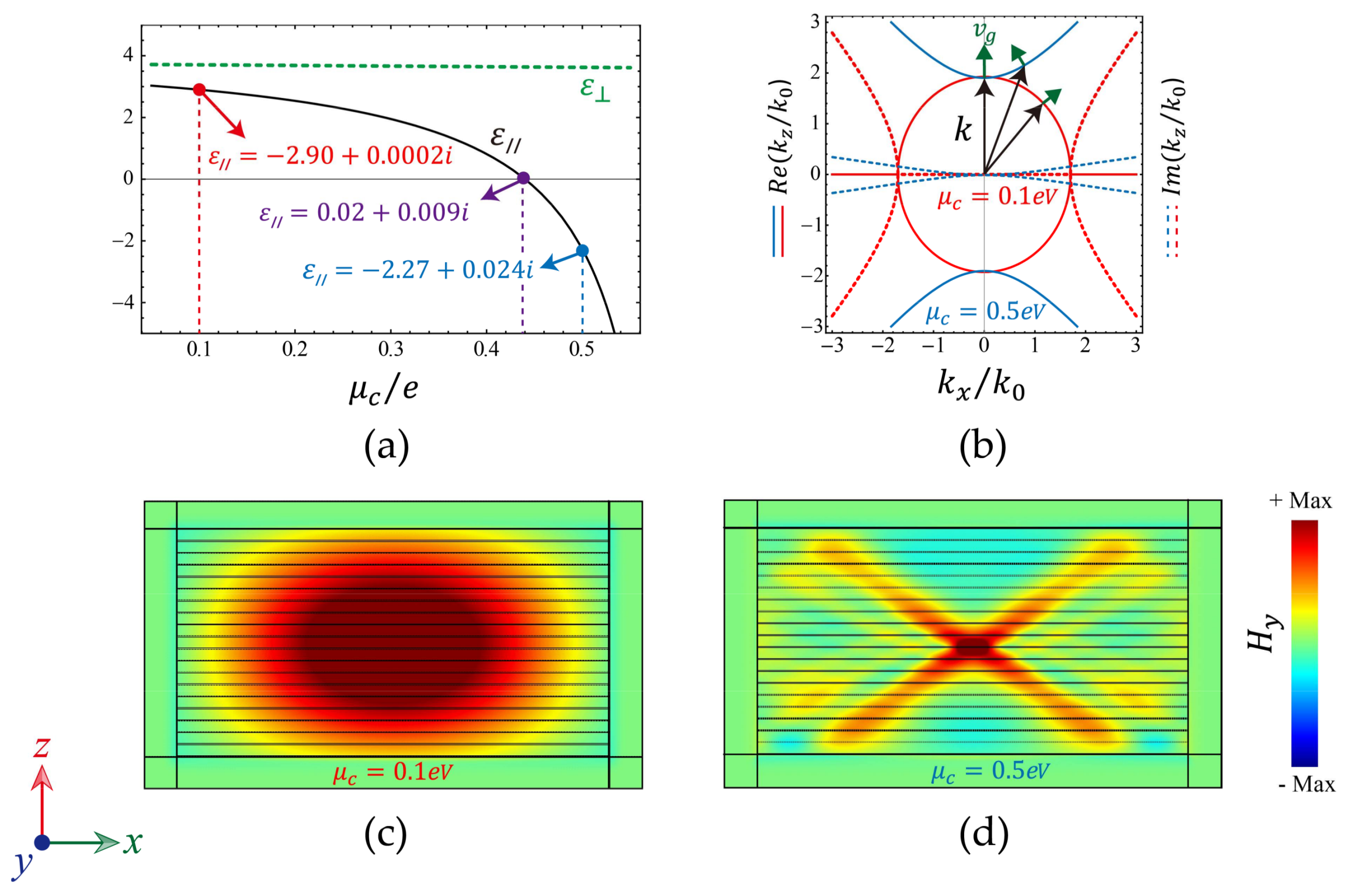
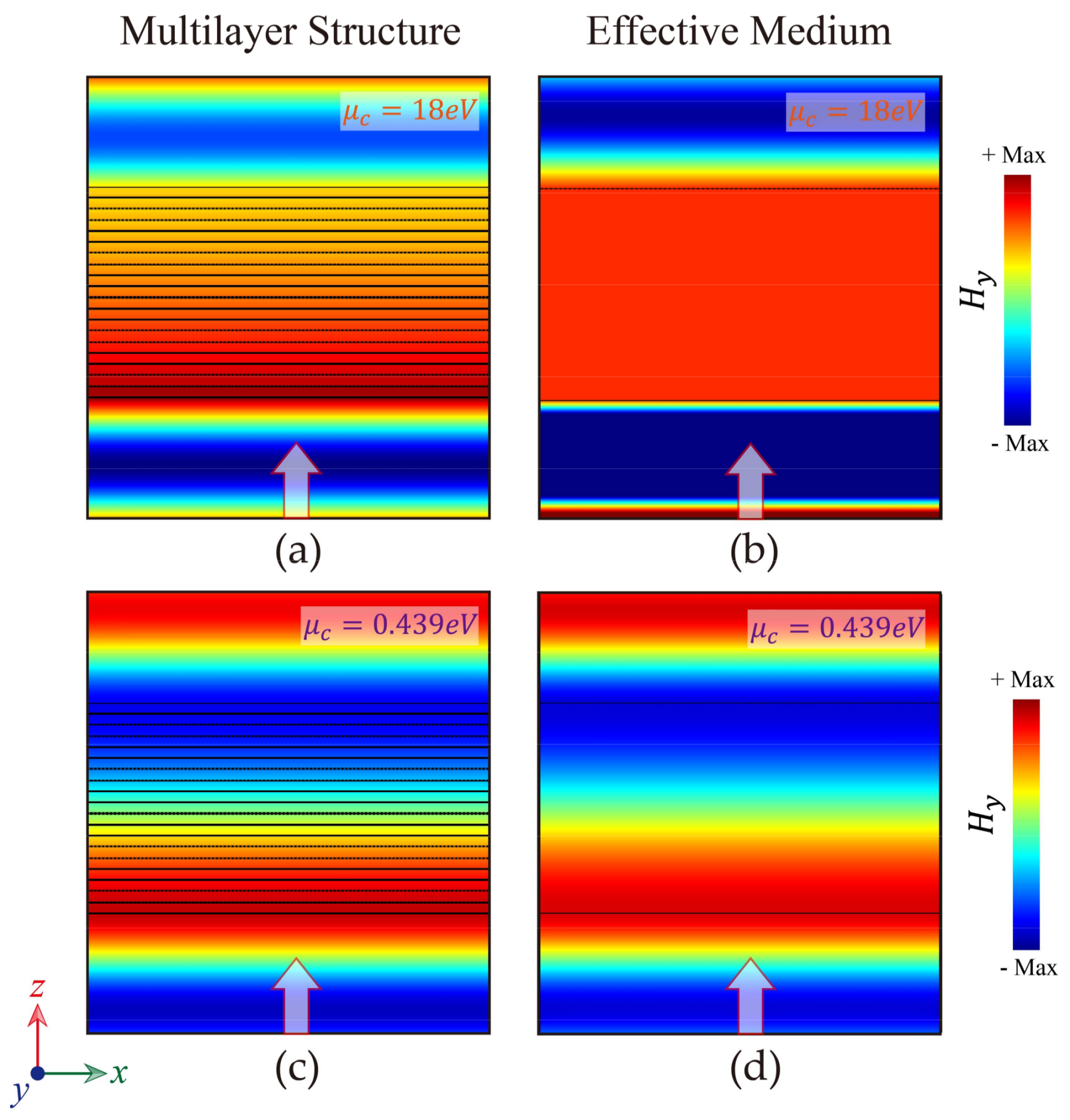
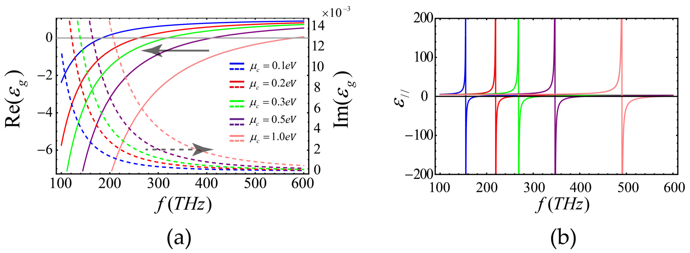
2. Actively Tunable Topological Transition in Graphene/Dielectric Multilayers

Voltage-controlled topological transition of dispersion can be realized by actively tuning the anisotropic parameters of permittivity or permeability. In this section, based on the multilayers composed of graphene and a dielectric, we theoretically study the voltage-controlled topological transition by varying the permittivity. Then, owing to the difficulty of related experiments, we experimentally demonstrate the voltage-controlled topological transition by varying the permeability in the microwave regime in Section 3.
We consider the structure, shown in Figure 1, which is composed of graphene layers separated by dielectric slabs. For the graphene sheet, its electromagnetic properties are characterized by the surface conductivity σ ( ω , μ c ) . The σ ( ω , μ c ) can be calculated using the Kubo formula [36,37]:
σ ( ω , μ c ) = σ int r a ( ω , μ c ) + σ int e r ( ω , μ c ) ,
Here, σ int r a ( ω , μ c ) and σ int e r ( ω , μ c ) denote the conductivity due to the intra-band and inter-band contribution, respectively.
σ int r a ( ω , μ c ) = i e 2 π 2 ( ω + i τ 1 ) [ 0 p ( f d ( p ) p f d ( p ) p ) d p ] σ int e r ( ω , μ c ) = i e 2 ( ω + i Γ ) π 2 [ 0 f d ( p ) f d ( p ) ( ω + i τ 1 ) 2 4 ( p / ) 2 d p ] ,
where f d ( p ) is the Fermi–Dirac distribution function: f c ( p ) = { 1 + exp [ ( p μ c ) / ( k B T ) ] } 1 , k B , ω , , e , T , and τ 1 are the Boltzmann’s constant, angular frequency, Planck constant, charge of an electron, temperature, and collision rate, respectively. τ 1 = 10 12 is assumed independent of the energy p . μ c is the chemical potential that can be tuned by the external voltage v g [25]. At high frequencies, the contribution from the inter-band can be neglected. For the Fermi–Dirac statistics, conductivity can be simplified as [36]:
σ ( ω , μ c ) = i e 2 μ c π 2 ( ω + i τ 1 ) .
When electronic band structure of a graphene sheet is unaffected by the neighboring layers, the effective permittivity of graphene can be calculated as follows [25]:
ε g = 1 + i σ ( ω , μ c ) / ε 0 ω t g ,
where t g = 1 nm and ε 0 are the thickness of graphene and the permittivity of the vacuum, respectively. For the varied chemical potential μ c , the different effective complex permittivity values of graphene based on Equation (4) are shown in Figure 2a. The real and imaginary parts of ε g are marked by solid and dashed lines, respectively. We can clearly find that the complex value of ε g is sensitive to the value of μ c , and the real part of ε g has a redshift with the μ c value increased. Owning to the flexibly regulated ε g , the active topological transition of dispersion can be easily realized. Considering the graphene/dielectric multilayer structure, the components of the effective dielectric permittivity tensor parallel ( ε / / ) and perpendicular ( ε ) to the anisotropic axis are given by the effective medium theory [38]:
ε / / = t g + t d t g / ε g + t g / ε g , ε = ε g t g + ε d t d t g + t d ,
where t d = 10 nm and ε d = 4 are the thickness and permittivity, respectively, of the dielectric layer for hexagonal boron-nitride (h-BN) [30,39]. According to Equation (5), the value and the sign of ε / / can be flexibly adjusted by changing the value of μ c , as shown in Figure 2b. Considering a fixed frequency f = 385 THz, when the value of μ c increases from 0.1 eV to 0.5 eV, the sign of ε / / reverses at the critical point 0.439 eV, while the sign of ε remains positive, as displayed in Figure 3a.
Considering the light with transverse magnetic (TM) ( H y , E x , E z ) polarization propagating in the x-z plane of the 2D uniaxial media, the IFC in such a strongly anisotropic metamaterial is given by [12]:
k x 2 ε / / + k z 2 ε = μ / / k 0 2 ,
where k x and k z are the x and z components of the wave vector, respectively. k 0 = ω / c is the vector in free space. c is speed of light and μ / / is the effective magnetic permeability. The IFC in the wave-vector space ( k x k z ) can be obtained according to Equation (6). In the low chemical potential case μ c = 0.1 eV, at f = 385 THz the IFC is a closed ellipsoid, and is shown by a red line in Figure 3b.
The solid (dashed) lines give the relationship of Re ( k z ) ( Im ( k z ) ) with k x . By using COMSOL MULTI-PHYSICS, the emission pattern of the ellipsoid IFC is shown in Figure 3c (see Appendix A for details of the simulations). In the simulation, a current source is put at the center of the material. However, when the chemical potential is changed to μ c = 0.5 eV, the IFC of the graphene/dielectric multilayers will be in the form of a hyperbola, which is marked by the solid blue line in Figure 3b. The change of the IFC will strongly modify the propagation and emission properties of electromagnetic waves. The emission pattern is an open line because the density of states is at a maximum along the hyperbolic asymptote (Figure 3d) [40]. The chemical potential of graphene is modulated by an applied electric field and the topological transition of dispersion is realized with the changed chemical potential [25,26,27,28,29,30,31,32,33,34,35]. This actively controlled topological transition will greatly change the emission pattern of a source in the medium. From the simulated emission patterns, we can find that the emission patterns as shown in Figure 3c,d coincide with the IFCs based on the effective medium theory (Figure 3b). Hence, the actively tunable IFCs in graphene/dielectric multilayers are realized by tuning the chemical potential of graphene layer.
We further study the influences of the topological transition of dispersion on the scattering properties of structures if the PEC or PMC defect is added. According to Equation (5), the sign of ε also can be controlled with the varied μ c , which is shown in Figure 4a. The effective parameters of ε and ε / / are marked by green dashed line and black line, respectively. We can clearly see that the sign of ε will change at the critical point 18 eV as the value of μ c increases. At the critical state μ c = 18 eV, the IFC is a very flat elliptic curve along the horizontal direction (marked by orange line in Figure 4b), which can be regarded as one kind of anisotropic ENZ medium. As another kind of anisotropic ENZ medium for μ c = 0.439 eV in Figure 3a, the IFC is a very flat elliptic curve along vertical direction (marked by a purple line in Figure 4b). So far, based on a passive system, unusual transportation properties of the light in anisotropic ENZ metamaterials have been demonstrated, including collimation [41], flux manipulation [42], and total transmission (reflection) [43]. Now, with the aid of active control, we study the actively tuned transmissions of two kinds of anisotropic ENZ media based on the graphene/dielectric multilayers. For a type I anisotropic ENZ medium ( μ c = 18 eV), when a plane wave is incident on this structure embedded with a tiny PEC defect, the wave can perfectly pass through this defect without any influence, as is shown in Figure 4c. The transmission behavior will change once the PEC defect is replaced by a PMC defect and the incident wave will be scattered by the defect (Figure 4d). Similar to the type I anisotropic ENZ medium, for the type II anisotropic ENZ medium ( μ c = 0.439 eV), Figure 4e shows that the incident wave also will not be affected by the PEC defect, as in the case of Figure 4c. However, the transmission will dramatically change for the structure containing a PMC defect. In this case, the incident wave will be completely blocked by the tiny defect (Figure 4f), which is similar to the total reflection effect realized in the double near-zero index material [44]. So, inspired by the demonstration of the topological transition of dispersion, we present the novel transportation behavior that can be controlled in an active manner.

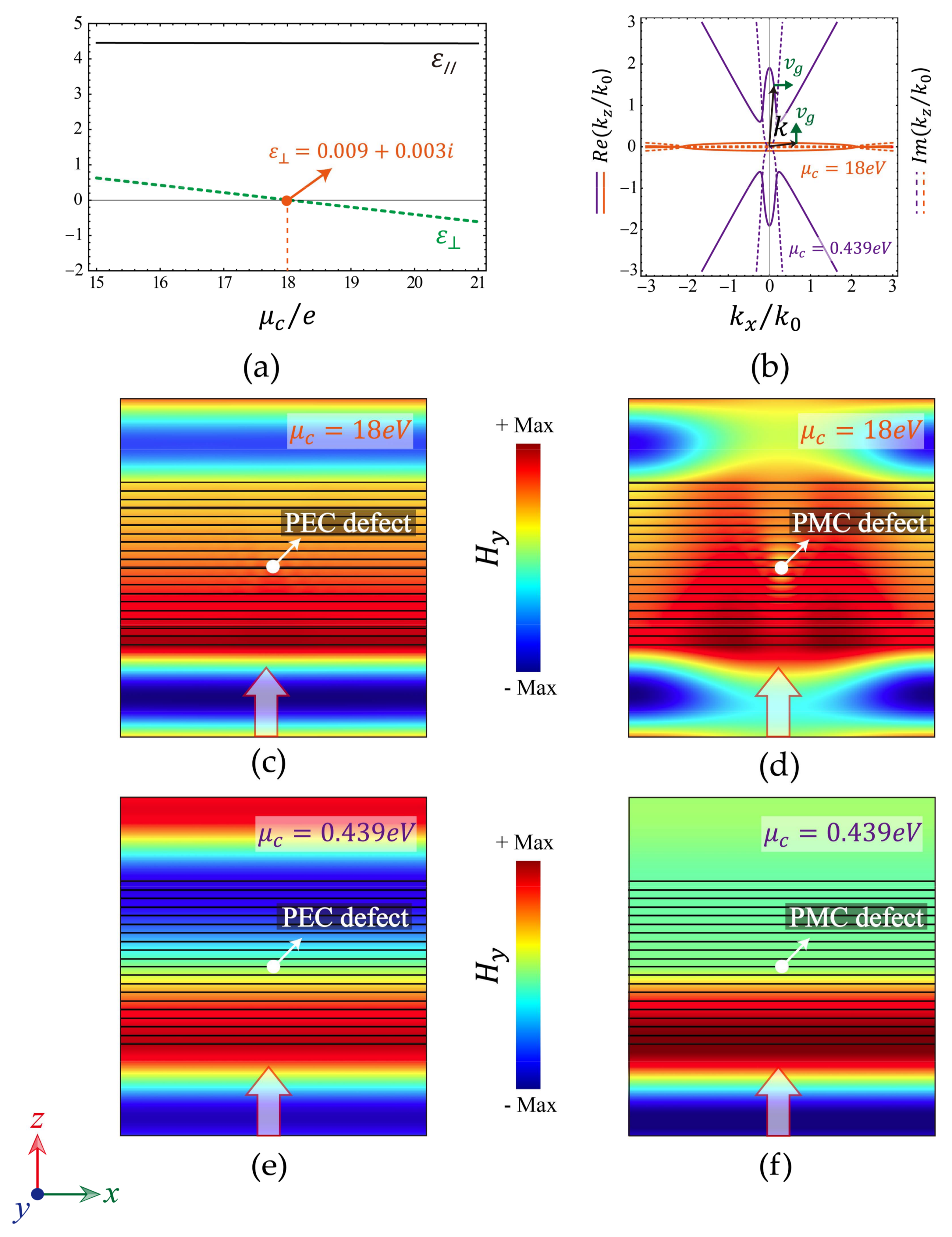
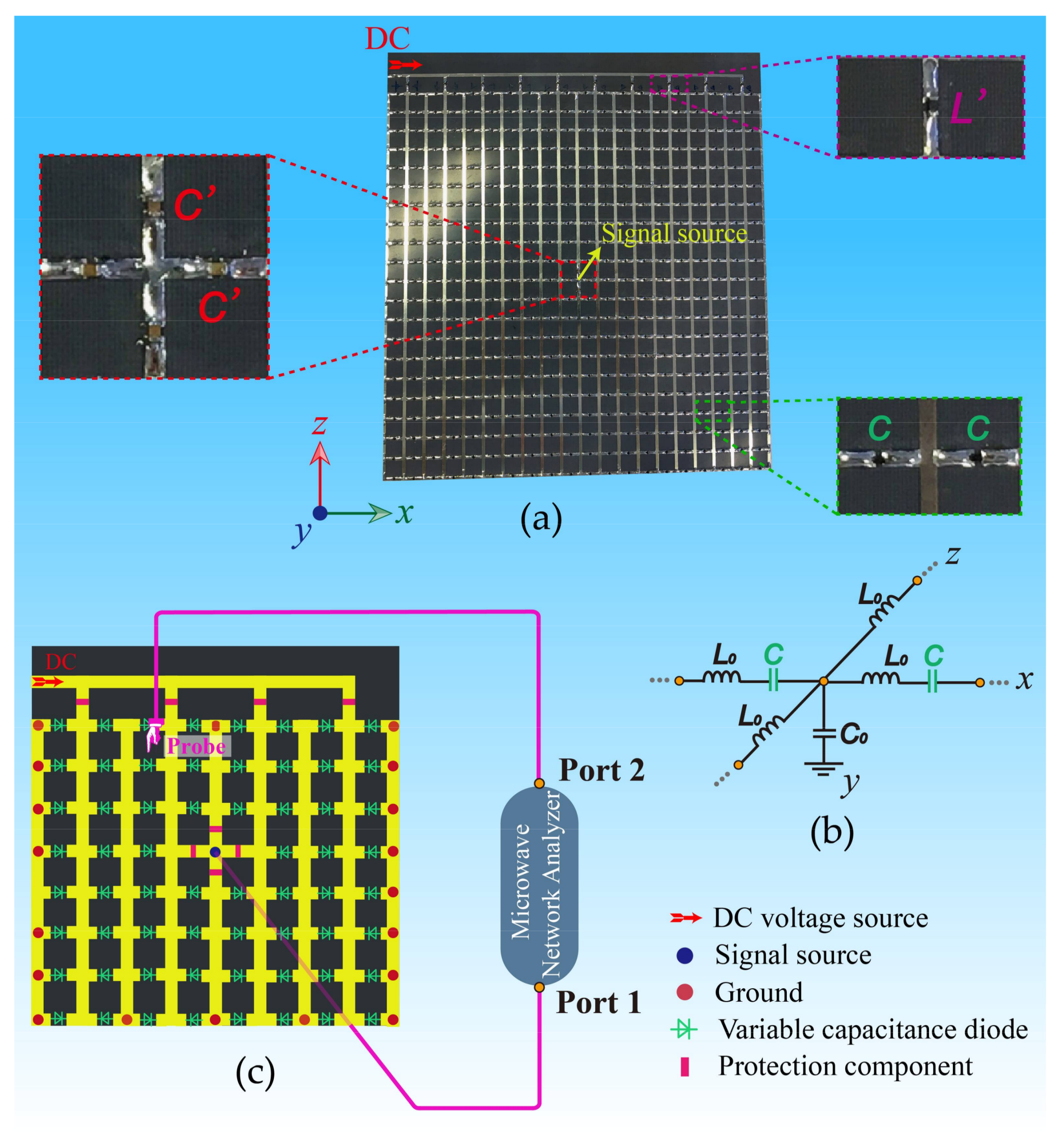
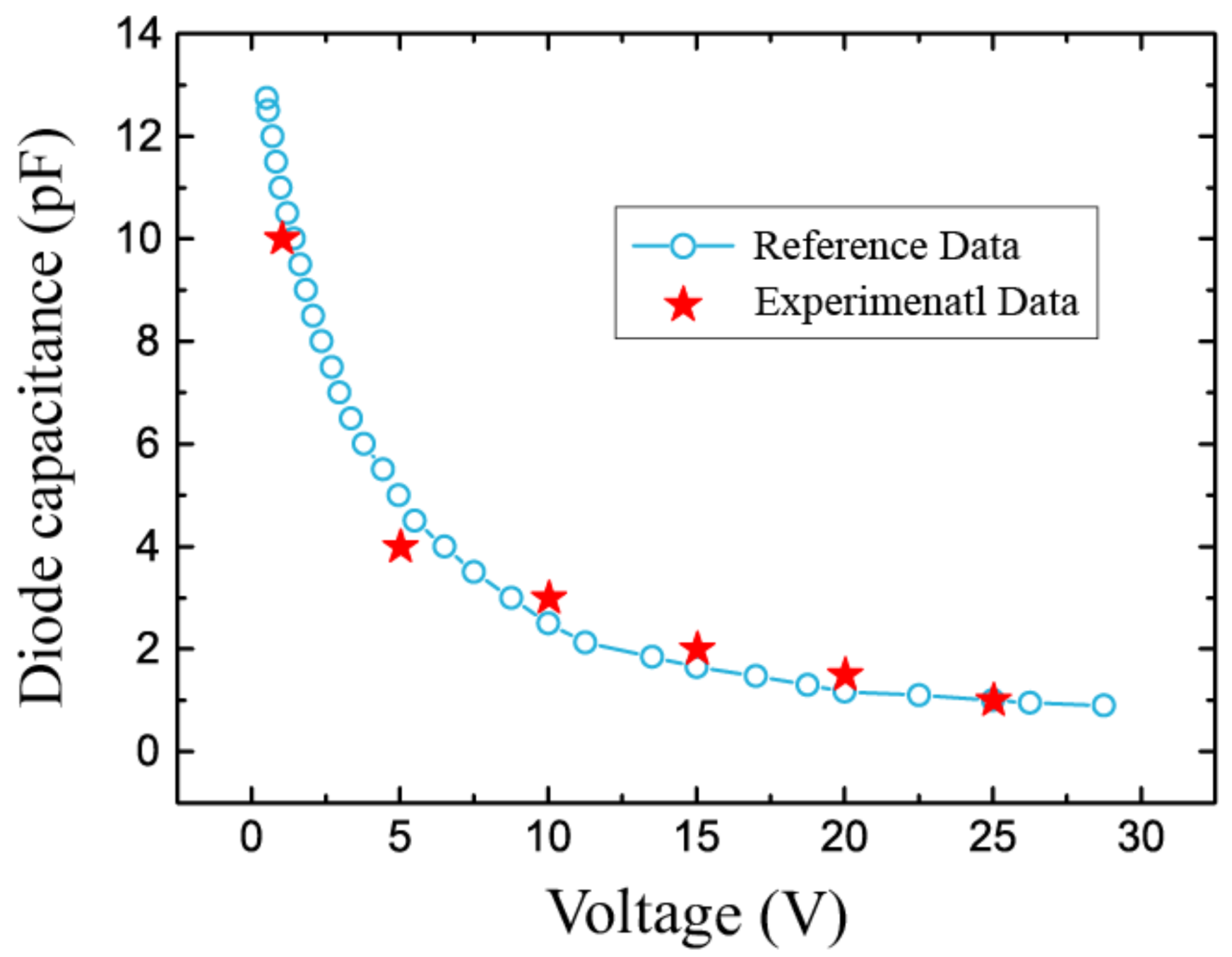
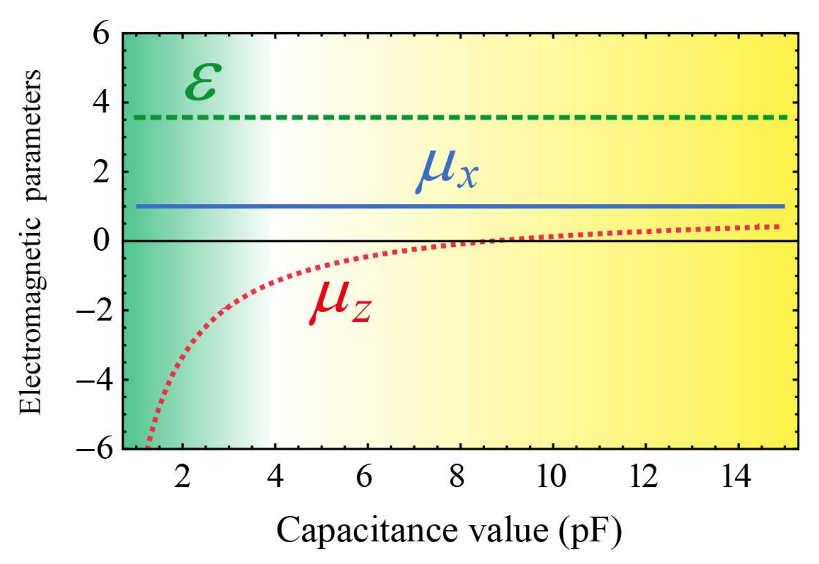
3. Experimental Demonstration of the Actively Tunable Topological Transition Based on TLs

In the visible range, the experimental realization of the actively tunable topological transition of dispersion is still a great challenge. For example, in Figure 1, besides the difficulty in fabricating the multilayers, it is not easy to precisely add the same external voltage to each graphene layer. In this section, we introduce a microwave platform based on 2D TLs to experimentally demonstrate the actively controlled topological transition. The experimental schematic of the TL-based metamaterial is shown in Figure 5a and the corresponding circuit model is shown in Figure 5b. The insets near Figure 5a show the enlarged lumped variable capacitance diodes and the protected elements, respectively. Figure 5c shows the schematic of the experimental platform to realize the actively control topological transition. For better visibility, the number of the unit cell ( 8 × 8 ) in Figure 5c is smaller than the experimental sample ( 20 × 20 ) in Figure 5a. In the experiment, a direct voltage source is connected to the sample from the top, which is marked by the red arrow. The grounding position is indicated by red dots. The signal is input at the center of the sample and the protection component is added to avoid the interaction between direct current (DC) source and the signal source, as is shown in Figure 5c.
Here, our sample is composed of 20 × 20 unit cells with lumped elements that are fabricated on a commercial printed circuit board, F4B, with a relative permittivity of ε r = 2.2 and thickness of h = 1.6 mm. The width of the micro-strip lines is w = 2 mm. The unit lengths of TL in the x and z direction are d = 12 mm. The structural factor of the TL is defined as g = Z 0 / η e f f , where Z 0 and η e f f are the characteristic impedance and the effective wave impedance of the normal TL, respectively. When w > h , the structural factor g = [ 1.393 + w / h + 0.667 ln ( w / h + 1.444 ) ] 1 0.303 . Then, we load elements into the normal TL to realize the tunable metamaterials. Considering the transverse electric (TE) wave ( E y , H x , H z ), According to the quasi-static TE polarized solution and Ampere’s law, by loading the variable capacitance diode C , the effective permittivity and permeability of 2D TLs in the long-wavelength limit can be written as [23,45]:
ε = 2 C 0 g / ε 0 , μ x = L 0 / ( p μ 0 ) , μ z = ( L 0 g 1 ω 2 C d g ) / μ 0 , ,
where μ 0 is permeability of vacuum. L 0 and C 0 are the per-unit-length inductance and capacitance of TL segment, respectively. The effective permittivity ε 3.57 is isotropic in our structure. For the varactors, one can change the external voltage to tune the capacitance value of C . The reference relationship between bias voltage and the diode capacitance provided by the product manual is indicated by the blue dotted line in Figure 6. From Equation (7), by continuously changing the value of C , the sign and value of μ z can be actively controlled at a fixed frequency. Through the modulation of capacitance, we can manipulate the sign of μ z from negative to positive while the signs of ε and μ x remain positive, as shown in Figure 6.
The 2D TLs can be described by the effective medium theory and the dispersion relation is derived as [2,17]:
k x 2 μ z + k z 2 μ x = ε k 0 2 .
Based on Equation (8), we calculate different IFCs by varying the value of C at 0.8 GHz, as is shown in Figure 7a. One can see that the topological transition of IFC will happen once the value of C changes from 10 pF to 4 pF. Moreover, the IFC will become more and more flat with the decrease of C .
We further use the computer simulation technology (CST) microwave studio software to perform the simulation. A linearly polarized source is loaded near the center of the sample, as is marked by the blue point in Figure 5. In Figure 7b, we simulated E y patterns of sample at 0.8 GHz by varying the value of C . The emission patterns for different values of C coincide well with the IFCs in Figure 7a. For example, for C = 10 pF, the IFC is a closed ellipsoid and the source can propagate in all in-plane directions. However, for C = 4.0 pF, the IFC is an open hyperbolic curve and the source can only propagate in some directions. In particular, for C = 1.0 pF, the IFC is very flat. The source is collimated and can only propagate in the vertical direction.
Now we perform an experiment to observe the emission patterns. In the experiment, a DC voltage source is connected to the sample from the top, which is marked by the red arrow in Figure 5. With the increase of the voltage, we measure the different emission patterns at 0.8 GHz to observe the changing process of IFCs (see Appendix B for the details of experimental operation). The measured E y patterns in Figure 7c agree well with the numerically simulated one in Figure 7b. Hence, based on 2D TLs, we have experimentally demonstrated the actively controlled magnetic topological transition of dispersion by changing the external voltages.

4. Conclusions

In conclusion, we demonstrate the actively tuned topological transition of dispersion in graphene/dielectric multilayers and the influence on the scattering properties when a PEC or PMC defect is embedded in the structure. Moreover, based on 2D TLs loaded with lumped variable capacitance diodes, we experimentally realize the actively controlled topological transition of dispersion. Our results represent a step towards the active control of wave propagations based on metamaterials.

Acknowledgments

This work is supported by the National Key R & D Program of China (No. 2016YFA0301101); by the National Nature Science Foundation of China (NSFC) (Grant Nos. 11774261, 11474220, and 61621001); and the Science Foundation of Shanghai (No. 17ZR1443800).

Author Contributions

Zhiwei Guo conducted the theoretical calculations and carried out the experimental measurements. Yong Sun and Yunhui Li suggested the approach. Haitao Jiang and Hong Chen supervised the whole work. All authors reviewed the paper.

Conflicts of Interest

The authors declare no conflict of interest.

Appendix A. Simulation Method about the Details of the COMSOL Simulation

The field distributions of the multilayer structure composed of graphene and h-BN are numerically calculated by the software COMSOL, which is based on the finite-element method. Specifically, a perfectly matched layer around the material is used to avoid the boundary reflection in Figure 3. Furthermore, in our paper we consider a 2D structure where the y direction is regarded as infinity. So, the surfaces of H y shown in Figure 3c,d are same for any cross section along the y direction.
Specifically, in order to better guide the reader, the results of the nonlocal model (multilayer structure) and the local model (effective structure) have been compared in this part. The results of effective structure (Figure A1b,d) agree well with the results of the multilayer structure (Figure A1b,d). So, the effective medium theory works well here.
Figure A1. When μ c = 18 eV, the magnetic field distribution H y of the multilayer structure and effective medium are shown in (a,b), respectively. (c,d) Similar to (a,b), but μ c is changed to 0.439 eV. The arrow identifies the direction of the incident light.
Applsci 08 00596 g0a1

Appendix B. Details of the Experimental Methods

In our experiment, Philips BB181 is used as the variable capacitance diode (marked by green color for see). In order to compare with the simulations, we take a series of voltage values, 1 V, 5 V, 10 V, 15 V, 20 V, and 25 V, respectively. The experimental data on the relationship between the used voltage and the diode capacitance is displayed by the red stars in Figure A2. It is seen that the experimental data coincides well with the reference data.
Figure A2. Diode capacitance as a function of bias voltage. Blue dotted line and the red stars are the reference data and experimental data, respectively.
Applsci 08 00596 g0a2
Under the proper design of the shunt connection, the voltage of all the variable capacitance diodes is nearly the same. The signal is emitted from port one of vector network analyzer (Agilent PNA Network Analyzer N5222A) and the electric fields E y are measured by another antenna (i.e., near-filed probe) connecting to port 2 of the network analyzer. The near-field probe is vertically placed 1 mm above the TLs to measure the signals of electric fields of the TLs. In order to accurately probe the field distributions in the near-field scanning measurement, our experimental sample is placed on an automatic translation device. The spatial step of scanning the near field is set to be 1 mm in the x and y directions, respectively.

References

  1. Krishnamoorthy, H.N.; Jacob, Z.; Narimanov, E.; Kretzschmar, I.; Menon, V.M. Topological transitions in metamaterials. Science 2012, 336, 205–209. [Google Scholar] [CrossRef] [PubMed]
  2. Kruk, S.S.; Wong, Z.J.; Pshenay-Severin, E.; O’Brien, K.; Neshev, D.N.; Kivshar, Y.S.; Zhang, X. Magnetic hyperbolic optical metamaterials. Nat. Commun. 2016, 7, 11329. [Google Scholar] [CrossRef] [PubMed]
  3. Schulz, K.M.; Vu, H.; Schwaiger, S.; Rottler, A.; Korm, T.; Sonnenberg, D.; Kipp, T.; Mendach, S. Controlling the spontaneous emission rate of quantum wells in rolled-up hyperbolic metamaterials. Phys. Rev. Lett. 2016, 117, 085503. [Google Scholar] [CrossRef] [PubMed]
  4. Galfsky, T.; Gu, J.; Narimonov, E.E.; Menon, V.M. Photonic hypercrystals for control of light–matter interactions. Proc. Natl. Acad. Sci. USA 2017, 114, 5125–5129. [Google Scholar] [CrossRef] [PubMed]
  5. Fang, A.; Koschny, T.; Soukoulis, C.M. Optical anisotropic metamaterials: Negative refraction and focusing. Phys. Rev. B 2009, 90, 115155. [Google Scholar] [CrossRef]
  6. Naik, G.V.; Liu, J.; Kildishev, A.V.; Shalaev, V.M.; Boltasseva, A. Demonstration of Al: ZnO as a plasmonic component for near-infrared metamaterials. Proc. Natl. Acad. Sci. USA 2012, 109, 8834–8838. [Google Scholar] [CrossRef] [PubMed]
  7. Argyropoulos, C.; Estakhri, N.M.; Monticone, F.; Alù, A. Negative refraction, gain and nonlinear effects in hyperbolic metamaterials. Opt. Express 2013, 21, 15037–15047. [Google Scholar] [CrossRef] [PubMed]
  8. High, A.A.; Devlin, R.C.; Dibos, A.; Polking, M.; Wild, D.S.; Perczel, J.; de Leon, N.P.; Lukin, M.D.; Park, H. Visible-frequency hyperbolic metasurface. Nature 2015, 522, 192–196. [Google Scholar] [CrossRef] [PubMed]
  9. Zhang, R.Z.; Zhang, Z.M. Tunable positive and negative refraction of infrared radiation in graphene-dielectric multilayers. Appl. Phys. Lett. 2015, 107, 191112. [Google Scholar] [CrossRef]
  10. Jacob, Z.; Alekseyev, L.V.; Narimanov, E.E. Optical hyperlens: Far-field imaging beyond the diffraction limit. Opt. Express 2006, 14, 8247–8256. [Google Scholar] [CrossRef] [PubMed]
  11. Liu, Z.W.; Lee, H.; Xiong, Y.; Sun, C.; Zhang, X. Far-field optical hyperlens magnifying sub-diffraction-limited objects. Science 2007, 315, 1686. [Google Scholar] [CrossRef] [PubMed]
  12. Poddubny, A.; Iorsh, I.; Belov, P.; Kivshar, Y. Hyperbolic metamaterials. Nat. Photonics 2013, 7, 948–957. [Google Scholar] [CrossRef]
  13. Shekhar, P.; Atkinson, J.; Jacob, Z. Hyperbolic metamaterials: Fundamentals and applications. Nano Converg. 2014, 1, 14. [Google Scholar] [CrossRef] [PubMed]
  14. Ferrari, L.; Wu, C.H.; Lepage, D.; Zhang, X.; Liu, Z.W. Hyperbolic metamaterials and their applications. Prog. Quantum Electron. 2015, 40, 1–40. [Google Scholar] [CrossRef]
  15. Biehs, S.A.; Menon, V.M.; Agarwal, G.S. Long-range dipole-dipole interaction and anomalous Förster energy transfer across a hyperbolic metamaterial. Phys. Rev. B 2016, 93, 245439. [Google Scholar] [CrossRef]
  16. Cortes, C.L.; Jacob, Z. Super-Coulombic atom–atom interactions in hyperbolic media. Nat. Commun. 2017, 8, 14144. [Google Scholar] [CrossRef] [PubMed]
  17. Guo, Z.W.; Jiang, H.T.; Li, Y.H.; Chen, H.; Agarwal, G.S. Enhancement of electromagnetically induced transparency in metamaterials using long range coupling mediated by a hyperbolic material. Opt. Express 2018, 26, 627–641. [Google Scholar] [CrossRef] [PubMed]
  18. Segovia, P.; Marino, G.; Krasavin, A.V.; Olivier, N.; Wurtz, G.A.; Belov, P.A.; Ginzburg, P.; Zayats, A.V. Hyperbolic metamaterial antenna for second harmonic generation tomography. Opt. Express 2015, 23, 30730–30738. [Google Scholar] [CrossRef] [PubMed]
  19. Liu, F.; Xiao, L.; Ye, Y.; Wang, M.; Cui, K.; Feng, X.; Zhang, W.; Huang, Y. Integrated Cherenkov radiation emitter eliminating the electron velocity threshold. Nat. Photonics 2017, 11, 289–292. [Google Scholar] [CrossRef]
  20. Chshelokova, A.V.; Kapitanova, P.V.; Poddubny, A.N.; Filonov, D.S.; Slobozhanyuk, A.P.; Kivshar, Y.S.; Belov, P.A. Hyperbolic transmission-line metamaterials. J. Appl. Phys. 2012, 112, 073116. [Google Scholar] [CrossRef]
  21. Chandrasekar, R.; Wang, Z.; Meng, X.; Azzam, S.; Shalaginov, M.Y.; Kim, A.L.; Wei, A.; Kildishev, A.V.; Boltasseva, A.; Shalaev, V.M. Lasing action with gold nanorod hyperbolic metamaterials. ACS Nano 2017, 4, 674–680. [Google Scholar] [CrossRef]
  22. Feng, S. Loss-induced omnidirectional bending to the normal in nearzero metamaterials. Phys. Rev. Lett. 2012, 108, 193904. [Google Scholar] [CrossRef] [PubMed]
  23. Jiang, H.T.; Liu, W.W.; Yu, K.; Fang, K.; Sun, Y.; Li, Y.H.; Chen, H. Experimental verification of loss-induced field enhancement and collimation in anisotropic μ-near-zero metamaterials. Phys. Rev. B 2015, 91, 045302. [Google Scholar] [CrossRef]
  24. Yu, K.; Guo, Z.W.; Jiang, H.T.; Chen, H. Loss-induced topological transition of dispersion in metamaterials. J. Appl. Phys. 2016, 119, 203102. [Google Scholar] [CrossRef]
  25. Vakil, A.; Engheta, N. Transformation optics using graphene. Science 2011, 332, 1291–1294. [Google Scholar] [CrossRef] [PubMed]
  26. Kim, T.T.; Oh, S.S.; Kim, H.D.; Park, H.S.; Hess, O.; Min, B.; Zhang, S. Electrical access to critical coupling of circularly polarized waves in graphene chiral metamaterials. Sci. Adv. 2017, 3, e1701377. [Google Scholar] [CrossRef] [PubMed]
  27. Balci, O.; Kakenov, N.; Karademir, E.; Balci, S.; Cakmakyapan, S.; Polat, E.O.; Caglayan, H.; Ozbay, E.; Kocabas, C. Electrically switchable metadevices via graphene. Sci. Adv. 2018, 4, eaao1749. [Google Scholar] [CrossRef] [PubMed]
  28. Dunkelberger, A.D.; Ellis, C.T.; Ratchford, D.C.; Giles, A.J.; Kim, M.; Kim, C.S.; Spann, B.T.; Vurgaftman, I.; Tischler , J.G.; Long, J.P.; et al. Active tuning of surface phonon polariton resonances via carrier photoinjection. Nat. Photonics 2018, 12, 50–56. [Google Scholar] [CrossRef]
  29. Othman, M.A.K.; Cuclu, C.; Capolino, F. Graphene-based tunable hyperbolic metamaterials and enhanced near-field absorption. Opt. Express 2013, 21, 7614–7632. [Google Scholar] [CrossRef] [PubMed]
  30. Ning, R.X.; Liu, S.B.; Zhang, H.F.; Bian, B.R.; Kong, X.K. Tunable absorption in graphene-based hyperbolic metamaterials for mid-infrared range. Phys. B Condens. Matter 2015, 457, 144–148. [Google Scholar] [CrossRef]
  31. Iorsh, I.V.; Mukhin, I.S.; Shadrivov, I.V.; Belov, P.; Kivshar, Y.S. Hyperbolic metamaterials based on multilayer graphene structures. Phys. Rev. B 2013, 87, 075416. [Google Scholar] [CrossRef]
  32. Chen, P.Y.; Alu, A. Atomically thin surface cloak using graphene monolayers. ACS Nano 2011, 5, 5855–5863. [Google Scholar] [CrossRef] [PubMed]
  33. Naserpour, M.; Zapata-Rodríguez, C.J.; Vuković, S.M.; Pashaeiadl, H.; Belić, M.R. Tunable invisibility cloaking by using isolated graphene-coated nanowires and dimers. Sci. Rep. 2017, 7, 12186. [Google Scholar] [CrossRef] [PubMed]
  34. Gomez-Diaz, J.S.; Tymchenko, M.; Alù, A. Hyperbolic plasmons and topological transitions over uniaxial metasurfaces. Phys. Rev. Lett. 2015, 114, 233901. [Google Scholar] [CrossRef] [PubMed]
  35. Nemilentsau, A.; Low, T.; Hanson, G. Anisotropic 2D materials for tunable hyperbolic plasmonics. Phys. Rev. Lett. 2016, 116, 066804. [Google Scholar] [CrossRef] [PubMed]
  36. Hanson, G.W. Dyadic Green’s functions and guided surface waves for a surface conductivity model of graphene. J. Appl. Phys. 2008, 113, 064302. [Google Scholar] [CrossRef]
  37. Falkovsky, L.A. Optical properties of graphene. J. Phys. Conf. Ser. 2008, 129, 012004. [Google Scholar] [CrossRef]
  38. Agranovich, V.M.; Kravtsov, V.E. Notes on crystal optics of superlattices. Solid State Commun. 1985, 55, 85–90. [Google Scholar] [CrossRef]
  39. Young, A.F.; Dean, C.R.; Meric, I.; Sorgenfrei, S.; Ren, H.; Watanabe, K.; Taniguchi, T.; Hone, J.; Shepard, K.L.; Kim, P. Electronic compressibility of layer-polarized bilayer graphene. Phys. Rev. B 2012, 85, 235458. [Google Scholar] [CrossRef]
  40. Kapitanova, P.V.; Ginzburg, P.; Rodriguez-Fortuño, F.J.; Filonov, D.S.; Voroshilov, P.M.; Belov, P.A.; Poddubny, A.N.; Kivshar, Y.S.; Wurtz, G.A.; Zayats, A.V. Photonic spin Hall Effect in hyperbolic metamaterials for polarization-controlled routing of subwavelength modes. Nat. Commun. 2014, 5, 3226. [Google Scholar] [CrossRef] [PubMed]
  41. Sun, L.; Feng, S.M.; Yang, X.D. Loss enhanced transmission and collimation in anisotropic epsilon-near-zero metamaterials. Appl. Phys. Lett. 2012, 101, 241101. [Google Scholar] [CrossRef]
  42. Luo, J.; Liu, W.X.; Hang, Z.H.; Chen, H.Y.; Hou, B.; Lai, Y.; Chan, C.T. Arbitrary control of electromagnetic flux in inhomogeneous anisotropic media with near-zero index. Phys. Rev. Lett. 2014, 112, 073903. [Google Scholar] [CrossRef] [PubMed]
  43. Zhang, K.; Fu, J.H.; Xiao, L.Y.; Wu, Q.; Li, L.W. Total transmission and total reflection of electromagnetic waves by anisotropic epsilon-near-zero metamaterials embedded with dielectric defects. J. Appl. Phys. 2013, 113, 084908. [Google Scholar] [CrossRef]
  44. Hao, J.M.; Yan, W.; Qiu, M. Super-reflection and cloaking based on zero index metamaterial. Appl. Phys. Lett. 2010, 96, 101109. [Google Scholar] [CrossRef]
  45. Guo, Z.W.; Jiang, H.T.; Long, Y.; Yu, K.; Ren, J.; Xue, C.H.; Chen, H. Photonic spin Hall efect in waveguides composed of two types of single-negative metamaterials. Sci. Rep. 2017, 7, 7742. [Google Scholar] [CrossRef] [PubMed]
Figure 1. The scheme of the periodic structure composed of graphene/dielectric multilayers. The chemical potential of the graphene layer can be tuned by the external voltage. The dielectric layers (h-BN) are marked in yellow and the graphene layers are shown by the single layer of carbon atoms.
Applsci 08 00596 g001
Figure 2. (a) Different effective complex permittivity values of graphene. The real and imaginary parts of ε g are marked by solid and dashed lines, respectively; (b) The effective parallel permittivity tensor ε / / can be tuned by the different μ c .
Applsci 08 00596 g002
Figure 3. (a) Considering a fixed frequency f = 385 THz, the effective parameters ε / / and ε can be tuned by the different μ c values based on the multilayer structure. As the value of μ c increases from 0.1 eV to 0.5 eV, the sign of ε / / reverses, and the sign of ε remains positive. (b) When μ c = 0.1 eV, the iso-frequency contour (IFC) is a closed ellipsoid. The IFC will become an open hyperbola when μ c = 0.5 eV. The solid (dash)ed lines give the relationship of Re ( k z ) ( Im ( k z ) ) with k x . It should be noted that the imaginary part when μ c = 0.5 eV has been enlarged 20 times for clarification. (c) The emission patterns of the ellipsoid IFC ( μ c = 0.1 eV) in the graphene/dielectric multilayers. (d) Same as in (c), but obtained for the hyperbola IFC ( μ c = 0.5 eV).
Applsci 08 00596 g003
Figure 4. (a) When the value of μ c increases from 15 eV to 21 eV, the sign of ε is reversed and the sign of ε / / remains positive. (b) When μ c = 18 eV, the IFC is a very flat elliptic curve, which can be regarded as a highly anisotropic ENZ medium. In contrast to this case, the IFC corresponding to the case of μ c = 0.439 eV is another flat elliptic curve along the vertical direction. (c) When a plane wave is incident on the structure ( μ c = 18 eV) with a tiny perfect electric conductor (PEC) defect, the wave can perfectly pass through the structure almost without being affected by the defect. (d) The transmission behavior will change once the PEC defect is replaced by a perfect magnetic conductor (PMC) defect and the incident wave will be scattered by the defect. (e) For μ c = 0.439 eV, the incident wave is not affected by the PEC defect, as in the case of (c). However, the transmission will dramatically change for the PMC defect. (f) For μ c = 0.439 eV, the incident wave will be completely blocked by the tiny defect. The direction of the incident wave vector is marked by the direction of the arrow.
Applsci 08 00596 g004
Figure 5. (a) The experimental schematic of the transmission line (TL)-based actively controlled metamaterial. The insets show the enlarged lumped variable capacitance diodes and protected elements, respectively. (b) The related anisotropic 2D-circuit model of the microwave media. (c) Schematic of part of the structure to realize an actively controlled topological transition. A direct voltage source is connected to the sample from the top, which is marked by the red arrow.
Applsci 08 00596 g005
Figure 6. The variation of the effective parameters of TLs with the capacitances of varactors.
Applsci 08 00596 g006
Figure 7. The iso-frequency contours (IFCs) (a), the corresponding simulated normalized E y patterns for the different capacitances (b), and the measured normalized E y patterns (c) for the different corresponding external voltages.
Applsci 08 00596 g007

