Article

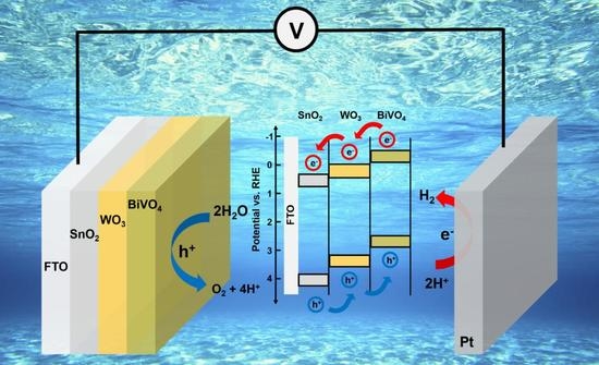
Triple Planar Heterojunction of SnO2/WO3/BiVO4 with Enhanced Photoelectrochemical Performance under Front Illumination

Department of Materials Science and Engineering, Research Institute of Advanced Materials, Seoul National University, Seoul 08826, Republic of Korea
*
Author to whom correspondence should be addressed.
Appl. Sci. 2018, 8(10), 1765; https://doi.org/10.3390/app8101765
Submission received: 31 July 2018 / Revised: 11 September 2018 / Accepted: 27 September 2018 / Published: 30 September 2018
(This article belongs to the Special Issue Nanomaterials for Solar Water Splitting)

Abstract

:
The performance of a BiVO4 photoanode is limited by poor charge transport, especially under front side illumination. Heterojunction of different metal oxides with staggered band configuration is a promising route, as it facilitates charge separation/transport and thereby improves photoactivity. We report a ternary planar heterojunction photoanode with enhanced photoactivity under front side illumination. SnO2/WO3/BiVO4 films were fabricated through electron beam deposition and subsequent wet chemical method. Remarkably high external quantum efficiency of ~80% during back side and ~90% upon front side illumination at a wavelength of 400 nm has been witnessed for SnO2/WO3/BiVO4 at 1.23 V vs. reversible hydrogen electrode (RHE). The intimate contact between the heterojunction films enabled efficient charge separation at the interface and promoted electron transport. This work provides a new paradigm for designing triple planar heterojunction to improve photoactivity, particularly under front illumination, which would be beneficial for the development of tandem devices.

Graphical Abstract

1. Introduction

Since we are heavily dependent on fossil fuels, harvesting clean energy in an efficient way is a pressing problem for mankind. Photoelectrochemical water splitting offers the capabilities to harness sunlight and convert it in the form of chemical storage through chemical bonds in the form of hydrogen [1,2,3,4].
Among various metal oxides such as Fe2O3, TiO2, WO3, and BiVO4, BiVO4 have attracted immense attention due to their promising photoelectrochemical performance, photostability, and non-toxicity [5,6,7,8,9]. BiVO4 has been recognized as a promising photocatalyst, as it possesses a relatively small band gap. However, BiVO4 suffers from low efficiency due to poor electron transport and slow water oxidation kinetics [10,11,12]. Therefore, various strategies have been adopted to overcome the limitations of BiVO4. Doping with Mo and W, and surface modifications with co-catalysts are the most common strategies adopted to improve the water oxidation efficiencies [13,14,15,16]. The main disadvantage of BiVO4 is the short electron diffusion length, ranging from 10–70 nm, which is lesser than the light absorption depth (~250 nm) [11,17,18]. The hole diffusion length of BiVO4 is around 100 nm; therefore, it is of less concern. Due to short electron diffusion length, BiVO4 exhibits high photocurrent density under backside illumination. Photogenerated electrons at the surface need to travel across a BiVO4 film during front side illumination to reach the current collector, which usually results in bulk recombination. The tandem cells have been fabricated using BiVO4 with a superior photocurrent under back illumination [19]. Performance under backside illumination is limited due to the absorption of UV photons and blue light from the transparent conducting surface. Most of the reports on BiVO4 focused on improving performance under back side illumination [20,21]. Therefore, it is necessary to fabricate BiVO4 photoanode which delivers superior pec performance during front side illumination. This would help in designing the future energy materials for the industrial scale applications.
Recently, there have been few reports of BiVO4 with heterojunction showing enhanced water oxidation performance under front illumination [22,23]. A thin film of BiVO4 was found to exhibit superior performance during front illumination [24]. BiVO4/WO3 type II heterojunctions have been intensively constructed in order to improve the light absorption capacity [25]. SnO2 thin films were found to be a hole blocking layer for BiVO4 [26]. Nanorods of SnO2 have also been used to improve the performance of BiVO4, especially under front illumination [27,28,29]. Double heterojunction of BiVO4 with SnO2 and WO3 has been fabricated to achieve an unassisted water splitting reaction [30]. However, studies on heterojunction photoanodes tuning the front illumination are rarely found in the literature.
In this work, we focus on the different thickness of double heterojunction photoanode and their influence on the performance under front illumination. We have studied SnO2/WO3/BiVO4 triple planar double heterojunction with different thicknesses and observed the change in the behavior of front illumination performance. This study would be beneficial for the construction of efficient tandem devices.

2. Experimental Section

2.1. Synthesis

Triple planar double heterojunction SnO2/WO3/BiVO4 photoanode has been fabricated through the combination of electron beam (e-beam) deposition and metal organic decomposition (MOD) technique. A SnO2 layer, followed by the deposition of a WO3 layer, has been deposited on FTO (Fluorine doped Tin Oxide) by e-beam deposition with varying thicknesses, particularly 50 nm and 100 nm at the rate of 0.3–0.4 Å/s. After depositing SnO2 on FTO, the samples were annealed at 450 °C for 1 h. WO3 has been subsequently deposited on SnO2; the samples were annealed at 500 °C for 1 h.
BiVO4 has been coated on SnO2/WO3 according to the previous report, with slight modifications [29]. The typical procedure is as follows: A drop casting solution was prepared from (0.243 g) Bi(NO3)3·5H2O and (0.123 g) VO(C5H7O2)2, which were dissolved in acetic acid and acetyl acetone. The dark green solution was stirred for 1 h to get a transparent solution. Two drops of the 5 μL were drop casted on the SnO2/WO3 and followed by heating in air at 350 °C on a hot plate for two minutes. The fabricated heterojunction photoanode was annealed in the furnace at 500 °C for 3 h in air.

2.2. Materials Characterization

The phase of SnO2/WO3/BiVO4 was confirmed by a Bruker D8 advance diffractometer, equipped with a Cu Kα source. The morphology of the SnO2/WO3/BiVO4 photoanodes was characterized using a field-emission SEM (SU-70, Hitachi), with an acceleration voltage of 5 kV and working distance of 8 mm by field emission SEM (SU-Hitachi).

2.3. Photoelectrochemical Characterization

Photoelectrochemical performances of SnO2/WO3/BiVO4 phototoanodes were measured with a typical three electrode configuration, using an Ivium potentiostat with Pt plate as a counter electrode and Ag/AgCl as a reference electrode. A 0.5 M Na2SO3 with potassium phosphate buffer solution was used as the electrolyte for all the measurements. The light intensity of a solar simulator with an AM 1.5 G filter was calibrated to 1 sun (100 mW/cm2), using a reference cell. Linear sweep voltammetry (LSV) measurements were carried out by sweeping in the anodic direction with a scan rate of 20 mV/S. The incident photon to current conversion efficiency (IPCE) values were measured at 1.23 V vs. Reversible hydrogen electrode (RHE) using light source with monochromator. Electron impedance spectroscopic (EIS) measurement was conducted at 1.23 V vs. RHE with a frequency range of 10 mHz–1000 Hz in aqueous 0.5 M Na2SO3 with phosphate buffer.

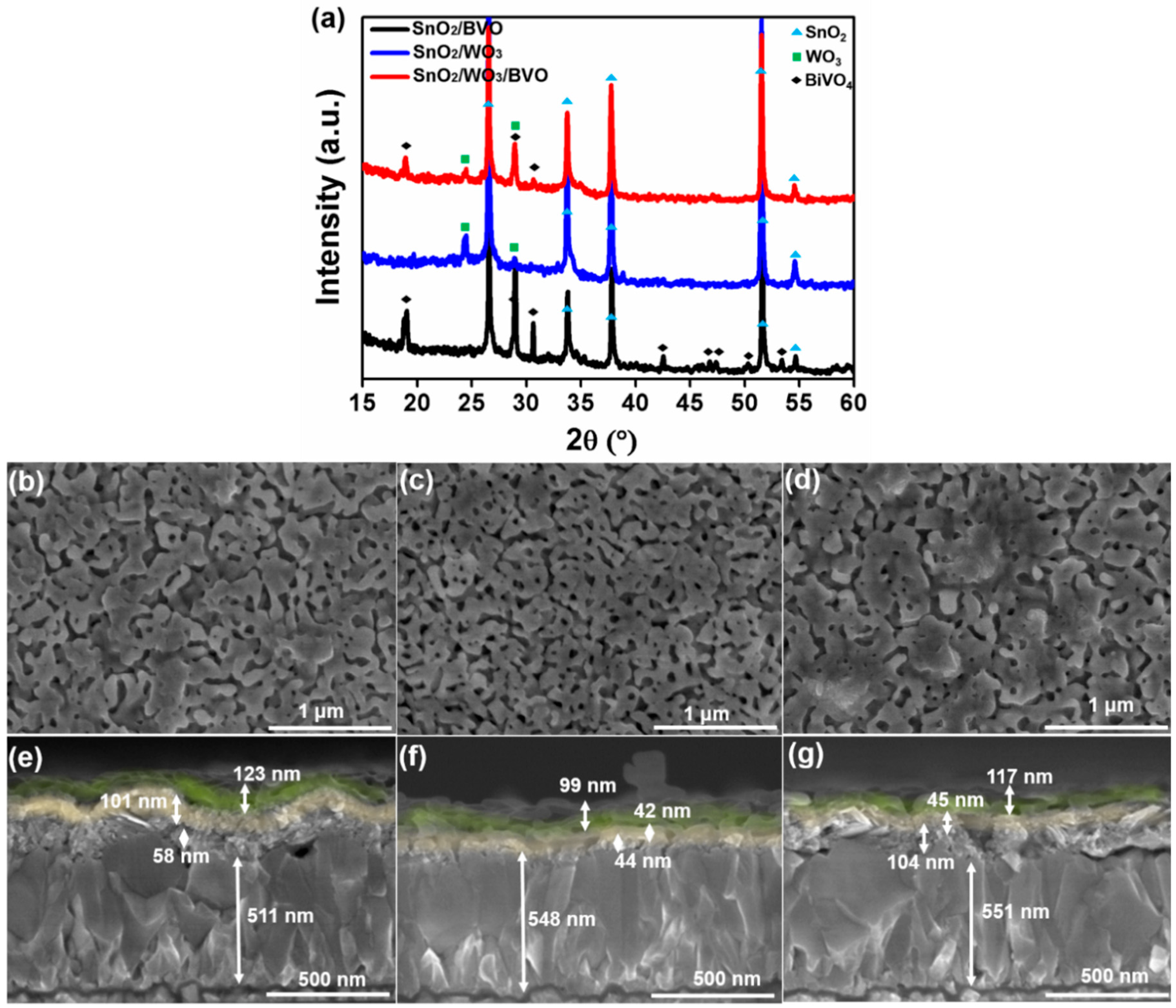
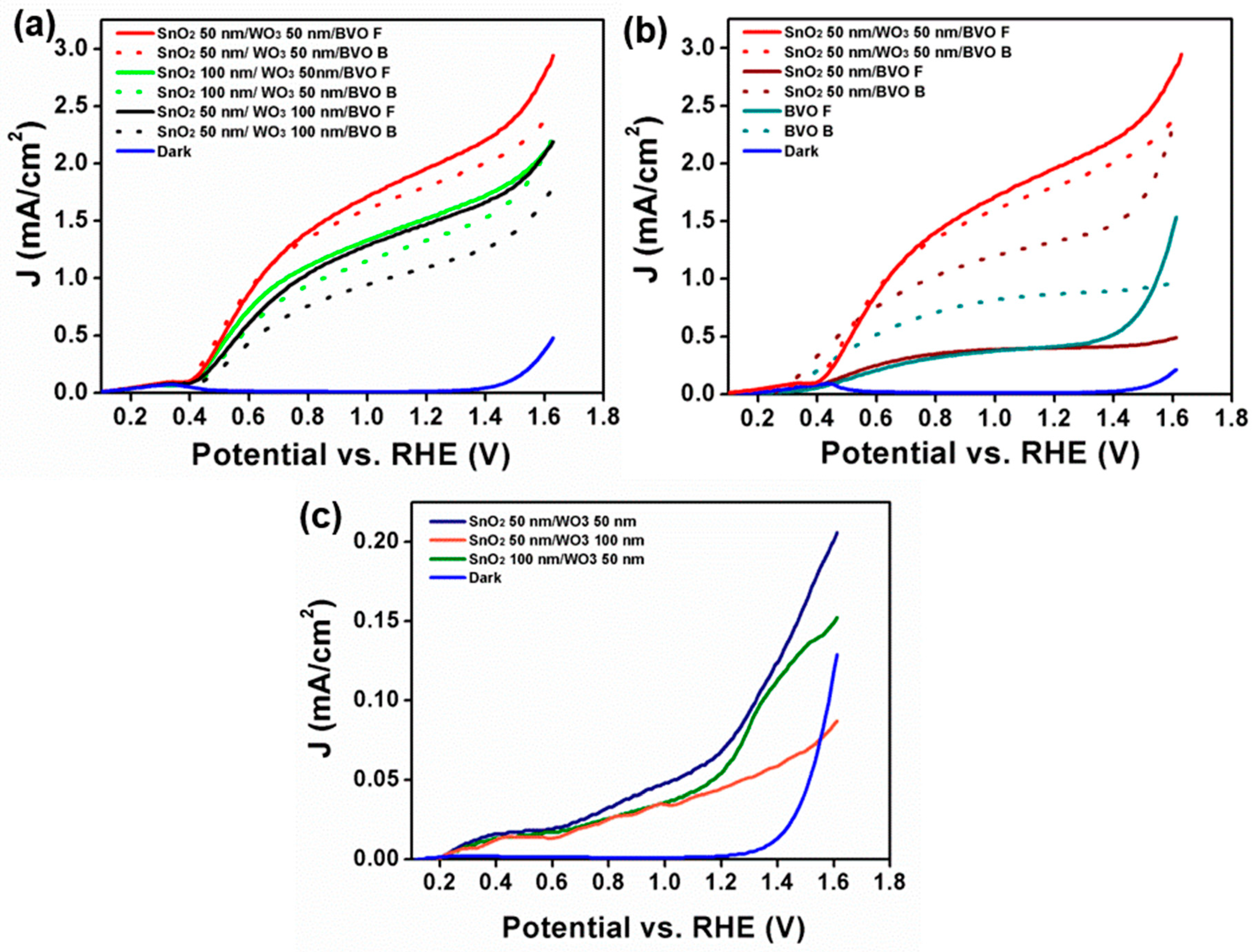
3. Results and Discussion

SnO2/WO3/BiVO4 photoanode was fabricated through the combination of e-beam deposition and MOD method. First, SnO2 was deposited on FTO with 50 and 100 nm thickness. The obtained samples were annealed at 450 °C for 1 h. WO3 was deposited on SnO2/FTO using the same technique, followed by annealing at 500 °C for 1 h. BiVO4 was coated on SnO2/WO3 using the well-known MOD technique. X-ray diffraction patterns shown in Figure 1a confirm the formation of pure phases of SnO2, WO3, and BiVO4. SEM images in Figure 1b–g reveal the morphology of triple planar heterojunction photoanode. As is clearly evident from the SEM images, the triple layers are intact with each other. There was no obvious change in the morphology of SnO2/WO3/BiVO4 after inserting the WO3 layer.
Photoelectrochemical properties of triple planar heterojunction were evaluated in three electrode configurations, using aqueous Na2SO3 with buffer solution as electrolyte (pH 7). Figure 2a presents LSV diagrams of SnO2/WO3/BiVO4 photoanode under one sun illumination. The photocurrent obtained from front and back illumination behavior was compared for different thicknesses of SnO2. We have noticed that the photocurrent obtained from front and back illumination varies with the thickness of the SnO2 and WO3. Among various thicknesses of SnO2 and WO3 in SnO2/WO3/BiVO4, SnO2 50 nm/WO3 50 nm/BiVO4 triple planar heterojunction exhibits superior performance compared to SnO2 100 nm/WO3 50 nm/BiVO4, and SnO2 50 nm/WO3 100 nm/BiVO4. SnO2 50 nm/WO3 50 nm/BiVO4 shows photocurrent density of ~2.01 mA/cm2 at 1.23 V under front side illumination, while the photocurrent during back illumination is 1.80 mA/cm2. As the thickness of WO3 increases to 100 nm, photocurrent density decreases. However, SnO2 50 nm/WO3 100 nm/BiVO4 shows a high photocurrent under front illumination compared to its back illumination. It is interesting to note that the behavior of the front and back illumination is unaffected by increasing the thickness of WO3. Figure 2b presents the LSV of SnO2 50 nm/BiVO4 under directional illumination. SnO2/BiVO4 photoanode shows ~1.2 mA/cm2 at 1.23 V during backside illumination, while it shows a photocurrent density of ~0.5 mA/cm2 under front side illumination. Photoelectrochemical properties of heterojunction SnO2 50 nm/WO3 50 nm are shown in Figure 2c.
LSV of SnO2/WO3/BiVO4 photoanode has been carried out in the absence of a hole scavenger, which is shown in Supplementary Material Figure S1a. SnO2/WO3/BiVO4 shows a reasonably good photocurrent of 1.5 mA/cm2 under front illumination at 1.23 V vs. RHE. The typical transient photo response was shown in Supplementary Material Figure S1b under chopped illumination. The instantaneous photocurrent under illumination corresponds to the immediate hole arrival at the surface. It is interesting to note that the transient photocurrent spikes are suppressed in the LSV and also in the stability measurement under chopped illumination. Usually, spikes in the transient photocurrent measurements indicate surface recombination, due to the presence of the surface states or slow water oxidation kinetics. SnO2/WO3/BiVO4 photoanode shows negligible spikes and a steady photocurrent, which demonstrates that the holes accumulated at the surface readily react with the water and hence improve photocurrent density without producing transient spikes [31].
Further, charge transfer properties have been investigated by Nyquist plots. Figure 3 depicts the Nyquist plots of SnO2/WO3/BiVO4 photoanodes. EIS were measured at 1.23 V vs. RHE under 1 Sun illumination. Nyquist plots were fitted with the equivalent circuit, using Zview software; they are presented in Figure 3 and Supplementary Material S2. Parameters extracted from the Nyquist plots are listed in Supplementary Material Table S1. In the equivalent circuit, Rs represents solution resistance, and Rct can be ascribed to charge transfer resistance at the electrode/electrolyte interface. Generally, a smaller semicircle represents the higher ability of charge transfer property of the photoanode. It is clearly evident from Figure 3 and Table S1 that the charge transfer resistance for SnO2 50 nm/WO3 50 nm/BiVO4 is lesser than that of SnO2 50 nm/BiVO4 and other thicknesses of SnO2/WO3/BiVO4 photoanodes. It demonstrates that, as the SnO2/WO3 layer is introduced beneath the BiVO4 layer, the charge transfer resistance dramatically decreases compared to the pristine BiVO4. This trend is in line with pec performance. As the thickness of WO3 and SnO2 increases from 50 nm, the electrical resistance increases. It indicates that the SnO2 50 nm/WO3 50 nm/BiVO4 has high charge separation efficiency and high water oxidation kinetics.
The stability of SnO2 50 nm/WO3 50 nm/BiVO4 has been measured in the three electrode configuration and presented in Figure 4a. It shows considerably good stability for 5 h, with negligible decrease in the photocurrent. Post mortem analysis was carried out to investigate any change in the morphology of SnO2/WO3/BiVO4 photoelectrode (Figure S3) after photostability measurement. As is evident from the SEM images of SnO2/WO3/BiVO4 (Figure S3), no serious damage to the morphology of the photoelectrode was found after photostability measurement. This result aligns with the previous reports that the photoelectrode used for the sulfite oxidation shows considerable photostability, although there could be slight dissolution of V5+ from BiVO4 [32,33]. In the present case, photostability has been studied for sulfite oxidation, as sulfite ions quickly consume the holes available on the surface of BiVO4, it does not allow holes to accumulate and trigger the photoanodic corrosion of BiVO4 very easily. It is also reported that the high quality BiVO4 can show the photostability of 500 h without undergoing any major compositional and morphological changes [32]. In addition, the WO3/BiVO4 system also exhibits considerable photostability [34]. Therefore, it is quite obvious that there is no significant change in the morphology of SnO2/WO3/BiVO4 photoelectrode after 5 h of photostability measurement.
IPCE of SnO2/WO3/BiVO4 photoanode is shown in Figure 4b. Remarkably high external quantum efficiency of ~80% during back side and ~90% upon front side illumination has been witnessed for SnO2/WO3/BiVO4 at 1.23 V vs. RHE. The photocurrent obtained by integrating the IPCE spectra (1.5 mA/cm2) is found to be in consistent with that of LSV photocurrent density. This is the highest IPCE value obtained for SnO2/WO3/BiVO4 photoanode to date.
Previous report demonstrated that the photoelectrochemical property of WO3/SnO2/BiVO4 is inferior to that of SnO2/WO3/BiVO4 [30]. Therefore, we have restricted our study only to the SnO2/WO3/BiVO4 system. It is known from the literature that introducing SnO2 under the BiVO4 layer enhances pec performance [26,27,28]. The SnO2 layer enhances the charge transfer properties of BiVO4 by suppressing the possible recombination that can occur at the interface of SnO2/BiVO4. When the WO3 layer is introduced between SnO2/BiVO4, the charge separation can be further enhanced, as seen from Figure 2a, where the photocurrent increased after the insertion of WO3 layer. It is evident from the published results that the heterojunction of nanostructured WO3/BiVO4 performs better than either of the individual materials due to the formation of type II heterojunction [35,36]. Since the band positions of both materials are suitable to construct type II heterojunction, significant separation of the photogenerated electron hole pairs can be achieved to enhance pec performance. The photogenerated electrons are transferred from BiVO4 to WO3, which has excellent electron transport property compared to BiVO4. While WO3 improves the electron transport properties, BiVO4 enhances the overall optical property of WO3 in heterojunction of SnO2/WO3/BiVO4. It is also proved in the literature that the lifetime of the photogenerated holes increases in the heterojunction compared to the individual material [37]. However, the photoelectrochemical enhancement in WO3/BiVO4 is limited by the efficient transfer of the electrons from WO3 to BiVO4. From this point of view, the double heterojunctions of SnO2/WO3/BiVO4 would certainly enhance pec performance, as can be seen from the LSV curves of SnO2/WO3/BiVO4. The schematic diagram depicting the mechanism of water splitting is demonstrated in Figure 5.
Band alignments of double heterojunction SnO2/BiVO4 also improves separation efficiency due to the lower laying valence band position [27,38,39]. Charge carrier transport has been depicted in Figure 5 for SnO2/WO3/BiVO4, which has been constructed according to the previous report [30]. The band positions have been adopted from the recent works on SnO2/WO3/BiVO4, which were determined by ultraviolent photoelectron spectroscopy and optical band gap [30,40,41]. The described band position and electron transfer in type II heterojunction, as shown in Figure 5, match well with the reported literature [36,42]. All the three layers form staggered band alignment and thereby achieve type II heterojunction, facilitating the efficient charge transport across the interface. The improved pec performance of this double heterojunction proves that there is an intimate contact between the two layers.
Unlike the previous report on SnO2/WO3/BiVO4 heterojunction, this work sheds light on photocurrent behavior under directional illumination [30]. It can clearly be seen that the performance under front and back illumination has improved after the fabrication of SnO2/WO3/BiVO4 double heterojunction. It is known that the directional dependent photoelectrochemical properties are governed by the electron transport efficiency of the materials, along with the morphology of the nanostructure [22]. In the present study, all three layers are planar and hence the directional photoelectrochemical property could be decided by both the electron transport property and the thickness of the heterojunction. The photoelectrochemical performance under front side illumination can easily be realized if the thickness is less than 100 nm, which is very close to the hole diffusion length. In the case of SnO2/WO3/BiVO4, introducing SnO2 is advantageous, as it forms cascade alignment of the band positions. The electron-hole transport also improves as the SnO2 layer acts as a hole mirror. The middle layer WO3 in SnO2/WO3/BiVO4 helps effectively in charge transport, which results in improved photoactivity of BiVO4. It is observed from SnO2/BiVO4 heterojunction that the performance under back illumination enhances, while in SnO2/WO3/BiVO4 front illumination the photocurrent is increased compared to that of back illumination. This change in the performance under directional illumination could be due to the insertion of the WO3 layer. In the case of SnO2/BiVO4 heterojunction, majority carrier transportation was limited and hence the photogenerated electron at the interface can easily reach the contact without undergoing recombination under back illumination. However, when the WO3 layer is introduced between SnO2/BiVO4 heterojunction, photocurrent density behavior changes. WO3 improves charge separation efficiency, as demonstrated by previous reports [43]. Adding SnO2/WO3 beneath the BiVO4 effectively reduces carrier recombination. Performance under front illumination is enhanced in SnO2/WO3/BiVO4, as the hole blocking layer prevents recombination. Therefore, photogenerated holes at the surface are effectively extracted to electrolyte for water oxidation while it facilitates electron diffusion to the back contact without being vulnerable to recombination. Therefore, the front illumination photocurrent has been enhanced in SnO2/WO3/BiVO4.

4. Conclusions

SnO2/WO3/BiVO4 planar heterojunction has been fabricated through a combination of the e-beam deposition method and the MOD technique. Photocurrent behavior under back and front illumination was studied for different layers of SnO2/WO3/BiVO4 planar heterojunction. When a WO3 layer was introduced between SnO2/BiVO4, photocurrent density under front illumination increased compared to that under back illumination. This indicates that poor charge carrier transport property of BiVO4 can be successively suppressed by triple planar double heterojunction. By inserting WO3 in SnO2/BiVO4, the charge transport property was improved considerably. Remarkably high IPCE of ~80% during back side and ~90% upon front side illumination was witnessed for SnO2/WO3/BiVO4 at 1.23 V vs. RHE. This study gives insights to tuning photocurrent density under directional illumination by constructing triple planar double heterojunction.

Supplementary Materials

The following are available online at https://www.mdpi.com/2076-3417/8/10/1765/s1, Figure S1: (a) LSV of SnO2/WO3/BiVO4 measured using a three-electrode configuration in aqueous phosphate buffer (pH 7.0) with 0.5 M Na2SO4 in the absence of a hole scavenger. (b) LSV of SnO2/WO3/BiVO4 in an aqueous phosphate buffer (pH 7.0) with 0.5 M Na2SO3 under chopped illumination. (c) Stability measurements of SnO2/WO3/BiVO4 under chopped illumination in an aqueous phosphate buffer (pH 7.0) with 0.5 M Na2SO3, Figure S2: Equivalent circuit model of Nyquist plot for SnO2/WO3/BiVO4 photoanode, Figure S3: SEM images of SnO2/WO3/BiVO4 (a) before and (b) after photostability measurement, Table S1: Nyquist plot fitted results for SnO2/WO3/BiVO4 photoanode.

Author Contributions

Conceptualization, H.W.J. and S.S.M.B.; Methodology, S.S.M.B.; Software, S.S.M.B.; Validation, S.S.M.B. and H.W.J.; Formal Analysis, S.S.M.B.; Investigation, S.S.M.B.; Resources, S.AL., J.M.S. and S.-P.H.; Data Curation, S.S.M.B., S.AL.; Writing-Original Draft Preparation, S.S.M.B.; Writing-Review & Editing, S.S.M.B.; Visualization, S.S.M.B.; Supervision, H.W.J.; Project Administration, H.W.J.; Funding Acquisition, H.W.J.

Funding

This work was financially supported by the Basic Science Research Program (2017R1A2B3009135), the Future Material Discovery Program (2016M3D1A1027666), the Nano Material Technology Development Program (2016M3A7B4910) through the National Research Foundation of Korea, and the International Energy Joint R&D Program of the Korea Institute of Energy Technology Evaluation and Planning (20168510011350).

Conflicts of Interest

The authors declare no conflict of interest.

References

  1. Yamamoto, M.; Tanaka, K. Artificial Molecular Photosynthetic Systems: Towards Efficient Photoelectrochemical Water Oxidation. ChemPlusChem 2016, 81, 1028–1044. [Google Scholar] [CrossRef]
  2. Xing, J.; Fang, W.Q.; Zhao, H.J.; Yang, H.G. Inorganic photocatalysts for overall water splitting. Chem. Asian J. 2012, 7, 642–657. [Google Scholar] [CrossRef] [PubMed]
  3. Takanabe, K.; Domen, K. Preparation of Inorganic Photocatalytic Materials for Overall Water Splitting. ChemCatChem 2012, 4, 1485–1497. [Google Scholar] [CrossRef]
  4. Chen, Z.; Dinh, H.N.; Miller, E. Photoelectrochemical Water Splitting Standards, Experimental Methods and Protocols; Springer: Berlin, Germany, 2013. [Google Scholar]
  5. Tamirat, A.G.; Rick, J.; Dubale, A.A.; Su, W.-N.; Hwang, B.-J. Using hematite for photoelectrochemical water splitting: A review of current progress and challenges. Nanoscale Horiz. 2016, 1, 243–267. [Google Scholar] [CrossRef]
  6. Moniz, S.J.A.; Shevlin, S.A.; Martin, D.J.; Guo, Z.-X.; Tang, J. Visible-light driven heterojunction photocatalysts for water splitting-a critical review. Energy Environ. Sci. 2015, 8, 731–759. [Google Scholar] [CrossRef]
  7. Sivula, K.; van de Krol, R. Semiconducting materials for photoelectrochemical energy conversion. Nat. Rev. Mater. 2016, 15010. [Google Scholar] [CrossRef]
  8. Bhat, S.S.M.; Jang, H.W. Recent Advances in Bismuth-Based Nanomaterials for Photoelectrochemical Water Splitting. ChemSusChem 2017, 10, 3001–3018. [Google Scholar] [CrossRef] [PubMed]
  9. Kim, D.H.; Andoshe, D.M.; Shim, Y.S.; Moon, C.W.; Sohn, W.; Choi, S.; Kim, T.L.; Lee, M.; Park, H.; Hong, K.; et al. Toward High-Performance Hematite Nanotube Photoanodes: Charge-Transfer Engineering at Heterointerfaces. ACS Appl. Mater. Interfaces 2016, 8, 23793–23800. [Google Scholar] [CrossRef] [PubMed]
  10. Walsh, A.; Yan, Y.; Huda, M.N.; Al-Jassim, M.M.; Wei, S.-H.H. Band Edge Electronic Structure of BiVO4: Elucidating the Role of the Bi s and V d Orbitals. Chem. Mater. 2009, 21, 547–551. [Google Scholar] [CrossRef]
  11. Abdi, F.F.; Van De Krol, R. Nature and light dependence of bulk recombination in Co-Pi-catalyzed BiVO4 photoanodes. J. Phys. Chem. C 2012, 116, 9398–9404. [Google Scholar] [CrossRef]
  12. Abdi, F.F.; Savenije, T.J.; May, M.M.; Dam, B.; Van De Krol, R. The origin of slow carrier transport in BiVO4 thin film photoanodes: A time-resolved microwave conductivity study. J. Phys. Chem. Lett. 2013, 4, 2752–2757. [Google Scholar] [CrossRef]
  13. Seabold, J.A.; Zhu, K.; Neale, N.R. Efficient solar photoelectrolysis by nanoporous Mo: BiVO4 through controlled electron transport. Phys. Chem. Chem. Phys. 2014, 16, 1121–1131. [Google Scholar] [CrossRef] [PubMed]
  14. Jeong, H.W.; Jeon, T.H.; Jang, J.S.; Choi, W.; Park, H. Strategic modification of BiVO4 for improving photoelectrochemical water oxidation performance. J. Phys. Chem. C 2013, 117, 9104–9112. [Google Scholar] [CrossRef]
  15. Shi, X.; Choi, I.Y.; Zhang, K.; Kwon, J.; Kim, D.Y.; Lee, J.K.; Oh, S.H.; Kim, J.K.; Park, J.H. Efficient photoelectrochemical hydrogen production from bismuth vanadate-decorated tungsten trioxide helix nanostructures. Nat. Commun. 2014, 5, 1–8. [Google Scholar] [CrossRef] [PubMed]
  16. Zhong, D.K.; Choi, S.; Gamelin, D.R. Near-complete suppression of surface recombination in solar photoelectrolysis by “Co-Pi” catalyst-modified W: BiVO4. J. Am. Chem. Soc. 2011, 133, 18370–18377. [Google Scholar] [CrossRef] [PubMed]
  17. Butler, K.T.; Dringoli, B.J.; Zhou, L.; Rao, P.M.; Walsh, A.; Titova, L.V. Ultrafast carrier dynamics in BiVO4 thin film photoanode material: Interplay between free carriers, trapped carriers and low-frequency lattice vibrations. J. Mater. Chem. A 2016, 4, 18516–18523. [Google Scholar] [CrossRef]
  18. Liu, T.; Pasumarthi, V.; Laporte, C.; Feng, Z.; Li, Q.; Yang, J.; Li, C.; Dupuis, M. Bimodal hole transport in bulk BiVO4 from computation. J. Mater. Chem. A 2018, 6, 3714–3723. [Google Scholar] [CrossRef]
  19. Bornoz, P.; Abdi, F.F.; Tilley, S.D.; Dam, B.; Van De Krol, R.; Graetzel, M.; Sivula, K. A bismuth vanadate-cuprous oxide tandem cell for overall solar water splitting. J. Phys. Chem. C 2014, 118, 16959–16966. [Google Scholar] [CrossRef]
  20. Zhang, Y.; Wang, D.; Zhang, X.; Chen, Y.; Kong, L.; Chen, P.; Wang, Y.; Wang, C.; Wang, L.; Liu, Y. Enhanced photoelectrochemical performance of nanoporous BiVO4 photoanode by combining surface deposited cobalt-phosphate with hydrogenation treatment. Electrochim. Acta 2016, 195, 51–58. [Google Scholar] [CrossRef]
  21. Chae, S.Y.; Lee, C.S.; Jung, H.; Joo, O.-S.; Min, B.K.; Kim, J.H.; Hwang, Y.J. Insight into Charge Separation in WO3/BiVO4 Heterojunction for Solar Water Splitting. ACS Appl. Mater. Interfaces 2017, 9, 19780–19790. [Google Scholar] [CrossRef] [PubMed]
  22. Kuang, Y.; Jia, Q.; Nishiyama, H.; Yamada, T.; Kudo, A.; Domen, K. A front-illuminated nanostructured transparent BiVO4 photoanode for >2% efficient water splitting. Adv. Energy Mater. 2016, 6, 2–8. [Google Scholar] [CrossRef]
  23. Chen, L.; Alarcon-Llado, E.; Hettick, M.; Sharp, I.D.; Lin, Y.; Javey, A.; Ager, J.W. Reactive sputtering of bismuth vanadate photoanodes for solar Water splitting. J. Phys. Chem. C 2013, 117, 21635–21642. [Google Scholar] [CrossRef]
  24. Liang, Y.; Tsubota, T.; Mooij, L.P.A.; Van De Krol, R. Highly improved quantum efficiencies for thin film BiVO4 photoanodes. J. Phys. Chem. C 2011, 115, 17594–17598. [Google Scholar] [CrossRef]
  25. Chae, S.Y.; Jung, H.; Jeon, H.S.; Min, B.K.; Hwang, Y.J.; Joo, O.-S. Morphology control of one-dimensional heterojunctions for highly efficient photoanodes used for solar water splitting. J. Mater. Chem. A 2014, 2, 11408. [Google Scholar] [CrossRef]
  26. Byun, S.; Kim, B.; Jeon, S.; Shin, B. Effects of a SnO2 hole blocking layer in a BiVO4-based photoanode on photoelectrocatalytic water oxidation. J. Mater. Chem. A 2017, 5, 6905–6913. [Google Scholar] [CrossRef]
  27. Zhou, L.; Yang, Y.; Zhang, J.; Rao, P.M. Photoanode with Enhanced Performance Achieved by Coating BiVO4 onto ZnO-Templated Sb-Doped SnO2 Nanotube Scaffold. ACS Appl. Mater. Interfaces 2017, 9, 11356–11362. [Google Scholar] [CrossRef] [PubMed]
  28. Zhou, L.; Zhao, C.; Giri, B.; Allen, P.; Xu, X.; Joshi, H.; Fan, Y.; Titova, L.V.; Rao, P.M. High Light Absorption and Charge Separation Efficiency at Low Applied Voltage from Sb-Doped SnO2/BiVO4 Core/Shell Nanorod-Array Photoanodes. Nano Lett. 2016, 16, 3463–3474. [Google Scholar] [CrossRef] [PubMed]
  29. Bhat, S.S.M.; Suh, J.M.; Choi, S.; Hong, S.-P.; Lee, S.A.; Kim, C.; Moon, C.W.; Lee, M.G.; Jang, H.W. Substantially enhanced front illumination photocurrent in porous SnO2 nanorods/networked BiVO4 heterojunction photoanodes. J. Mater. Chem. A 2018. [Google Scholar] [CrossRef]
  30. Baek, J.H.; Kim, B.J.; Han, G.S.; Hwang, S.W.; Kim, D.R.; Cho, I.S.; Jung, H.S. BiVO4/WO3/SnO2 double-heterojunction photoanode with enhanced charge separation and visible-transparency for bias-free solar water-splitting with a perovskite solar cell. ACS Appl. Mater. Interfaces 2017, 9, 1479–1487. [Google Scholar] [CrossRef] [PubMed]
  31. Kamimura, J.; Bogdanoff, P.; Abdi, F.F.; Lähnemann, J.; Van De Krol, R.; Riechert, H.; Geelhaar, L. Photoelectrochemical Properties of GaN Photoanodes with Cobalt Phosphate Catalyst for Solar Water Splitting in Neutral Electrolyte. J. Phys. Chem. C 2017, 121, 12540–12545. [Google Scholar] [CrossRef]
  32. Lee, D.K.; Choi, K.-S. Enhancing long-term photostability of BiVO4 photoanodes for solar water splitting by tuning electrolyte composition. Nat. Energy 2017, 3, 53–60. [Google Scholar] [CrossRef]
  33. Grigioni, I.; Corti, A.; Dozzi, M.V.; Selli, E. Photoactivity and Stability of WO3/BiVO4 Photoanodes: Effects of the Contact Electrolyte and of Ni/Fe Oxyhydroxide Protection. J. Phys. Chem. C 2018, 122, 13969–13978. [Google Scholar] [CrossRef]
  34. Kalanur, S.S.; Yoo, I.H.; Park, J.; Seo, H. Insights into the electronic bands of WO3/BiVO4/TiO2, revealing high solar water splitting efficiency. J. Mater. Chem. A 2017, 5, 1455–1461. [Google Scholar] [CrossRef]
  35. Grigioni, I.; Stamplecoskie, K.G.; Selli, E.; Kamat, P.V. Dynamics of Photogenerated Charge Carriers in WO3/BiVO4 Heterojunction Photoanodes. J. Phys. Chem. C 2015, 119, 20792–20800. [Google Scholar] [CrossRef]
  36. Rao, P.M.; Cai, L.; Liu, C.; Cho, I.S.; Lee, C.H.; Weisse, J.M.; Yang, P.; Zheng, X. Simultaneously efficient light absorption and charge separation in WO3/BiVO4 Core/shell nanowire photoanode for photoelectrochemical water oxidation. Nano Lett. 2014, 14, 1099–1105. [Google Scholar] [CrossRef] [PubMed]
  37. Zhou, Y.; Zhang, L.; Lin, L.; Wygant, B.R.; Liu, Y.; Zhu, Y.; Zheng, Y.; Mullins, C.B.; Zhao, Y.; Zhang, X.; et al. Highly Efficient Photoelectrochemical Water Splitting from Hierarchical WO3/BiVO4 Nanoporous Sphere Arrays. Nano Lett. 2017, 17, 8012–8017. [Google Scholar] [CrossRef] [PubMed]
  38. Zhou, S.; Tang, R.; Zhang, L.; Yin, L. Au Nanoparticles coupled Three-dimensional Macroporous BiVO4/SnO2 Inverse Opal Heterostructure for Efficient Photoelectrochemical Water Splitting. Electrochim. Acta 2017, 248, 593–602. [Google Scholar] [CrossRef]
  39. Chen, S.; Yang, J.; Wu, J. Three-Dimensional Undoped Crystalline SnO2 Nanodendrite Arrays Enable Efficient Charge Separation in BiVO4/SnO2 Heterojunction Photoanodes for Photoelectrochemical Water Splitting. ACS Appl. Energy Mater. 2018, 1, 2143–2149. [Google Scholar] [CrossRef]
  40. Resasco, J.; Zhang, H.; Kornienko, N.; Becknell, N.; Lee, H.; Guo, J.; Briseno, A.L.; Yang, P. TiO2/BiVO4 Nanowire Heterostructure Photoanodes Based on Type II Band Alignment. ACS Cent. Sci. 2016, 2, 80–88. [Google Scholar] [CrossRef] [PubMed]
  41. Hong, S.J.; Lee, S.; Jang, J.S.; Lee, J.S. Heterojunction BiVO4/WO3 electrodes for enhanced photoactivity of water oxidation. Energy Environ. Sci. 2011, 4, 1781. [Google Scholar] [CrossRef]
  42. Chatchai, P.; Murakami, Y.; Kishioka, S.; Nosaka, A.Y.; Nosaka, Y. Efficient photocatalytic activity of water oxidation over WO3/BiVO4 composite under visible light irradiation. Electrochim. Acta 2009, 54, 1147–1152. [Google Scholar] [CrossRef]
  43. Shi, X.; Herraiz-Cardona, I.; Bertoluzzi, L.; Lopez-Varo, P.; Bisquert, J.; Park, J.H.; Gimenez, S. Understanding the synergistic effect of WO3–BiVO4 heterostructures by impedance spectroscopy. Phys. Chem. Chem. Phys. 2016, 18, 9255–9261. [Google Scholar] [CrossRef] [PubMed]
Figure 1. (a) XRD patterns of SnO2/WO3/BiVO4. Scanning electron microscopic (SEM) top images of (b) SnO2 50 nm/WO3 100 nm/BiVO4 (c) SnO2 50 nm/WO3 50 nm/BiVO4 (d) SnO2 100 nm/WO3 50 nm/BiVO4. SEM cross-section images of (e) SnO2 50 nm/WO3 100 nm/BiVO4 on FTO substrate (f) SnO2 50 nm/WO3 50 nm/BiVO4 (g) SnO2 100 nm/WO3 50 nm/BiVO4.
Applsci 08 01765 g001
Figure 2. (a) LSV of SnO2/WO3/BiVO4 under front (F) and back (B) illumination; (b) Photocurrent density under back and front illumination for SnO2/BiVO4 in comparison with SnO2/WO3/BiVO4; (c) LSV of SnO2/WO3 photoanode measured using a three-electrode configuration set up in aqueous phosphate buffer (pH 7.0) with 0.5 M Na2SO3.
Applsci 08 01765 g002
Figure 3. (a) Electron impedance spectra (EIS) of SnO2/WO3/BiVO4; (b) Zoomed region of EIS spectra of (a) for SnO2/WO3/BiVO4 photoanode, measured using a three-electrode configuration set up in an aqueous phosphate buffer (pH 7.0) with 0.5 M Na2SO3 at 1.23 V vs. Reversible hydrogen electrode (RHE).
Applsci 08 01765 g003
Figure 4. (a) Stability measurement for SnO2/WO3/BiVO4; (b) Incident photon to current conversion efficiency (IPCE) of SnO2/WO3/BiVO4 photoanode measured using a three-electrode configuration set up in an aqueous phosphate buffer (pH 7.0) with 0.5 M Na2SO3 at 1.23 V vs. RHE.
Applsci 08 01765 g004
Figure 5. Schematic diagram for SnO2/WO3/BiVO4, depicting the mechanism of water splitting.
Applsci 08 01765 g005

