Sub-Wavelength Scale Si Inverted Pyramid Fabrication with Enhanced Size Control by Using Silica Sphere Lithography Technique


Abstract
1. Introduction
2. Experimental
3. Results and Discussion
3.1. Deposition of Silica Sphere Monolayer
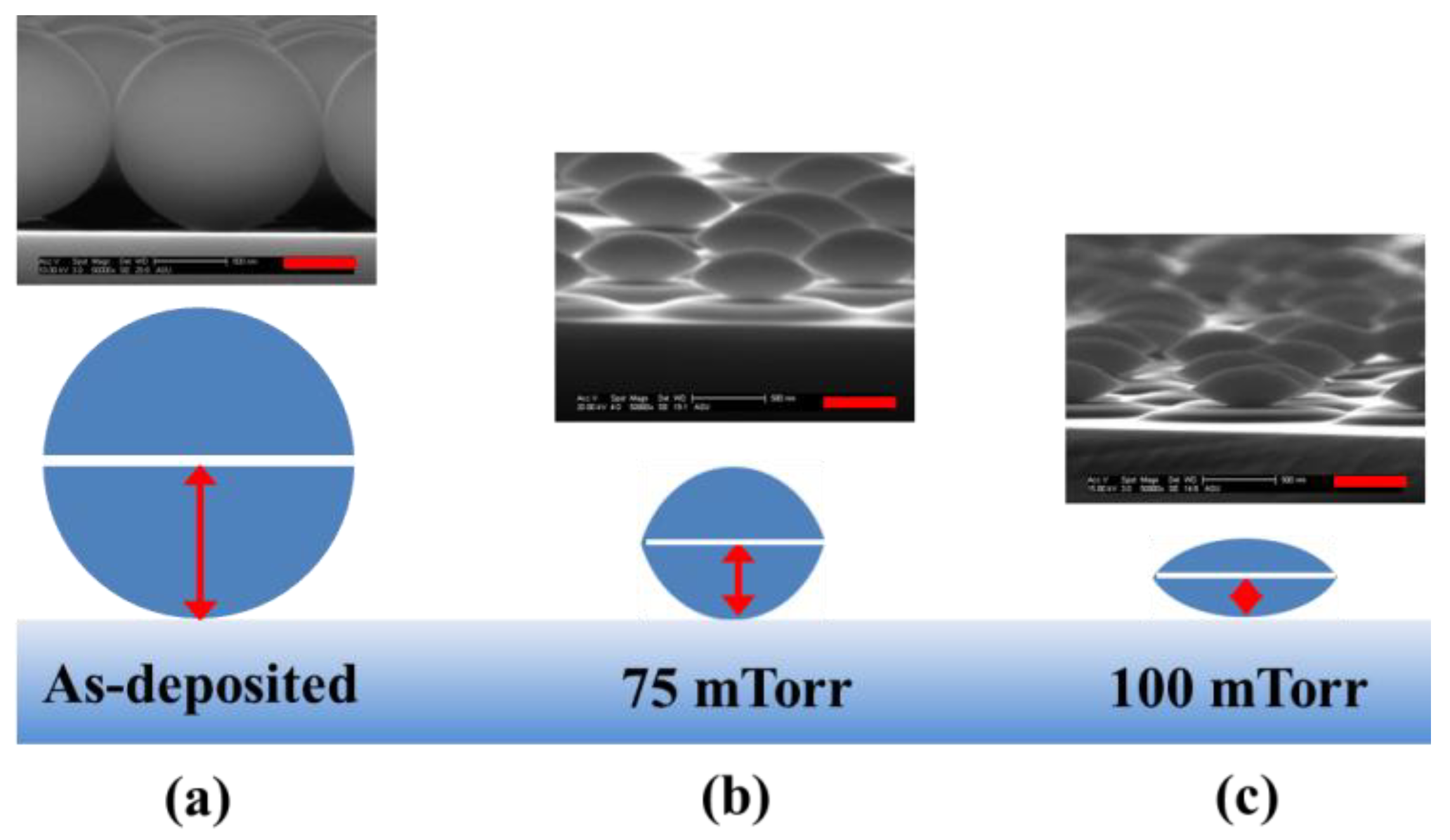
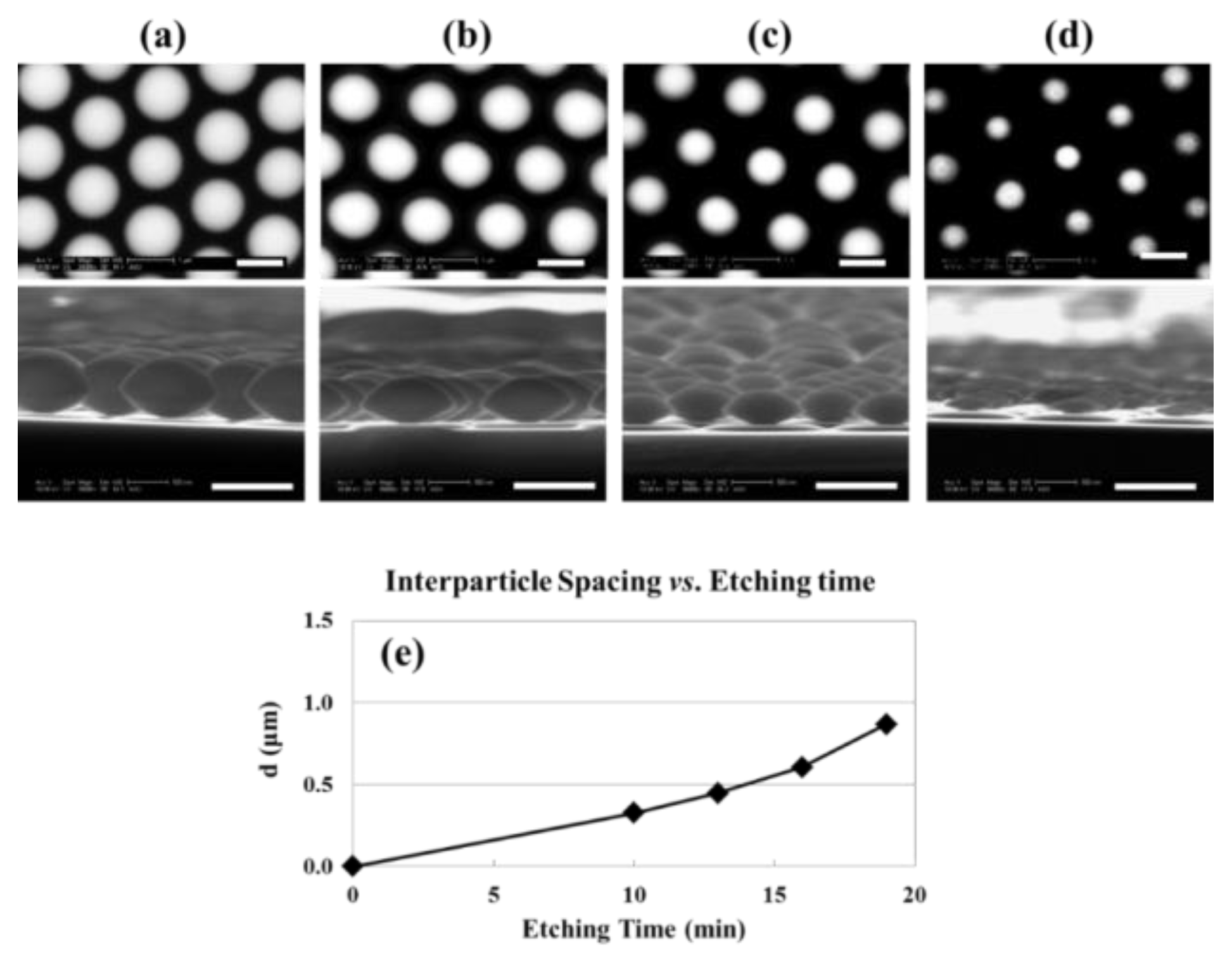
3.2. Silica Sphere Size Control by RIE
3.3. Mask Layer Deposition and SS Removal
3.4. SWSS Fabrication: Inverted Pyramid
4. Conclusions
Author Contributions
Funding
Conflicts of Interest
References
- Herasimenka, S.Y.; Dauksher, W.J.; Bowden, S.G. >750 mV open circuit voltage measured on 50 μm thick silicon heterojunction solar cell. Appl. Phys. Lett. 2013, 103, 053511. [Google Scholar] [CrossRef]
- Taguchi, M.; Yano, A.; Tohoda, S.; Matsuyama, K.; Nakamura, Y.; Nishiwaki, T.; Fujita, K.; Maruyama, E. 24.7% Record Efficiency HIT Solar Cell on Thin Silicon Wafer. IEEE J. Photovolt. 2014, 44, 96–99. [Google Scholar] [CrossRef]
- Tian, B.; Zheng, X.; Kempa, T.J.; Fang, Y.; Yu, N.; Yu, G.; Huang, J.; Lieber, C.M. Coaxial silicon nanowires as solar cells and nanoelectronic power sources. Nature 2007, 449, 885–889. [Google Scholar] [CrossRef] [PubMed]
- Chutinan, A.; John, S. Light trapping and absorption optimization in certain thin-film photonic crystal architectures. Phys. Rev. A 2008, 78, 023825. [Google Scholar] [CrossRef]
- Tobias, I.; Luque, A.; Marti, A. Light intensity enhancement by diffracting structures in solar cells. J. Appl. Phys. 2008, 104, 034502. [Google Scholar] [CrossRef]
- Lin, C.; Povinelli, M.L. Optical absorption enhancement in silicon nanowire arrays with a large lattice constant for photovoltaic applications. Opt. Express 2009, 17, 19371–19381. [Google Scholar] [CrossRef] [PubMed]
- Mavrokefalos, A.; Han, S.E.; Yerci, S.; Branham, M.S.; Chen, G. Efficient Light Trapping in Inverted Nanopyramid Thin Crystalline Silicon Membranes for Solar Cell Applications. Nano Lett. 2012, 12, 2792–2796. [Google Scholar] [CrossRef] [PubMed]
- Jeong, S.; McGehee, M.D.; Cui, Y. All-back-contact ultra-thin silicon nanocone solar cells with 13.7% power conversion efficiency. Nat. Commun. 2013, 4, 2950. [Google Scholar] [CrossRef] [PubMed]
- Juhasz, R.; Elfstrom, N.; Linnros, J. Controlled fabrication of silicon nanowires by electron beam lithography and electrochemical size reduction. Nano Lett. 2005, 55, 275–280. [Google Scholar] [CrossRef] [PubMed]
- Zhang, J.; Shokouhi, B.; Cui, B. Tilted nanostructure fabrication by electron beam lithography. J. Vac. Sci. Technol. B 2012, 30, 06F302. [Google Scholar] [CrossRef]
- Ertorer, E.; Vasefi, F.; Keshwah, J.; Najiminaini, M.; Halfpap, C.; Langbein, U.; Carson, J.J.L.; Hamilton, D.W.; Mittler, S. Large area periodic, systematically changing, multishape nanostructures by laser interference lithography and cell response to these topographies. J. Biomed. Opt. 2013, 18, 035002. [Google Scholar] [CrossRef] [PubMed]
- Tan, C.; Peng, C.S.; Pakarinen, J.; Pessa, M.; Petryakov, V.N.; Verevkin, Y.K.; Zhang, J.; Wang, Z.; Olaizola, S.M.; Berthou, T. Ordered nanostructures written directly by laser interference. Nanotechnology 2009, 20, 12. [Google Scholar] [CrossRef] [PubMed]
- Choi, J.Y.; Honsberg, C.B. Reactive Ion Etching Surface Texturing of c-Si using Silica Nanosphere lithography technique for Solar Cell Application. Presented at 2013 IEEE 39th Photovoltaic Specialists Conference, Tampa, FL, USA, 16–21 June 2013. [Google Scholar]
- Mihi, A.; Ocana, M.; Miguez, H. Oriented colloidal-crystal thin films by spin-coating microspheres dispersed in volatile media. Adv. Mater. 2006, 18, 2244–2249. [Google Scholar] [CrossRef]
- Huang, J.X.; Kim, F.; Tao, A.R.; Connor, S.; Yang, P. Spontaneous formation of nanoparticle stripe patterns through dewetting. Nat. Mater. 2005, 44, 896–900. [Google Scholar] [CrossRef] [PubMed]
- Hsu, C.M.; Connor, S.T.; Tang, M.X.; Cui, Y. Wafer-scale silicon nanopillars and nanocones by Langmuir-Blodgett assembly and etching. Appl. Phys. Lett. 2008, 93, 133109. [Google Scholar] [CrossRef]
- Jiang, P.; Prasad, T.; McFarland, M.J.; Colvin, V.L. Two-dimensional nonclose-packed colloidal crystals formed by spincoating. Appl. Phys. Lett. 2006, 89, 011908. [Google Scholar] [CrossRef]
- Cho, W.J.; Chin, W.K.; Kuo, C.T. Effects of alcoholic moderators on anisotropic etching of silicon in aqueous potassium hydroxide solutions. Sens. Actuators A 2004, 116, 357–368. [Google Scholar] [CrossRef]
- Zubel, I. Silicon anisotropic etching in alkaline solutions III: On the possibility of spatial structures forming in the course of Si(100) anisotropic etching in KOH and KOH plus IPA solutions. Sens. Actuators A 2000, 84, 116–125. [Google Scholar] [CrossRef]
- Rasband, W. Imagej; U.S. National Institutes of Health: Bethesda, MD, USA, 1997–2006. Available online: https://imagej.nih.gov/ij/ (accessed on 1 August 2018).
- Ogi, T.; Modesto-Lopez, L.B.; Iskandara, F.; Okuyama, K. Fabrication of a large area monolayer of silica particles on a sapphire substrate by a spin coating method. Colloids Surf. A 2007, 297, 71–78. [Google Scholar] [CrossRef]
- Rykaczewski, K.; Hildreth, O.J.; Wong, C.P.; Fedorov, A.G.; Scott, J.H.J. Guided Three-Dimensional Catalyst Folding during Metal-Assisted Chemical Etching of Silicon. Nano Lett. 2011, 11, 2369–2374. [Google Scholar] [CrossRef] [PubMed]
- Zhang, L.; Qiao, S.Z.; Jin, Y.G.; Chen, Z.G.; Gu, H.C.; Lu, G.Q. Magnetic hollow spheres of periodic mesoporous organosilica and Fe3O4 nanocrystals: Fabrication and structure control. Adv. Mater. 2008, 20, 805–809. [Google Scholar] [CrossRef]
- Izak-Nau, E.; Voetz, M.; Eiden, S.; Duschl, A.; Puntes, V.F. Altered characteristics of silica nanoparticles in bovine and human serum: The importance of nanomaterial characterization prior to its toxicological evaluation. Part. Fibre Toxicol. 2013, 10, 56. [Google Scholar] [CrossRef] [PubMed]
- Wan, Q.; Ramsey, C.; Baran, G. Thermal pretreatment of silica composite filler materials. J. Therm. Anal. Calorim. 2010, 99, 237–243. [Google Scholar] [CrossRef] [PubMed]
- Schneider, C.A.; Rasband, W.S.; Eliceiri, K.W. NIH Image to ImageJ: 25 years of image analysis. Nat. Methods 2012, 99, 671–675. [Google Scholar] [CrossRef]
- Choi, J.-Y.; Alford, T.L.; Honsberg, C.B. Solvent-Controlled Spin-Coating Method for Large-Scale Area Deposition of Two-Dimensional Silica Nanosphere Assembled Layers. Langmuir 2014, 30, 5732–5738. [Google Scholar] [CrossRef] [PubMed]
- Hulteen, J.C.; Vanduyne, R.P. Nanosphere lithography: A materials general fabrication process for periodic particle array surfaces. J. Vac. Sci. Technol. A 1995, 13, 1553–1558. [Google Scholar] [CrossRef]
- Denkov, N.; Velev, O.; Kralchevski, P.; Ivanov, I.; Yoshimura, H.; Nagayama, K. Mechanism of formation of two-dimensional crystals from latex particles on substrates. Langmuir 1992, 88, 3183–3190. [Google Scholar] [CrossRef]
- Jansen, H.; Gardeniers, H.; de Boer, M.; Elwenspoek, M.; Fluitman, J. A survey on the reactive ion etching of silicon in microtechnology. J. Micromech. Microeng. 1996, 66, 14–28. [Google Scholar] [CrossRef]
- Cheung, C.L.; Nikolić, R.J.; Reinhardt, C.E.; Wang, T.F. Fabrication of nanopillars by nanosphere lithography. Nanotechnology 2006, 17, 1339–1343. [Google Scholar] [CrossRef]
- Oh, N.R.; Song, T.J.; Lim, S.K.; Yoon, C.S. Polystyrene Nanosphere Lithography Improved by the Insertion of a Sacrificial Polyimide Film. Electron. Mater. Lett. 2005, 11, 135–139. [Google Scholar]
- Easwarakhanthana, T.; Beyssen, D.; Le Brizoual, L.; Bougdira, J. Spectroellipsometric analysis of CHF3 plasma-polymerized fluorocarbon films. J. Vac. Sci. Technol. A 2006, 24, 1036–1043. [Google Scholar] [CrossRef]


| PressureProperty | 50 mTorr | 75 mTorr | 100 mTorr |
|---|---|---|---|
| Cross-sectional SEM Image (Scale-bar:500 nm) |  |  |  |
| Vertical Etching Rate (nm/min) | 90.3 | 80.3 | 70.3 |
| Horizontal Etching Rate (nm/min) | 34.8 | 30.3 | 18.1 |
| Vertical/Horizontal Etching Ratio | 2.6 | 2.6 | 3.9 |
© 2018 by the authors. Licensee MDPI, Basel, Switzerland. This article is an open access article distributed under the terms and conditions of the Creative Commons Attribution (CC BY) license (http://creativecommons.org/licenses/by/4.0/).
Share and Cite
Choi, J.-Y.; Honsberg, C.B. Sub-Wavelength Scale Si Inverted Pyramid Fabrication with Enhanced Size Control by Using Silica Sphere Lithography Technique. Appl. Sci. 2018, 8, 1720. https://doi.org/10.3390/app8101720
Choi J-Y, Honsberg CB. Sub-Wavelength Scale Si Inverted Pyramid Fabrication with Enhanced Size Control by Using Silica Sphere Lithography Technique. Applied Sciences. 2018; 8(10):1720. https://doi.org/10.3390/app8101720
Chicago/Turabian StyleChoi, Jea-Young, and Christiana B. Honsberg. 2018. "Sub-Wavelength Scale Si Inverted Pyramid Fabrication with Enhanced Size Control by Using Silica Sphere Lithography Technique" Applied Sciences 8, no. 10: 1720. https://doi.org/10.3390/app8101720
APA StyleChoi, J.-Y., & Honsberg, C. B. (2018). Sub-Wavelength Scale Si Inverted Pyramid Fabrication with Enhanced Size Control by Using Silica Sphere Lithography Technique. Applied Sciences, 8(10), 1720. https://doi.org/10.3390/app8101720