DNA as Functional Material in Organic-Based Electronics


Abstract
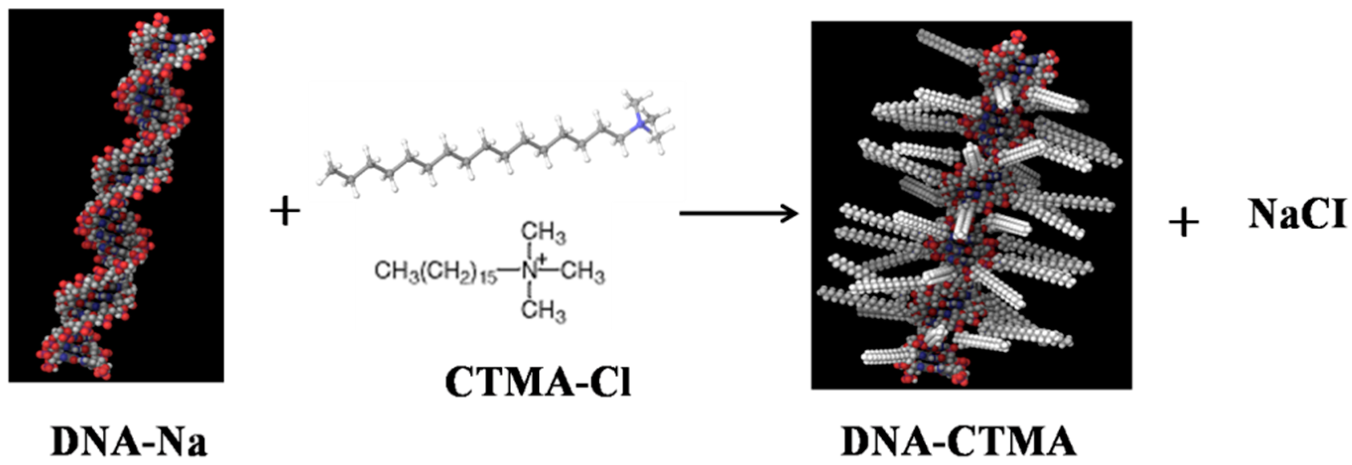
:1. Introduction
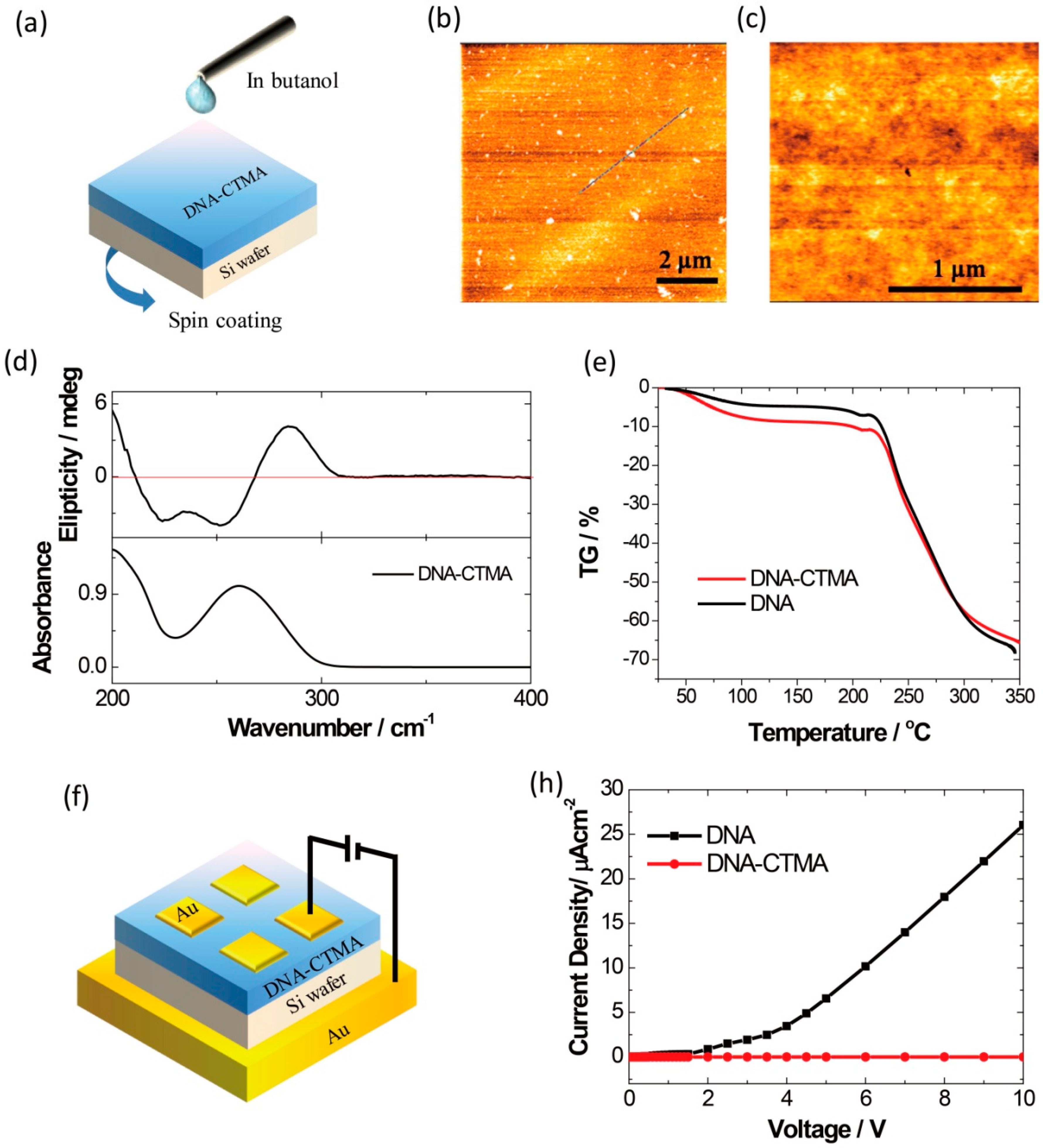
2. Physical Performance of DNA Thin Film
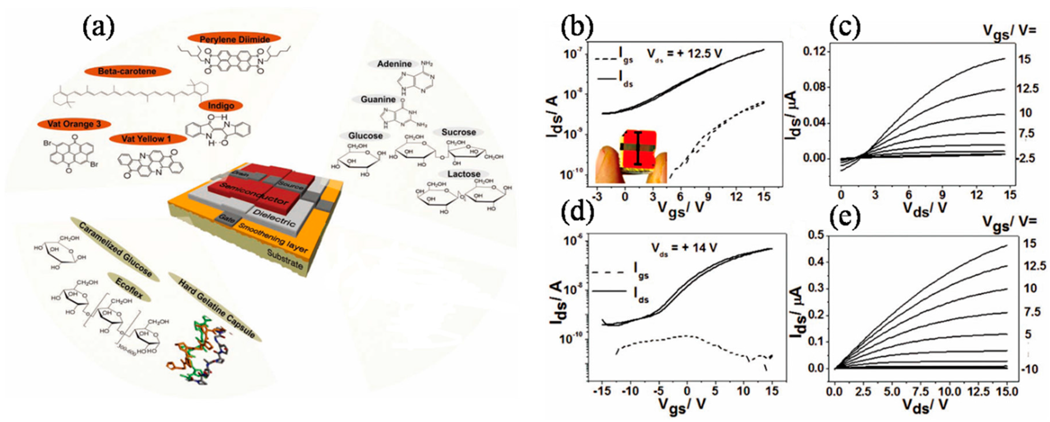
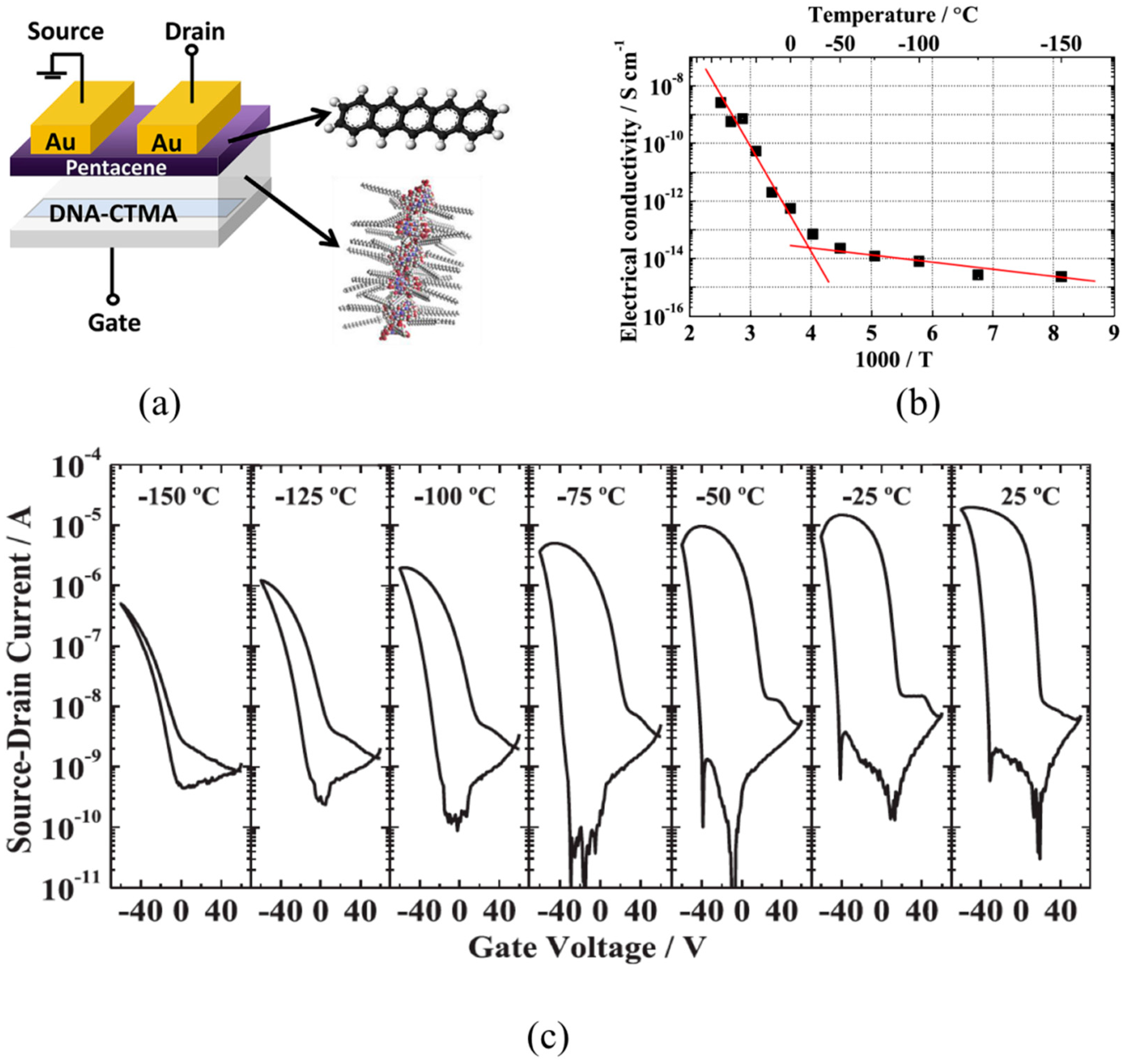
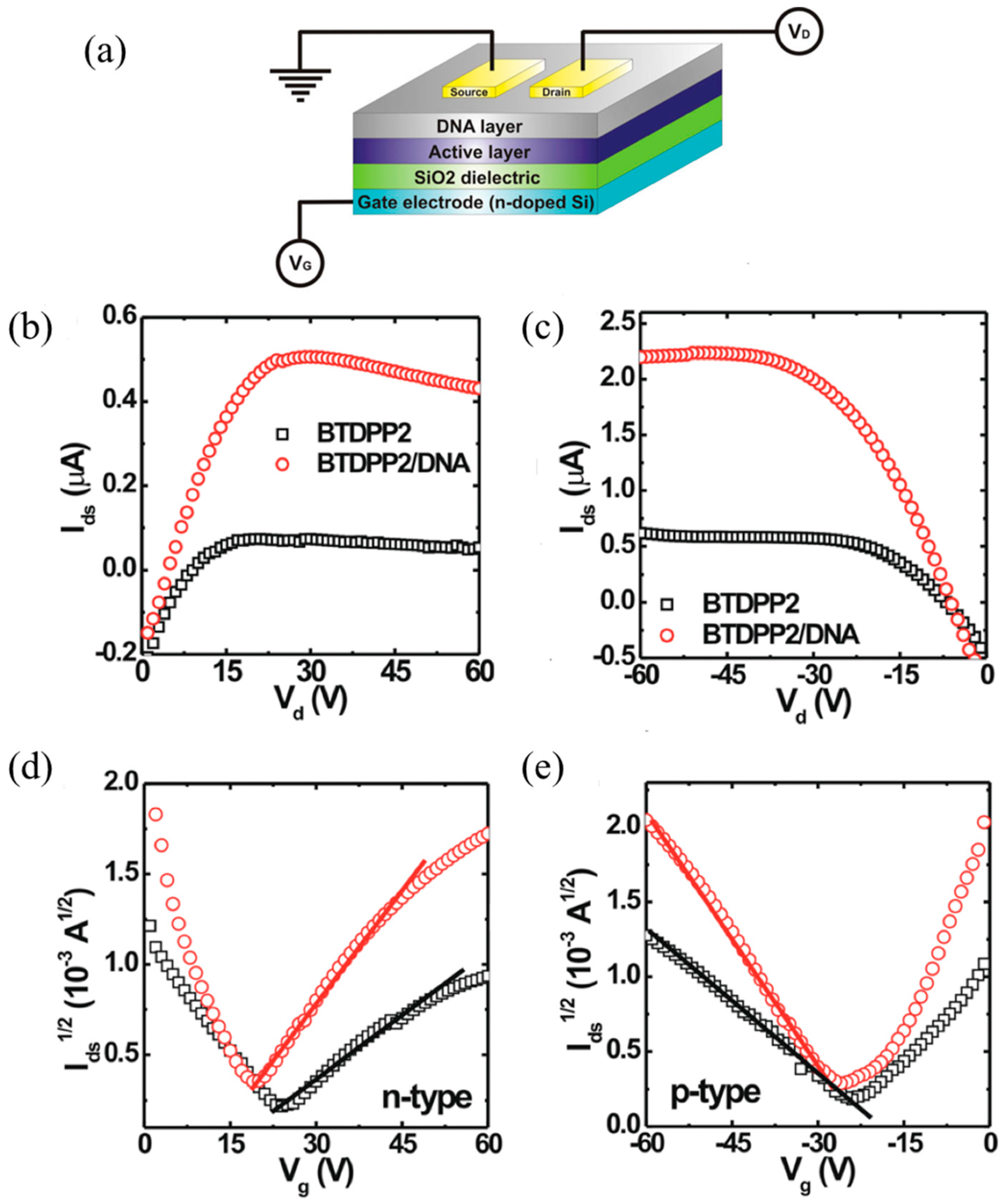
3. DNA as Functional Layers for OTFTs
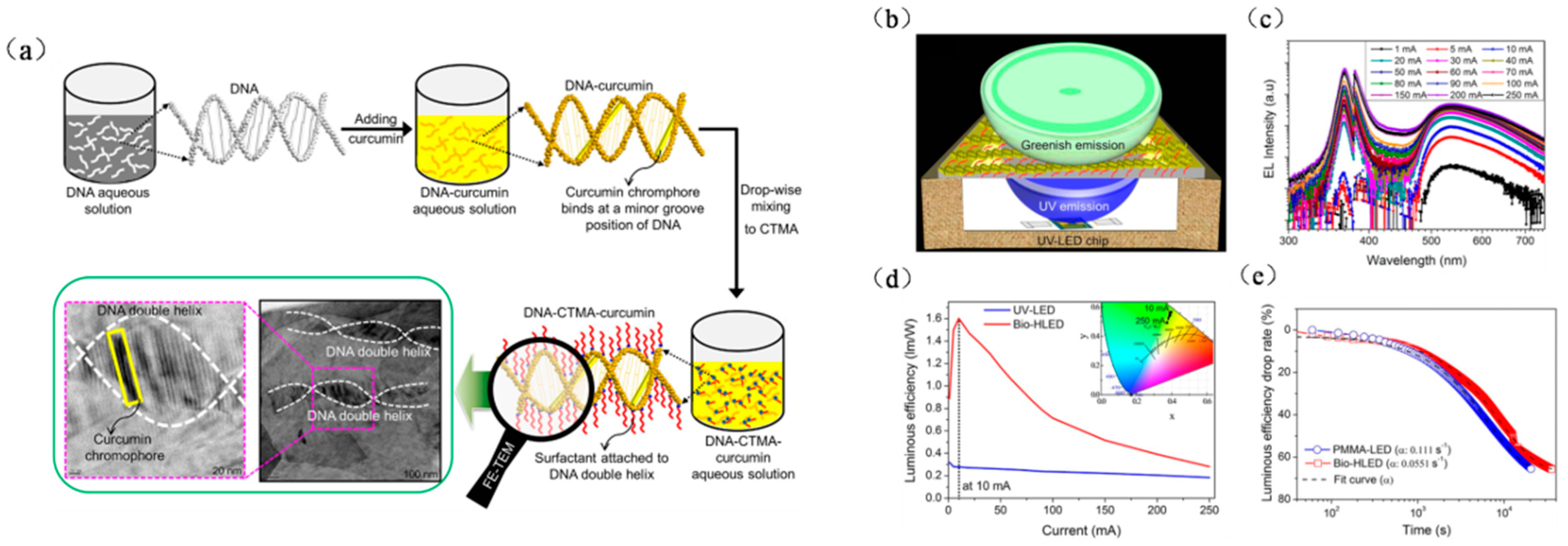
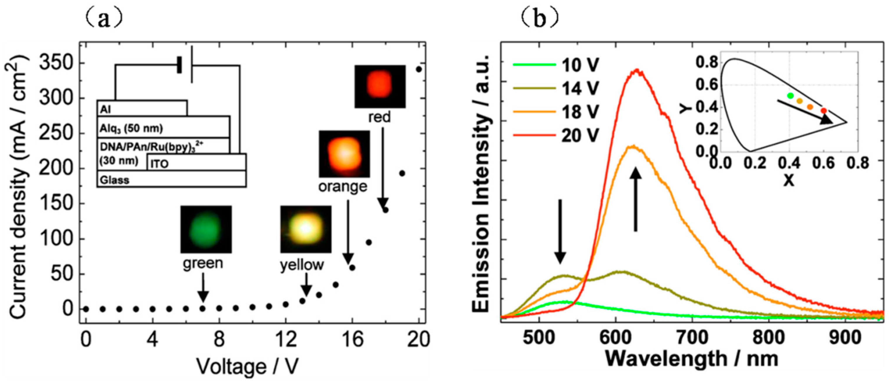
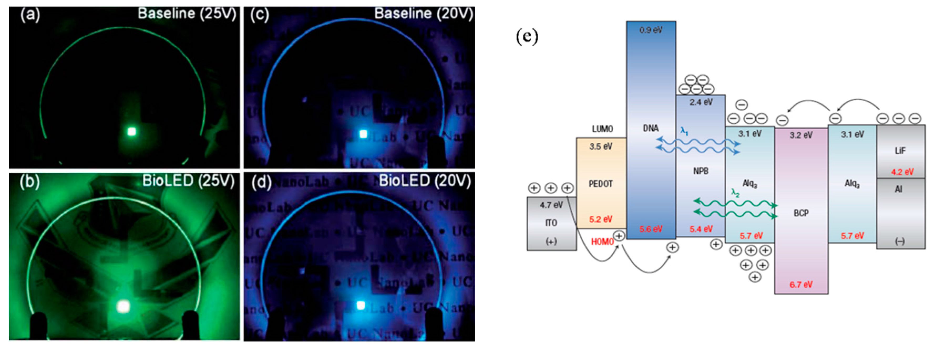
4. DNA for Other Optical Electronic Devices
5. Conclusions
Acknowledgments
Author Contributions
Conflicts of Interest
References
- Mihai, I.-V.; Troshin, P.A.; Reisinger, M.; Shmygleva, L.; Kanbur, Y.; Schwabegger, C.; Bodea, M.; Reinhard, S. Biocompatible and biodegradable materials for organic field-effect transistors. Adv. Funct. Mater. 2010, 20, 4069–4076. [Google Scholar]
- Mihai, I.-V.; Troshin, P.A.; Reisinger, M. Environmentally sustainable organic field effect transistors. Org. Electron. 2010, 11, 1974–1990. [Google Scholar]
- Magliulo, M.; Manoli, K.; Macchia, E.; Palazzo, G.; Torsi, L. Tailoring functional interlayers in organic field-effect transistor biosensors. Adv. Mater. 2015, 27, 7528–7551. [Google Scholar] [CrossRef] [PubMed]
- Dezieck, A.; Acton, O.; Leong, K.; Oren, E.E.; Ma, H.; Tamerler, C.; Jen, A.K.Y. Threshold voltage control in organic thin film transistors with dielectric layer modified by a genetically engineered polypeptide. Appl. Phys. Lett. 2010, 97, 013307. [Google Scholar] [CrossRef]
- Wu, G.; Feng, P.; Wan, X.; Zhu, L.; Shi, Y.; Wan, Q. Artificial synaptic devices based on natural chicken albumen coupled electric-double-layer transistors. Sci. Rep. 2016, 6, 1–9. [Google Scholar] [CrossRef] [PubMed]
- Liao, C.; Yan, F. Organic semiconductors in organic thin-film transistor-based chemical and biological sensors. Polym. Rev. 2013, 53, 352–406. [Google Scholar] [CrossRef]
- Kim, T.-W.; Choi, H.; Oh, S.-H.; Wang, G.; Kim, D.-Y.; Hwang, H.; Lee, T. Hybrid nonvolatile memory devices: One transistor–one resistor devices for polymer non-volatile memory applications. Adv. Mater. 2009, 21, 2497–2500. [Google Scholar] [CrossRef]
- Lim, S.C.; Kim, S.H.; Lee, J.H.; Yu, H.Y.; Park, Y.; Kim, D.; Zyung, T. Organic thin-film transistors on plastic substrates. Mater. Sci. Eng. B 2005, 121, 211–215. [Google Scholar] [CrossRef]
- Tanaka, K.; Okahata, Y. A DNA−lipid complex in organic media and formation of an aligned cast film. J. Am. Chem. Soc. 1996, 118, 10679. [Google Scholar] [CrossRef]
- Heckman, E.M.; Grote, J.G.; Hopkins, F.K.; Yaney, P.P. Performance of an electro-optic waveguide modulator fabricated using a deoxyribonucleic-acid-based biopolymer. Appl. Phys. Lett. 2006, 89, 181116. [Google Scholar] [CrossRef]
- Zhou, J.; Wang, Z.Y.; Yang, X.; Wong, C.-Y.; Pun, E.Y.B. Fabrication of low-loss, single-mode-channel waveguide with DNA–CTMA biopolymer by multistep processing technology. Opt. Lett. 2010, 35, 1512–1514. [Google Scholar] [CrossRef] [PubMed]
- Leonetti, M.; Sapienza, R.; Ibisate, M.; Conti, C.; López, C. Optical gain in DNA-DCM for lasing in photonic materials. Opt. Lett. 2009, 34, 3764–3766. [Google Scholar] [CrossRef] [PubMed]
- Yu, Z.; Li, W.; Hagen, J.A.; Zhou, Y.; Klotzkin, D.; Grote, J.G.; Steckl, A.J. Photoluminescence and lasing from deoxyribonucleic acid (DNA) thin films doped with sulforhodamine. Appl. Opt. 2007, 46, 1507–1513. [Google Scholar] [CrossRef] [PubMed]
- Sznitko, L.; Mysliwiec, J.; Karpinski, P.; Palewska, K.; Parajiniuk, K.; Barkiewicz, S.; Rau, I.; Kajzar, F.; Miniewicz, A. Biopolymer based system doped with nonlinear optical dye as a medium for amplified spontaneous emission and lasing. Appl. Phys. Lett. 2011, 99, 031107. [Google Scholar] [CrossRef]
- Wanapun, D.; Hall, V.J.; Begue, N.J.; Grote, J.G.; Simpson, G.J. DNA-based polymers as chiral templates for second-order nonlinear optical materials. ChemPhysChem 2009, 10, 2674–2678. [Google Scholar] [CrossRef] [PubMed]
- Singh, B.; Sariciftci, N.S. Bio-organic-semiconductor-field-effect-transistor based on deoxyribonucleic acid gate dielectric. J. App. Phys. 2006, 100, 024514. [Google Scholar] [CrossRef]
- Liang, L.; Mitsumura, Y.; Nakamura, K.; Uemura, S.; Kamata, T.; Kobayashi, N. The effect of DNA chain length and chemical structure of the surfactant molecule on the properties of the DNA-based bio-organic field effect transistor memory. J. Korean Soc. Imaging Sci. Technol. 2012, 18, 16–24. [Google Scholar]
- Liang, L.; Nakamura, K.; Uemura, S.; Kamata, T.; Kobayashi, N. Structure of DNA-octadecyltrimethylammonium chloride biopolymer complex and the application to non-volatile BiOTFT memory. Sci. Adv. Mater. 2014, 6, 1516–1519. [Google Scholar] [CrossRef]
- Liang, L.; Mitsumura, Y.; Nakamura, K.; Uemura, S.; Kamata, T.; Kobayashi, N. Temperature dependence of transfer characteristics of OTFT memory based on DNA–CTMA gate dielectric. Org. Electron. 2016, 28, 294–298. [Google Scholar] [CrossRef]
- Feng, L.; Jiang, C.; Ma, H.; Guo, X.; Nathan, A. All ink-jet printed low-voltage organic field-effect transistors on flexible substrate. Org. Electron. 2016, 38, 186–192. [Google Scholar] [CrossRef]
- Facchetti, A.; Yoon, M.-H.; Marks, T.J. Gate dielectrics for organic field-effect transistors: New opportunities for organic electronics. Adv. Mater. 2005, 17, 1705–1725. [Google Scholar] [CrossRef]
- Uemura, S.; Yoshida, M.; Hoshino, S.; Kodzasa, T.; Kamata, T. Investigation for surface modification of polymer as an insulator layer of organic FET. Thin Solid Film 2003, 438, 378–381. [Google Scholar] [CrossRef]
- Chang, J.-W.; Wang, C.-G.; Huang, C.-Y.; Tsai, T.-D.; Guo, T.-F.; Wen, T.-C. Chicken albumen dielectrics in organic field-effect transistors. Adv. Mater. 2011, 23, 4077–4081. [Google Scholar] [CrossRef] [PubMed]
- Kim, S.-J.; Jeon, D.-B.; Park, J.-H.; Ryu, M.-K.; Yang, J.-H.; Hwang, C.-S.; Kim, G.-H.; Yoon, S.-M. Nonvolatile memory thin-film transistors using biodegradable chicken albumen gate insulator and oxide semiconductor channel on eco-friendly paper substrate. ACS Appl. Mater. Interfaces 2015, 7, 4869–4874. [Google Scholar] [CrossRef] [PubMed]
- Hung, Y.-C.; Hsu, W.-T.; Lin, T.-Y.; Fruk, L. Photoinduced write-once read-many-times memory device based on DNA biopolymer nanocomposite. Appl. Phys. Lett. 2011, 99, 253301. [Google Scholar] [CrossRef]
- Wang, Y.; Yan, X.; Dong, R. Organic memristive devices based on silver nanoparticles and DNA. Org. Electron. 2014, 15, 3476–3481. [Google Scholar] [CrossRef]
- Yukimoto, T.; Uemura, S.; Kamata, T.; Nakamura, K.; Kobayashi, N. Non-volatile transistor memory fabricated using DNA and eliminating influence of mobile ions on electric properties. J. Mater. Chem. C 2011, 21, 15575. [Google Scholar] [CrossRef]
- Stadler, P.; Oppelt, K.; Singh, T.B.; Grote, J.G.; Schwdiauer, R.; Bauer, S.; Brezina, H.P.; Bauerle, D.; Sariciftci, N.S. Organic field-effect transistors and memory elements using deoxyribonucleic acid (DNA) gate dielectric. Org. Electron. 2007, 8, 648–654. [Google Scholar] [CrossRef]
- Kim, Y.S.; Jung, K.W.; Lee, U.R.; Kim, K.H.; Hoang, M.H.; Jin, J.I.; Choi, D.H. High-mobility bio-organic field effect transistors with photoreactive DNAs as gate insulators. Appl. Phys. Lett. 2010, 96, 103307. [Google Scholar] [CrossRef]
- Yumusak, C.; Singh, T.B.; Sariciftci, N.S.; Grote, J.G. Bio-organic field effect transistors based on crosslinked deoxyribonucleic acid (DNA) gate dielectric. Appl. Phys. Lett. 2009, 95, 263304. [Google Scholar] [CrossRef]
- Shi, W.; Yu, Y.; Huang, W.; Zheng, Y. The effect of active antennas on the hot-restrike of high intensity discharge lamps. J. Phys. D Appl. Phys. 2014, 47, 205402. [Google Scholar] [CrossRef]
- Shi, W.; Han, S.; Huang, W.; Yu, J. High mobility organic field-effect transistor based on water-soluble deoxyribonucleic acid via spray coating. App. Phys. Lett. 2015, 106, 043303. [Google Scholar] [CrossRef]
- Zhang, Y.; Zalar, P.; Kim, C.; Collins, S.; Bazan, G.C.; Nguyen, T.-Q. DNA Interlayers Enhance Charge Injection in Organic Field-Effect Transistors. Adv. Mater. 2012, 24, 4255–4265. [Google Scholar] [CrossRef] [PubMed]
- Lee, S.-M.; Cho, Y.; Kim, D.-Y.; Chae, J.-S.; Choi, K.C. Enhanced Light Extraction from Mechanically Flexible, Nanostructured Organic Light-Emitting Diodes with Plasmonic Nanomesh Electrodes. Adv. Opt. Mater. 2015, 3, 1240–1247. [Google Scholar] [CrossRef]
- Wallace, C.H.C.; Chan, W.K.; Yuan, Y. Recent Advances in Transition Metal Complexes and Light-Management Engineering in Organic Optoelectronic Devices. Adv. Mater. 2014, 26, 5368–5399. [Google Scholar]
- Kim, J.-B.; Lee, J.-H.; Moon, C.-K.; Kim, S.-Y.; Kim, J.-J. Highly enhanced light extraction from surface plasmonic loss minimized organic light-emitting diodes. Adv. Mater. 2013, 25, 3571–3577. [Google Scholar] [CrossRef] [PubMed]
- Braga, D.; Erickson, N.C.; Renn, M.J.; Holmes, R.J.; Frisbie, C.D. High-Transconductance Organic Thin-Film Electrochemical Transistors for Driving Low-Voltage Red-Green-Blue Active Matrix Organic Light-Emitting Devices. Adv. Funct. Mater. 2012, 22, 1623–1631. [Google Scholar] [CrossRef]
- Bian, C.; Wang, Q.; Ran, Q.; Liu, X.; Fan, J.; Liao, L. New carbazole-based bipolar hosts for efficient blue phosphorescent organic light-emitting diodes. Org. Electron. 2018, 52, 138–145. [Google Scholar] [CrossRef]
- Song, H.-J.; Han, J.; Lee, G.; Sohn, J.; Kwon, Y.; Choi, M.; Lee, C. Enhanced light out-coupling in OLED employing thermal-assisted, self-aggregated silver nano particles. Org. Electron. 2018, 52, 230–236. [Google Scholar] [CrossRef]
- Tang, C.W.; Vanslyke, S.A. Organic electroluminescent diodes. Appl. Phys. Lett. 1987, 51, 913–915. [Google Scholar] [CrossRef]
- Burroughes, J.H.; Bradley, D.C.; Brown, D.A.R. Light-emitting diodes based on conjugated polymers. Nature 1990, 347, 539–541. [Google Scholar] [CrossRef]
- Zalar, P.; Kamkar, D.; Naik, R.; Ouchen, F.; Grote, J.G.; Bazan, G.C.; Nguyen, T.-Q. DNA electron injection interlayers for polymer light-emitting diodes. J. Am. Chem. Soc. 2011, 133, 11010. [Google Scholar] [CrossRef] [PubMed]
- Grykien, R.; Luszczynska, B.; Glowacki, I.; Ulanski, J.; Kajzar, F.; Zgarian, R.; Rau, I. A significant improvement of luminance vs current density efficiency of a BioLED. Opt. Mater. 2014, 36, 1027–1033. [Google Scholar] [CrossRef]
- Gomez, E.F.; Venkatraman, V.; Grote, J.G.; Steckl, A.J. Exploring the Potential of Nucleic Acid Bases in Organic Light Emitting Diodes. Adv. Mater. 2015, 27, 7552–7562. [Google Scholar] [CrossRef] [PubMed]
- Gomez, E.F.; Venkatraman, V.; Grote, J.G.; Steckl, A.J. DNA bases thymine and adenine in bio-organic light emitting diodes. Sci. Rep. 2014, 4, 7105. [Google Scholar] [CrossRef] [PubMed]
- Hagen, J.A.; Li, W.; Steckl, A.J. Enhanced emission efficiency in organic light-emitting diodes using deoxyribonucleic acid complex as an electron blocking layer. App. Phys. Lett. 2006, 88, 171109. [Google Scholar] [CrossRef]
- Reddy, M.S.P.; Park, C. Bright luminescence from pure DNA-curcumin–based phosphors for bio hybrid light-emitting diodes. Sci. Rep. 2016, 6, 32306. [Google Scholar] [CrossRef] [PubMed]
- Nakamura, K.; Ishikawa, T.; Nishioka, D.; Ushikubo, T.; Kobayashi, N. Color-tunable multilayer organic light emitting diode composed of DNA complex and tris(8-hydroxyquinolinato)aluminum. App. Phy. Lett. 2010, 97, 193301. [Google Scholar] [CrossRef]
- Jayme, C.C.; Kanicki, J.; Kajzar, F.; Nogueira, A.F.; Pawlicka, A. Influence of DNA and DNA-PEDOT: PSS on dye sensitized solar cell performance. Mol. Cryst. Liq. Cryst. 2016, 627, 38. [Google Scholar] [CrossRef]
- Dagar, J.; Scarselli, M.; Crescenzi, M.D.; Brown, T.M. Solar cells incorporating water/alcohol-soluble electron-extracting DNA nanolayers. ACS Energy Lett. 2016, 1, 510. [Google Scholar] [CrossRef]
- Yusoff, A.; Bin Mohd, R.; Kim, J.; Jang, J.; Nazeeruddin, M.K. New horizons for perovskite solar cells employing DNA–CTMA as the hole-transporting material. ChemSusChem 2016, 9, 1736. [Google Scholar] [CrossRef] [PubMed]
- Kumar, C.V.; Novak, M.J.; Benson, K.R.; Baveghems, C.; Thilakarathne, V.K.; Stromera, B.S.; Rossa, F.M. Toward the design of bio-solar cells: High efficiency cascade energy transfer among four donor–acceptor dyes self-assembled in a highly ordered protein–DNA matrix. RSC Adv. 2015, 5, 72416. [Google Scholar] [CrossRef]
- Ensslen, P.; Gärtner, M.S.S.; Glaser, K.; Colsmann, A.; Wagenknecht, A. A DNA–fullerene conjugate as a template for supramolecular chromophore assemblies: Towards DNA-based solar cells. Angew. Chem. Int. Ed. 2016, 55, 1904–1908. [Google Scholar] [CrossRef] [PubMed]


| PC70BM (p-Type) | BTDPP2 (Ambipolar Type) | |||||
|---|---|---|---|---|---|---|
| μlin [cm2/Vs] | μsat [cm2/Vs] | Vth [V] | μlin [cm2/Vs] | μsat [cm2/Vs] | Vth [V] | |
| With DNA | 1.7 × 10⁻² | 1.6 × 10⁻² | 10 | 2.3 × 10⁻³ | 1.1 × 10⁻² | 6.5 |
| Without DNA | 7.5 × 10⁻³ | 9 × 10⁻³ | 16 | 4.8 × 10⁻⁴ | 4.4 × 10⁻³ | 12 |
© 2018 by the authors. Licensee MDPI, Basel, Switzerland. This article is an open access article distributed under the terms and conditions of the Creative Commons Attribution (CC BY) license (http://creativecommons.org/licenses/by/4.0/).
Share and Cite
Liang, L.; Fu, Y.; Wang, D.; Wei, Y.; Kobayashi, N.; Minari, T. DNA as Functional Material in Organic-Based Electronics. Appl. Sci. 2018, 8, 90. https://doi.org/10.3390/app8010090
Liang L, Fu Y, Wang D, Wei Y, Kobayashi N, Minari T. DNA as Functional Material in Organic-Based Electronics. Applied Sciences. 2018; 8(1):90. https://doi.org/10.3390/app8010090
Chicago/Turabian StyleLiang, Lijuan, Yabo Fu, Dongdong Wang, Yen Wei, Norihisa Kobayashi, and Takeo Minari. 2018. "DNA as Functional Material in Organic-Based Electronics" Applied Sciences 8, no. 1: 90. https://doi.org/10.3390/app8010090
APA StyleLiang, L., Fu, Y., Wang, D., Wei, Y., Kobayashi, N., & Minari, T. (2018). DNA as Functional Material in Organic-Based Electronics. Applied Sciences, 8(1), 90. https://doi.org/10.3390/app8010090