1. Introduction
The global Internet Protocol (IP) traffic is increasing at incredible rates: Cisco projected that global mobile traffic will increase from 3.7 exabytes per month to 30.6 exabytes per month in 2020 [
1] and there are no signs that this trend will stop anytime soon [
2]. It is not easy to predict implications of this trend in data transmission, but it is clear that Internet traffic is evolving from a relatively steady stream traffic to a more dynamic traffic pattern [
3]. New bursty types of packet-based traffic require network flexibility and reconfigurability at a high-speed, as well as high connectivity at low power consumption. This scenario, however, is not sustainable through packet routing and switching in the electronic domain only. Hybrid solutions have been proposed for decades now [
4]: photonic hardware is introduced for massive-bandwidth data transport and switching, while routing is handled at more modest GHz rates in the electronic domain.
Planar integrated photonic circuits offer an exciting opportunity to create single chip switching solutions for high capacity packet-compliant data routing [
5], since they can potentially reduce the high costs and delays associated with opto-electronic conversion and electronic de/serialization. In the last ten years photonic technologies have quickly matured to the point that an increasing number of components per chip up to few thousands has been demonstrated for function diversity and sophistication [
6,
7,
8,
9] in the optical communication field where requirements are more severe and urgent. However, further scalability must be ensured to provide the requested connectivity in future optical switching engines, while maintaining high performance.
In this work, the progress made in electronically actuated monolithic switching circuits based on the use of semiconductor optical amplifiers (SOAs) is reviewed, focusing on circuit-level functionality. After reviewing the integration technologies that have enabled high-connectivity routing in planar optoelectronic circuits in
Section 2, we focus on circuits that exploit the indium phosphide (InP) integrated photonics platform. In particular, in
Section 3 we address broadband implementations with connectivity of up to sixteen ports in a packet-compliant SOA multi-stage switching matrix. A comprehensive study of the circuit-level gain, loss, and noise performance provides insight into the future scalability of these circuits. In
Section 4, the opportunity of scaling connectivity by combining monolithically integrated wavelength- and space-selective elements is described, including demonstrations of packet time-scale reconfigurability. Opportunities for developing a distributed network for intra-chip monitoring and equalization for next generation photonic circuits are discussed in
Section 5. In
Section 6 we introduce a complementary matrix topology based on resonant elements as developed in the same platform to provide a route for power efficient switching. The strategies for improvements and challenges for future deployment of large-scale fast re-configurable power efficient switch matrices are discussed all over the sections, by looking at figures like connectivity, performance, power consumption, distributed on-chip optical monitoring, and interconnectivity.
2. Monolithically Integrated Fast Optical Switching
Despite the considerable number of concepts and devices proposed and demonstrated over the years, only a relatively small number of integrated switches have scaled to tens of ports. Three-dimensional (3D) microelectromechanical systems (MEMS) have scaled up to hundreds of ports with low (~2 dB) insertion loss and very low power consumption [
10]. However, commercially-deployed optical switching engines using MEMS technologies are unwieldy and too slow for future packet-based networking. It is therefore increasingly important to identify scalable optical switching engines which are capable of fast nanosecond-timescale reconfiguration. Photonic integrated circuits can offer an exciting and viable solution for creating a single-chip switching solution for high-capacity data routing. As a notable example, planar integrated MEMS have been deployed in combination with silicon photonics planar circuits to create up to 64 × 64 photonic switch matrices [
11]: An electrostatically actuated MEMS waveguide is moved to enable a directional coupling between the input and output buses. These waveguides are low-loss and broadband, with a compact footprint, although the actuation voltages of tens of volts are still relatively challenging and a sub-microsecond switching time is set by the intrinsically limiting mechanical movement.
InP integrated photonics offers high performance amplifiers, switches, modulators, detectors, and de/multiplexers in the same wafer scale process. High speed switch elements have primarily used interferometric and gated switch elements that exploit the InP integrated photonics platform. Interferometers offer the potential for low-current and therefore low-power operation. Considerable work focusing on the use of directional couplers, Y-branch couplers, and Mach-Zehnder interferometers (MZI) has been done. The latter have been configured as 2 × 2 elements in the larger monolithic, multistage 16 × 16 and 32 × 32 switch matrices on LiNbO
3 [
12,
13,
14]. More recently, 8 × 8 switch matrices have been fabricated on Silicon-on-Insulator [
15]: Circuit level challenges have focused on improving the modest switch extinction ratios and relaxing the precision requirements for the voltage control. Improved crosstalk and power consumption performance have been achieved using either cascaded Mach-Zehnder interferometers [
16] or by including a short semiconductor optical amplifier gate stage [
17], to the expenses of a higher number of control electrodes. A different approach is provided by the notable example of the 8 × 8 MOTOR circuit, that integrates eight wavelength converters and one cyclic router, offering the prospect of bandwidth reallocations at the optical layer [
18]. However, this class of switch has proved more challenging to integrate.
Semiconductor optical amplifier (SOA) gate switches have been more extensively deployed in system-level studies: Electrical control results are relatively simple and with low voltages; also, tolerance to current variations and excellent crosstalk suppression are typical characteristics [
19]. Furthermore, SOA-based gate switches can enable passbands of several Terahertz, colorless and wavelength multiplexed routing [
20]. System integrators have demonstrated large optical fabrics using multiple stages and planes of discrete components [
21,
22]. These successes have led to a renewed interest in large-scale photonic integration as a route to more flexible and lossless routing systems to reduce system level complexity. As a consequence, in the last ten years, photonic integration technology has evolved rapidly to the point that a number of academic and industry research groups are making more and more complex integrated switching circuits. The first lossless 16 × 16 optical switch matrices were demonstrated by Wang et al. [
23]. The wide-spread use of amplifying waveguides did, however, compromise the dynamic range and increased power consumption per optical path connections. Subsequent work that we have done using active-passive regrown wafer technologies has allowed further enhancements in terms of optical power handling and noise performance [
24]. Moreover, by combining the advantages of high port-count switch fabrics with on-chip wavelength selection [
25,
26], we have demonstrated even further increases in connectivity of up to 64 inputs wavelength channels on a monolithic integrated prototype [
27].
Table 1 summarizes developments in fast SOA-based optical switch matrix technologies for switch sizes of 16 inputs to 16 outputs and above or minimal connectivity of 16 channels. The connectivity is quantified in terms of physical input ports, output ports, and number of unique wavelength specific paths which can be provisioned inside the circuit. These recent developments in switch circuits align approximately to a trend line with a doubling of connectivity in photonics every year [
7] and they will be introduced and described in more details in the next sections.
3. InP SOA-Based Broadband Switch Matrices
Broadband switches are expected to enable considerable energy savings with respect to electronic switching as the line-rate increases, as the data throughput is not directly linked to the actuation energy [
28]. So far, the highest connectivity SOA-gate based circuit has been a three-stage 16 × 16 switch with a hybrid Clos-Tree structure [
23]. A single active epitaxy was used to enable loss-less on-chip operation and 10 Gb/s routing between selected paths. The use of active waveguides for every component within the chip requires significant levels of current injection to overcome loss, and this in turn leads to a building up in spontaneous emission noise and a compromised optical signal to noise ratio (OSNR) of 14.5 dB/0.1 nm. In [
24], we reported the first 16 × 16 switch on a re-grown active-passive epitaxial wafer: The sparse use of SOA gain elements and low loss passive waveguide components is anticipated to allow reduced signal impairment through lower levels of amplified spontaneous emission (ASE) and distortion.
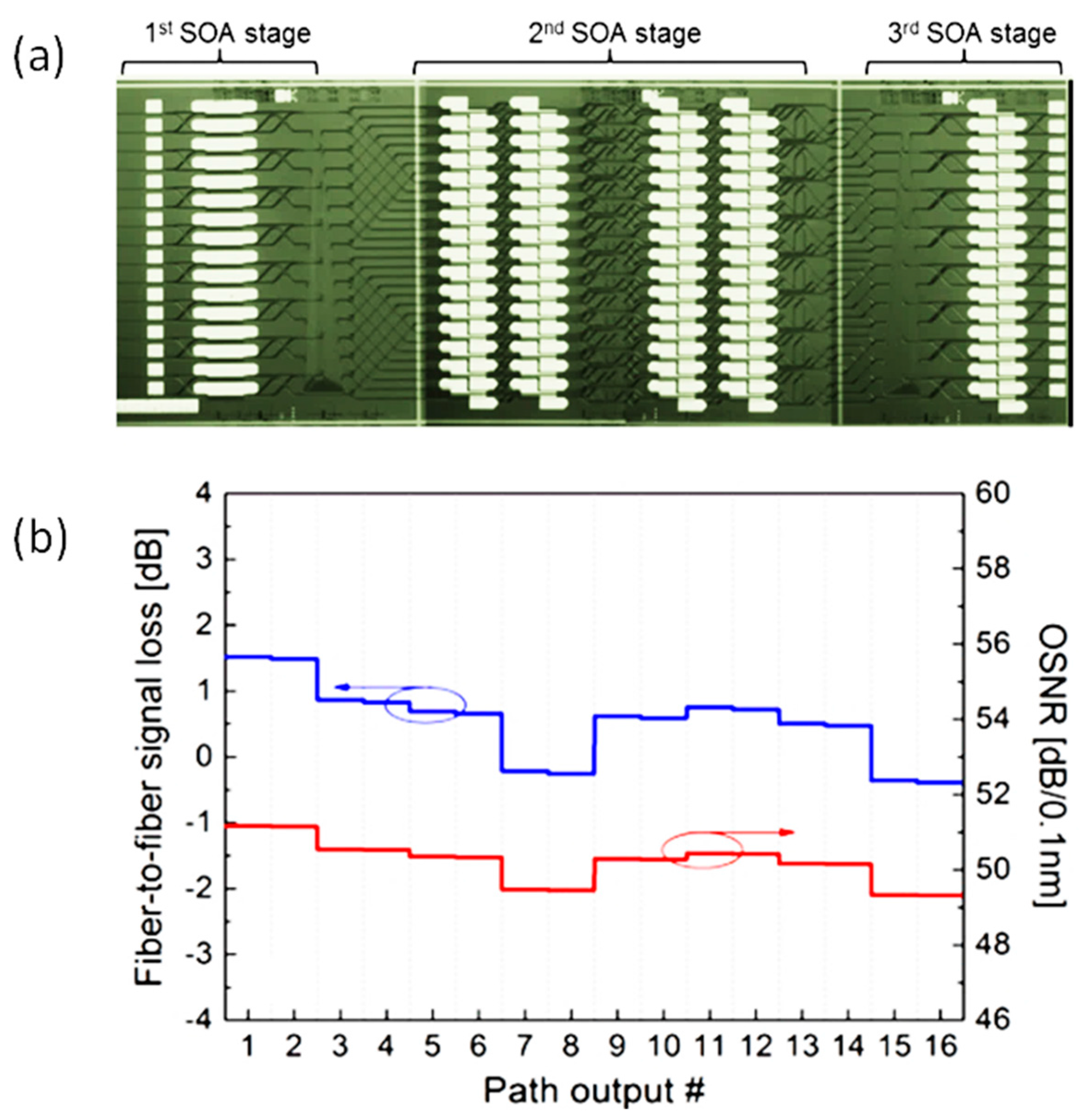
Figure 1a shows the three-stage hybrid Beneš-Tree architecture as implemented with 2 × 2, 4 × 4, and 2 × 2 switches at the input, center, and output stages, respectively. The first and the last stage of SOAs are used as pre-amplifiers and booster amplifiers, respectively. The center stage enables path fast reconfigurability and is replicated in two planes to allow re-arrangeable non-blocking interconnection. The active SOA gates are integrated with the passive broadcast and waveguide routing circuits by using an active-passive epitaxial regrown InP/InGaAsP (Indium Gallium Arsenide Phosphide) wafer. The switch comprises 192,500 μm long SOA gates distributed in six columns and a comparable number of splitters, combiners, and waveguide crossings within a chip area of 4.0 mm × 13.2 mm, for a record number of 480 components on a single photonic chip [
7]. To create the photonic waveguide wiring, a four-step inductively coupled plasma (ICP) etch was performed. While the central SOA electrodes are connected to fast programmable drivers for path reconfiguration, the remaining connections at the inputs and at the outputs are made via electrical patch panels to arrays of modular direct current (DC) sources. Both single and multi-path operation are assessed [
29]. Polarization controllers are used as the circuit is optimized for transverse electric (TE) polarization.
Initial characterization is performed to study the component level and path level operation [
24]: All quoted on-chip losses come from in-situ measurements. Only thirty-two paths have been tested, due to the chip complexity: the paths from input 1 to output 1 to 32, and paths from input 32 to output 1 to 32—these paths include the shortest and the longest paths of the chip for full loss map understanding. Path yield numbers are reported in the next section for a similar area chip, fabricated on the same wafer. The use of low-loss passive waveguides in combination with high-contrast active gates leads to promising system level metrics in terms of optical signal to noise ratio with a best case value of 28 dB/0.1 nm. However, due to the moderate scale of integration, the space switch scheme presents high path losses: The fiber-to-fiber signal losses increase as path length and complexity increase, because of the additional traversed components. The measured total passive losses along the thirty-two paths include an inherent 30 dB loss contribution resulting from the broadcast-select capability and an excess 37 dB loss resulting from component-level imperfections, with a maximum loss variation of 12.8 dB. The gain from the SOA gates can compensate much of the excess component losses, while the inherent losses of about 30 dB coming from the broadcast-enabled architecture are present in any given path. The circuit-level losses were analyzed by evaluating the losses in comparable circuits and through direct measurement. The noise performance was predicted by estimating the optical power map for the signal and noise within the switch matrix circuit and including the additional amplified spontaneous emission noise contributed at each SOA gate. Each of the three stages of the SOA gates in the circuit was expected to operate with a mean gain of 12.9 dB and a mean amplified spontaneous emission power density of −47.3 dBm/0.1 nm. The operating optical input power for the input SOA was −11.6 dBm and for the central and output SOAs was −21 dBm, so the 500-μm-long gates were operated far from the optical saturation power. The electrical bias conditions were 75 mA and 1.5 V. The agreement for the implemented elements is excellent, giving confidence that the loss and noise performance of the circuits can be clearly attributed to the excess losses of the components. The excess losses can, however, be significantly reduced by using optimized components like mode-size adaption at the facets [
30], low-parasitic-reflection splitters [
31], low-loss waveguide crossing through a broadening at the intersecting waveguides [
32], and low waveguide losses of the order of 0.5 dB/cm for minimized p-doping level in the passive waveguides [
33]. The projected performance for the 16 × 16 switch matrix with optimized component losses are shown in
Figure 1b: lossless circuit level operation is enabled and a radical impact on the optical signal to noise ratio is found by being increased up to about 50 dB/0.1 nm. This would correspond to a circuit level noise figure of 13.7 dB, of which 5.3 dB is attributable to losses between the input side fiber and the first SOA gate. This analysis suggests how a further increase in connectivity is possible, but requires careful design of the chain of cascaded SOAs in a multistage optical switch: reduced losses at the input of the first SOA stage can provide improved switch noise figures. Also, the losses per stage must be designed to be balanced by the SOA-gain stage, keeping the SOA far from the saturation point, in a chain of multiple optical amplifiers.
The operating current and voltage per path are currently 240 mA and 1.5 V for the three gates. If an on-chip preamplifier is included for on-chip gain, the operating current (power) is expected to increase to 340 mA (0.55 W/path). A few watts of power consumption is then expected for the fully loaded chip. The temperature is kept at 15 °C by fixing the chip on a temperature-stabilized water-cooled copper mount. When compared with an all-active approach, the active-passive integration scheme enables order-of-magnitude noise performance improvement as well as reduced energy requirement.
This analysis opens a route to broadband switches with connectivity higher than sixteen IOs. Larger level connectivity clearly implies a larger area that is, however, limited not only by the maximum available InP wafer size, but also by the difficulty of a uniform wafer processing. In
Section 7 the author comments on complementary approaches to pursue large-scale integration.
4. Monolithically Integrated InP 8 × 8 Space and Wavelength Selecting Switch
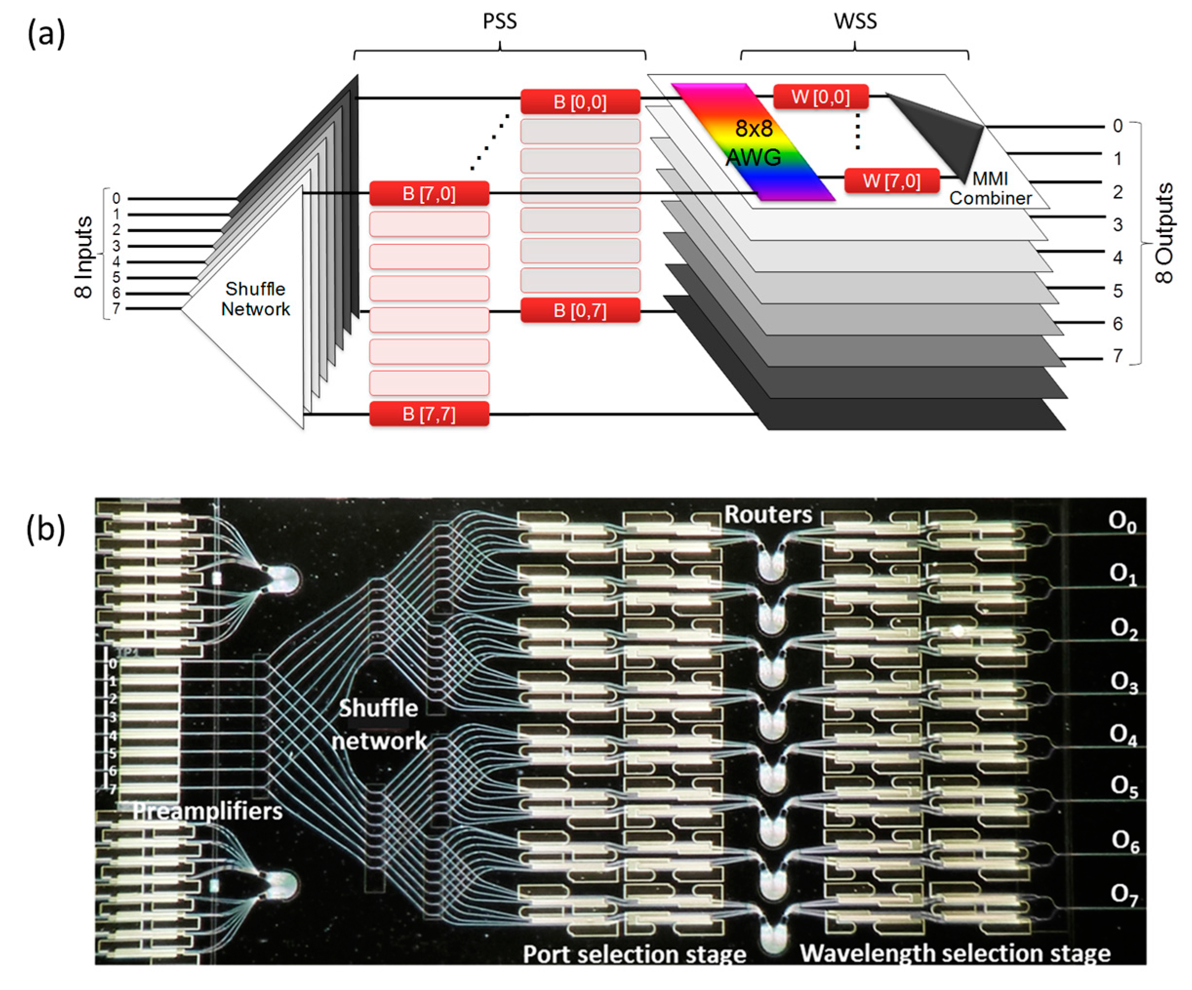
Orders of magnitude increases in reconfigurability become possible when the use of wavelength division multiplexing (WDM) is combined with on-chip wavelength selective routing: The 8 × 8 integrated cross-connect represents an elegant example of an in-plane circuit which provides a connectivity of up to 64 input and output channels [
27]. Here, we perform both space domain switching and wavelength domain channel selection within the same monolithic circuit in order to show the highest level of connectivity and data capacity on a single InP photonic integrated chip. The architecture for broadband photonic and wavelength selective cross-connection is shown in
Figure 2a. The circuit consists of a combination of a broadband photonic switch stage (PSS) for port selection and a wavelength selecting stage (WSS) for color selection, both based on the use of SOAs. Eight colorless WDM input ports connect to an array of pre-amplifying SOAs. Broadcast shuffle networks map each of the inputs to the eight output ports. The first stage of SOA gates is used for input port selection and connects to eight cyclic arrayed waveguide gratings (AWGs). The AWGs route the different wavelength channels to the second stage array of broadband SOAs to perform wavelength selection. Selected channels are aggregated with broadband fan-ins to provide the eight colorless outputs. The grey-scale layers in
Figure 2a are the other seven identical layers implemented in the integrated circuit for both stages. The red boxes are the SOA-gates used in each of the stages.
The device is realized on a re-grown active-passive InGaAsP/InP epitaxy. An optical image of the chip is shown in
Figure 2b. The eight pre-amplified colorless inputs are broadcast through a shuffle network made of cascaded 1 × 2 multimode interferometer (MMI) splitters. After port and color selection, the selected channels are combined with broadcast cascaded 2 × 1 MMI couplers. The active islands in the InP wafer are used for SOA gates and preamplifiers, while the passive regions are used for waveguide wiring, splitters, and cyclic routers. The cyclic AWG used in the WSS is designed with a channel spacing of 3.2 nm (400 GHz) and a free spectral range of 25.6 nm. All input and output waveguides are positioned on a 250 μm pitch to enable simultaneous access to all the ports using a commercially sourced lensed fiber array. The 136 SOA contacts are wire-bonded to an electronic printed circuit board (not shown). The chip is attached with conductive epoxy to a water-cooled block. The total footprint of the switch is 16.4 × 6.7 mm
2. Electrical I-V characteristics are analyzed to identify 126 SOAs with good diode characteristics out of a total of 136. Two fails are attributable to an imperfect lithographic step causing electrode detachment, six are associated with bond-wire detachments, and two are short circuits. From the photonic switching stage to the output side, 432 paths out of 512 paths connections are verified: 84% of the paths from the input to the output side of the chip are electrically and therefore optically connected in this first prototype. Each path includes three SOAs as in the 16 × 16 broadcast switch matrix, but the losses are modest, which indicates a more straightforward route to further scaling. However, in this case the multi-stage switch is characterized by an asymmetric chain of SOAs: Moving to a 16 × 16 cross-connect, for example, implies the introduction of six splitters after the first amplifier which needs to be compensated by a longer second-stage SOA.
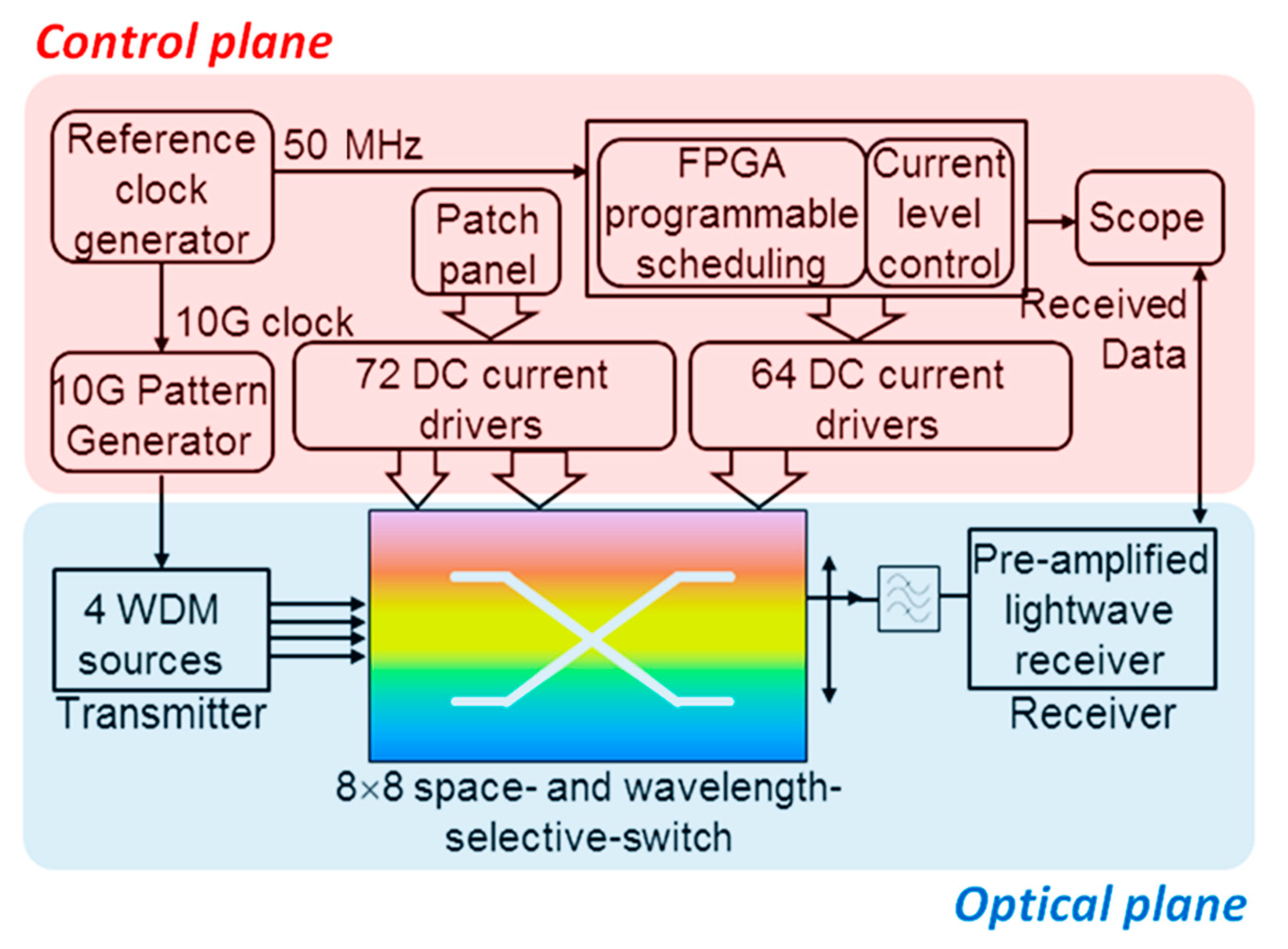
Multi-path WDM 10 Gb/s data routing is demonstrated through the experimental control plane schematically shown in
Figure 3. Very importantly, a common reference clock generator is needed for the programmable logic and the bit error rate test equipment to allow synchronization between the routed data and the switch controller. At the optical plane, four different wavelength channels, λ
0, λ
1, λ
2, and λ
3, with a nominal channel separation of 400 GHz are multiplexed and modulated using a Mach-Zehnder modulator. The WDM signal is then amplified, de-multiplexed, de-correlated, and used as input to the device with 0 dBm channel power. The chip output is connected to a pre-amplified optical receiver after a 0.95 nm bandwidth filter for broadband noise rejection. An average total current per path of the order of 140 mA is used. Optical signal to noise ratios greater than 27.0 dB for 0.1 nm resolution bandwidth and a mean 13.3 dB on-chip loss are measured for each of the channels of a multiplexed channel, as evaluated at a representative path from input 0 to output 0 [
27]. With the maximum number of three SOAs on a single path, no oscillation is observed. When moving to a bigger number of gates, the inclusion of isolation sections may be needed.
The electrical plane comprises fast current drivers and programmable logic. A multiple current source provides DC currents to the pre-amplifying SOAs. Fast current drivers connect to the SOA selector gates of the integrated cross-connect to enable path and channel selection. The current levels for each of the SOA selector gates is separately programmed by means of digital-to-analog converters (DACs) and a central microcontroller. An Altera Stratix III field programmable gate array (FPGA) provides time-slotted control signals to the nanosecond rise-time current drivers for optical path selection. Bit-level synchronization is achieved between the routed data and the switch controller by means of a common reference clock generator between the FPGA and the bit error rate (BER) test equipment.
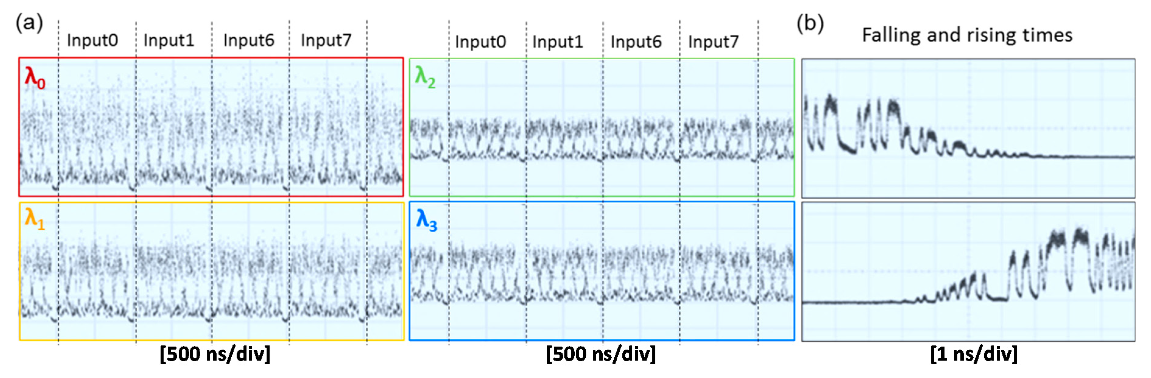
To demonstrate simultaneous WDM multi-path data routing the wavelength multiplexed data is split into four copies using broadband splitters and launched into four input ports: 0, 1, 6, and 7 of the chip. Sixteen channels are routed within the 8 × 8 cross-connect to output port 0. All four input paths are sequentially enabled with a round-robin scheduling and loaded with WDM input signals for dynamic multi-path WDM reconfigurability studies. The correspondent SOAs are driven by periodic 1 µs pulses with 60 ns guard-bands programmed via the FPGA.
Figure 4a shows the time traces of the output WDM signals. Along the x-axis the selected input port changes at each time slot as for the round-robin scheduling. The four sets of wavelengths are selected using external optical filters and are displayed as four separate graphs. The time traces appear to be clean and well resolved. The optical power is levelled for each wavelength to within 2 dB, as the current values have been optimized for equalized output power from time-slot to time-slot.
Figure 4b also shows the fall and rise time for the output signal when moving from one time slot to the next one: The switching occurs within 5 ns [
34]. Power penalty is expected to be dominated by amplified spontaneous emission from the transmitter side amplifier and the cross-connect. For higher input powers and number of wavelengths per channels, new optical amplifier concepts based on low-overlap between the mode and the gain area may prevent unwanted cross-gain modulation.
The requirements for reduced energy use also require the photonic components to be abstracted to enable tractable network level implementations: Multicast capability, packet-time-scale reconfigurability, power levelling irrespective of signal path, distributed signal quality monitoring, and data rate transparency have been implemented at the chip level in order to enable an abstracted digital control plane [
34,
35,
36]. The first investigation on the impact of varied switch loads from unicast to multicast to broadcast on device performance was also performed for this chip [
35]. Electrical power dissipation may be estimated from the mean bias current (50 mA) and the mean voltage across the SOAs (1.2 V). The preamplifiers and wavelength-select stage SOAs are operated continuously and the space-select stages are scheduled. This leads to an electrical input power of 0.78 W for unicast and 2.88 W for broadcast operation. If dynamic scheduling was implemented for the wavelength-select stages as well, a more modest 1.44 W electrical power would be required with only 1 dB gain reduction. Further energy savings are also feasible through optical circuit level optimizations [
34].
5. On-Chip Distributed Power Monitoring
The recent demonstrations of multi-path, multi-wavelength packet scheduling highlight the potential for highly reconfigurable networking with relatively simple control planes, but this places stringent demands on the channel monitoring. So far signal monitoring is being performed at the edge of the network, and is not well adapted for an optical packet paradigm. Distributed optical performance monitoring (OPM) is the key tool for future optical networking. In particular, the optical signal-to-noise ratio (OSNR) monitoring can provide information on the intra-chip signal transmission quality. Intra-chip OSNR measurement has been demonstrated through both discrete [
37] and integrated [
38,
39,
40] solutions, but has never been integrated within a switching circuit. However, the most advanced circuits do already contain the essential components. A combination of SOA gate and AWG technology can provide on-chip integration of active elements and filtering functionality for a more straightforward route to signal and noise detection.
We have recently proposed and demonstrated an OSNR meter co-integrated with the 8 × 8 cross-connect, presented in
Section 4, using switch gates as photo-detectors (PDs), to enable the analysis of signal quality in an integrated packet routing engine [
36]. An electronic pre-calibration scheme is proposed which can be performed before chips are selected for packaging and is done to measure the filtered integrated optical power after the AWGs, which is then used to calculate a noise power spectral density correction factor to be used for the intra-chip OSNR calculation. For the in-service operation, the pre-amplifier is used to compensate fiber-chip coupling of the in-coming signal, and the wavelength-select gates are used again in detector mode to separately measure signal and noise power.
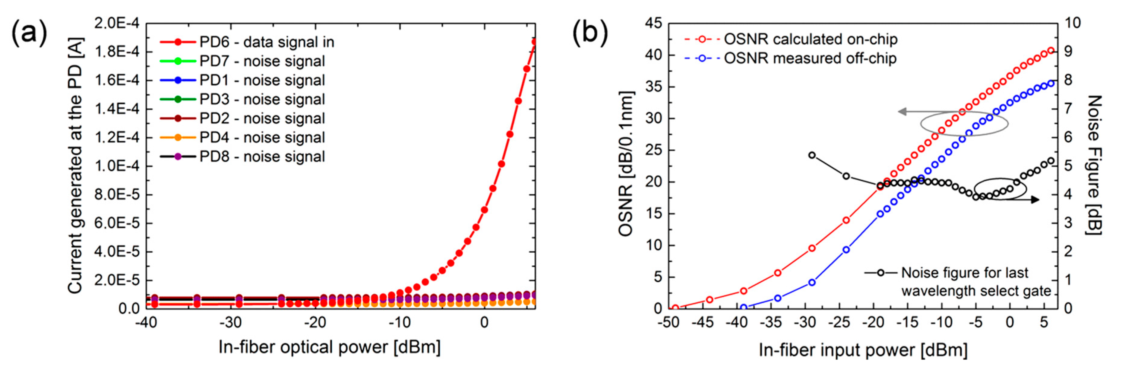
Figure 5a shows the integrated currents measured at all the PDs. The signal level increases exponentially with input power. At low input powers of −30 dBm power, the measured on-chip signal power approaches the integrated in-band noise. This is expected to be dominated by the space-select ASE.
The OSNR is calculated as the ratio between the total integrated current received at the PD6, which is corrected for in-band noise and the appropriately scaled total out-of-band noise contribution. This is plotted as a function of the input power in
Figure 5b. The red curve shows the OSNR versus in-fiber optical input powers: An OSNR dynamic range extending from 6 to 40 dB/0.1 nm is demonstrated. The calculated noise figure of the last SOA gate is also plotted as the difference between the calculated on-chip OSNR and the measured off-chip OSNR.
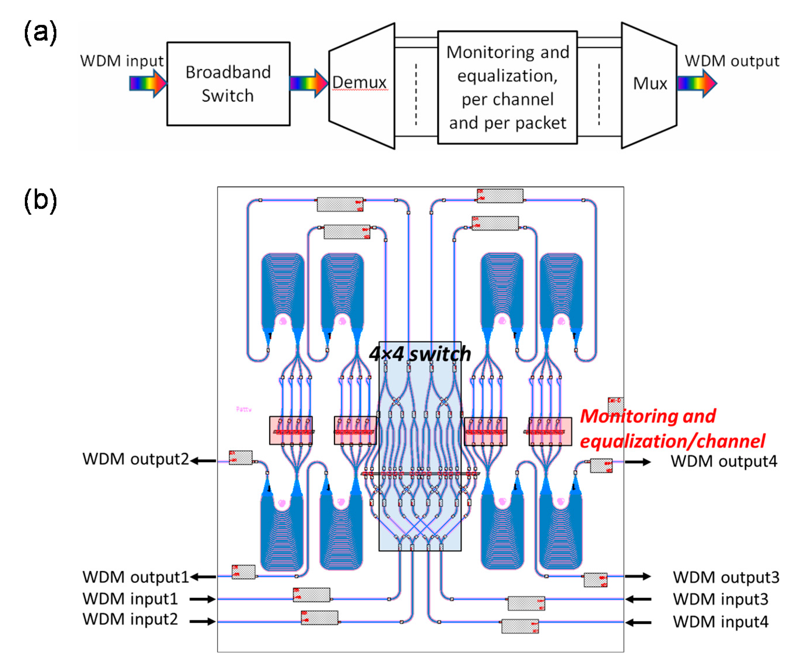
The possibility of providing intra-chip measurement of signal OSNR opens up the opportunity to provide real-time equalization per channel in WDM optical switches: on-chip OSNR and power monitoring per channel increase network awareness at the physical layer and allow for power channel equalization. Concepts of WDM space switches followed by co-integrated channel separation for per-channel monitoring and equalization can become feasible at the packet level. The schematic of the foreseen concept for an aware space switch is displayed in
Figure 6a.
A tentative design for an aware WDM 4 × 4 space switch is shown in
Figure 6b: the light blue box indicates the 4 × 4 space switch and the four pairs of AWGs are for each of the multiplexed channels. The red boxes include the power monitoring, implemented per channel as an integrated 5:95 tap based on a directional coupler design, and an in-line 3 dB SOA-based attenuator, for power adjustment at the chip output. This chip, fabricated on the generic InP technology, takes two die cells of space for a total size of 4.6 × 8 mm
2.
6. InP MRR-Based Switching Cross-Point Matrices
Micro-ring resonator (MRR) elements have been considered extensively, given the increased availability of silicon on insulator technology for photonic circuits. Higher-order ring resonators offer a flattened-passband response that enables wavelength-tolerant, broadband routing in a cross-grid array [
41]. Faster actuation has proven more challenging with cross-point architectures generally because the physical size of the switching elements has largely precluded the use of fast electro-optic switching. One potential exception is the vertically coupled SOA switch [
42]. Recently, we have explored the use of photonic integrated circuits based on ring-resonators on the InP photonics platform. By using InP integrated phase shifters for phase matching and switching activation, these switch matrices provide fast switching and potential low electrical power consumption. Prior work in InP photonics has focused on using first-order micro-ring resonators for this purpose [
43,
44], but higher-order resonators have been shown to decouple bandwidth and the signal extinction implying that both parameters can be optimized individually. As an added incentive, the enhanced bandwidth of such devices also increases their tolerance to variations in fabrication [
41].
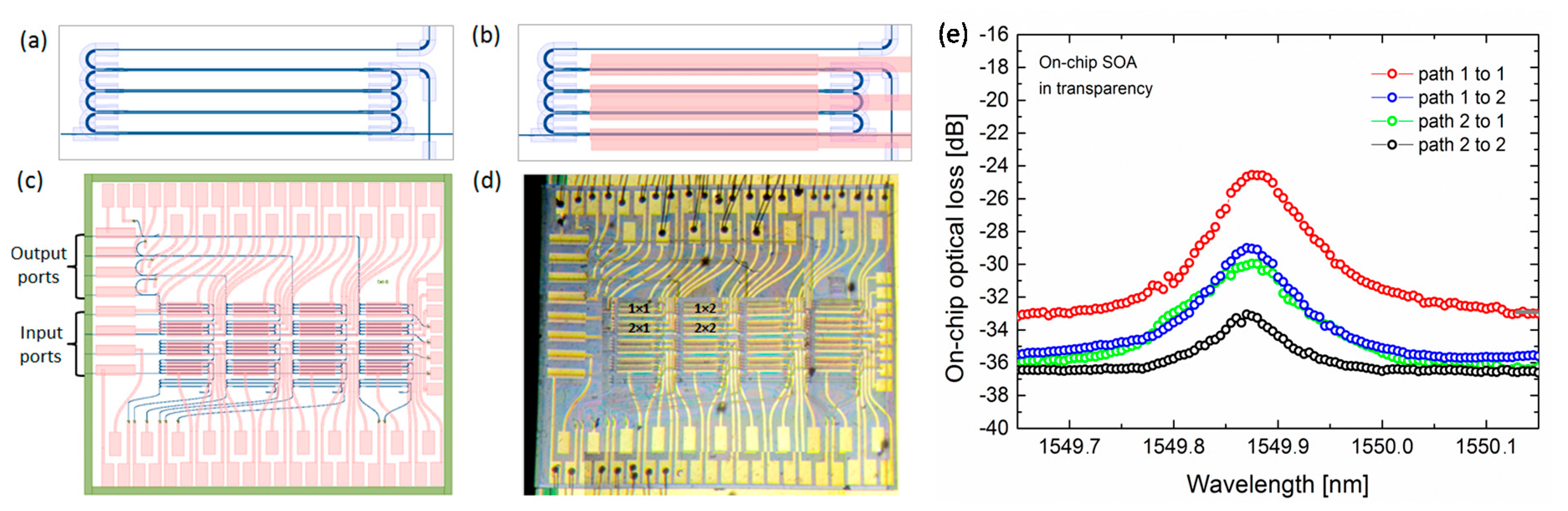
Recently, we have designed and fabricated the first 4 × 4 InP switch matrix based on third-order resonators [
45,
46]: three race-track-like ring resonators are coupled through directional couplers (
Figure 7a). The local refractive index changes due to the electric field and the carrier depletion of a reverse biased junction is used to tune the resonant-based switch elements and represents an attractive power-efficient alternative.
Figure 7b indicates the phase modulator placement. Fast electro-optic tuning at close-spaced phase modulators is used to allow data to drop to the next port or pass through. The matrix is made of sixteen switching elements which are based on these third-order ring resonators. The full mask layout and a photograph of the realized entire switch matrix are shown in
Figure 7c,d, respectively.
The desired coupling coefficients are determined by varying the gap separating the directional couplers, while keeping fixed the coupling lengths. The total chip size is about 4.5 × 3.8 mm
2 and includes 500 µm long SOAs placed after each input-output port to compensate for coupling losses and for power equalization at the optical outputs.
Figure 7e shows the measured spectra for all the four paths. The total 12 dB (2 × 6 dB) fiber-to-chip coupling losses are already subtracted from the plots. All four symbol curves are centered at 1549.87 nm and a 3 dB pass-bandwidth of 11.25 GHz (0.09 nm) is measured for each of the switch elements, which is close to the nominal value. The stop-band part of the higher loss spectra is believed to be limited by the SOA noise. On-state on-chip losses for the single switching element are of the order of 6 dB. To enable high connectivity switching fabrics, smaller and lower-loss switch elements will become important. Techniques to further reduce the on-chip losses are currently being investigated: the use of high resolution lithography is being explored to enable higher density and lower on-chip losses. Moreover, the combination of high precision lithography for shorter couplers, higher efficiency quantum well phase modulators, and the use of all-deep ring resonators, which avoid the need for mode converters, is believed to enable further scaling up to the same order as for SOI ring-resonators based cross-point matrices [
45].
Ten and twenty billion bits per second (10 Gbps and 20 Gbps) data routing is performed across a combination of four different paths in the circuit with error-free operation with a maximum power penalty of 2.6 dB [
47]. The on-state electrical power consumption is recorded to be only 79 µW for the single switch element, which leads to a minimum energy consumption of 8 fJ/s for 10 Gb/s operation, identifying a potential route for energy efficient optical switching. Fast switching of a few nanoseconds for the rise and the falling time is also verified.
7. Discussion
The projected performance of recently realized medium-scale InP photonic fast switching circuits have been presented. This helps in defining the strategies towards large-scale InP photonic integrated circuits (PICs) switches in relation to figures like connectivity, physical layer performance, power consumption, distributed on-chip monitoring, and interconnectivity.
High-radix 4 × 4 SOA-based switch elements have been efficiently configured in multistage networks to enable high connectivity with a limited number of stages, including 2 × 2 SOA-based switches at the input and at the output. Three switch stages provide a good compromise between optical wiring complexity, signal integrity, and control complexity. By using active–passive multi-stage SOA monolithic integration we have enabled switching matrices with up to 480 components, connecting 16 inputs to 16 outputs [
24] (
Figure 1a). This can potentially route massive bandwidth signals independently of signal wavelength and in a number of multiplexed wavelength channels. We have demonstrated that orders of magnitude increases in reconfigurability is possible when the use of wavelength division multiplexing is combined with on-chip wavelength selective routing: The 8 × 8 InP integrated cross-connect provides a connectivity of up to 64 input and output channels [
27] (
Figure 2a). Further increases in connectivity are possible but require careful design of the chain of cascaded SOAs and losses per stage. Also, reduced losses at the input of the first SOA stage must be provided for low signal degradation.
Complementary approaches for achieving large-scale integrated optical switch matrices require a complex mesh of interconnection which is not well supported by single layer waveguides as conceived so far. Further scaling motivates more sophisticated optical wiring. Two strategies for achieving higher connectivity are here highlighted. The InP-Membrane-On-Silicon (IMOS) platform is a photonic integration researching InP-based membranes on top of silicon chips [
48]. This approach represents a valid example of how to shrink size, while retaining gain and enabling future integration on complementary metal-oxide semiconductor (CMOS) circuitry, through a low thermal conductivity polymer layer. Also, monolithic multi-layer InP integration can be used to enable three-dimensional connectivity for large-scale photonic integrated circuits, potentially offering a step change in optical circuit connectivity and removal of crosstalk at the top-bottom waveguide intersections [
49,
50].
As the data throughput is not directly linked to the actuation energy, such broadband switches are expected to enable considerable energy savings as the line-rate increases [
28]. The involved electrical input energy for chip reconfiguration is of the order of a few watts [
24], but further electrical power reduction is desirable. New architectures and technologies must be conceived that provide packet-scale switching functionality while being power efficient. The combination of SOA technology and InP electro-optic effect offers the opportunity of achieving potentially low power consumption and fast switching in photonic integrated circuits based on ring resonators: the first InP third-order ring resonator-based switch matrix fabricated on active-passive integrated InP platform [
45] is characterized by an on-state electrical power consumption of only tens of µW per switch element, which is four order of magnitude lower than in a conventional forward bias SOA-gate. The worst case 6 dB losses between the paths are expected to be dominated by the off-state losses which may be reduced with further building block optimization. The low extinction transfer function might be due to obtained off-target coupling coefficients at the directional couplers, which we believe we can overtake by patterning the circuit through deep- ultraviolet (UV) lithography: higher control of critical dimension losses and reduced sizes switch element are expected to enable lossless operation of cross-point matrices.
The recent demonstrations of multi-path, multi-wavelength packet scheduling highlight the potential for highly reconfigurable networking with relatively simple control planes, but this places stringent demands on the channel monitoring: Distributed optical performance monitoring (OPM) is the key tool for future optical networking. The recently proposed and demonstrated OSNR meter, co-integrated with a photonic integrated switch using switch gates as detectors [
36], opens the route to on-chip networks where it is possible to “sense and act” in order to maintain the signal integrity or to diverge data through a different path.


