
Nonlinear Silicon Photonic Signal Processing Devices for Future Optical Networks


Abstract
:1. Introduction
2. Amorphous Silicon Waveguides
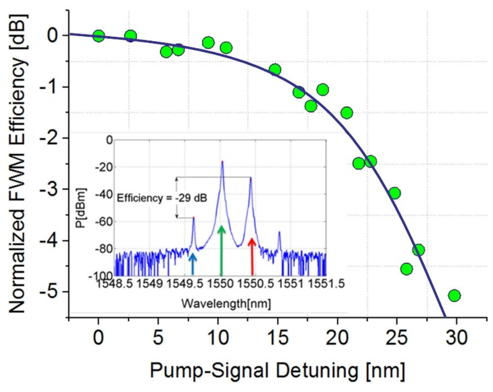
2.1. Linear and Nonlinear Optical Characterization
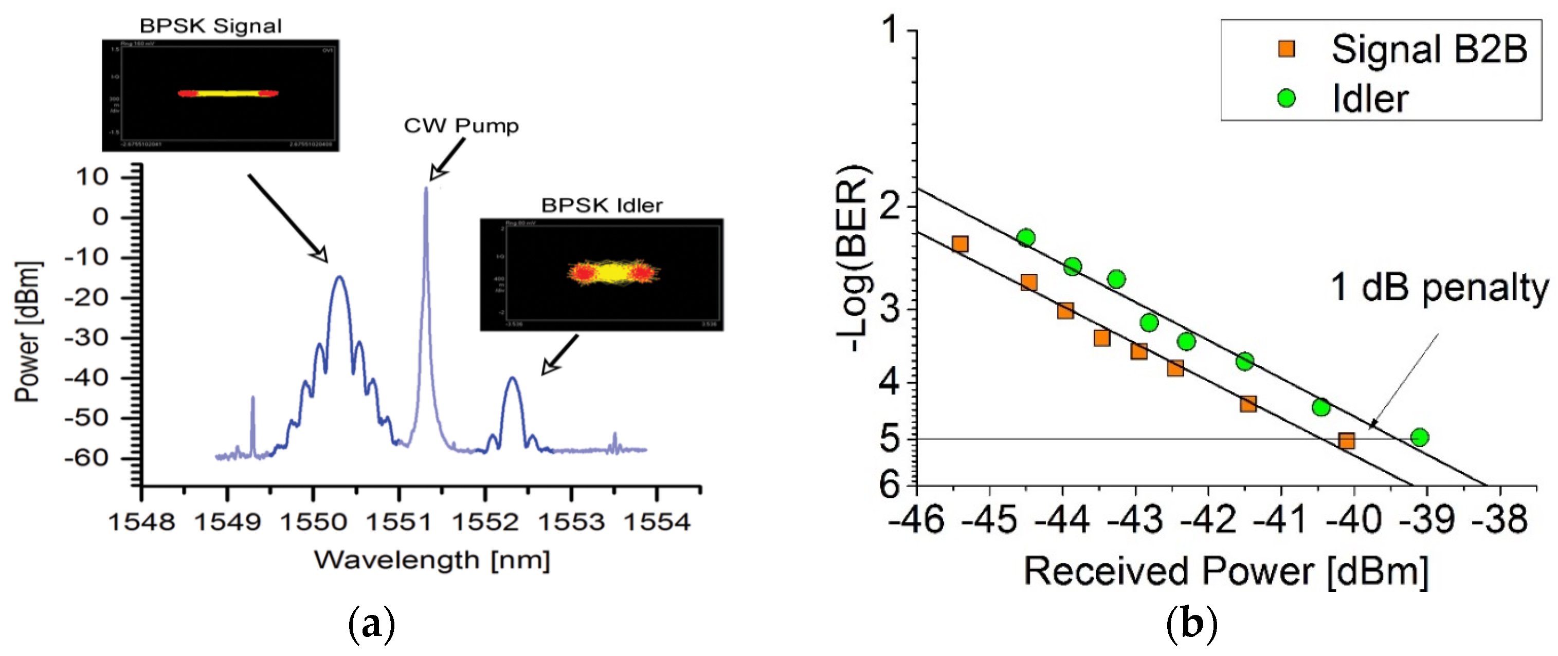
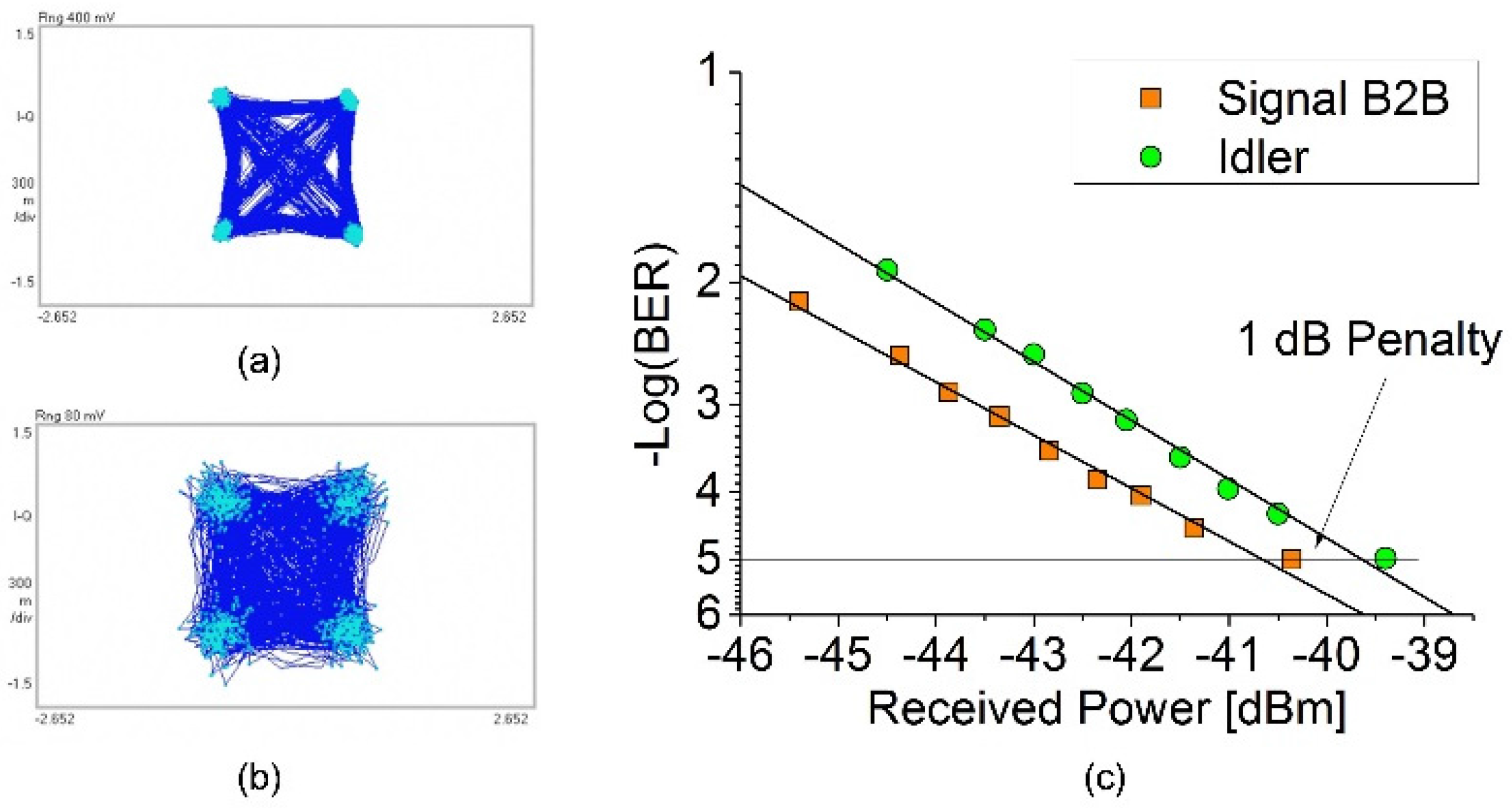
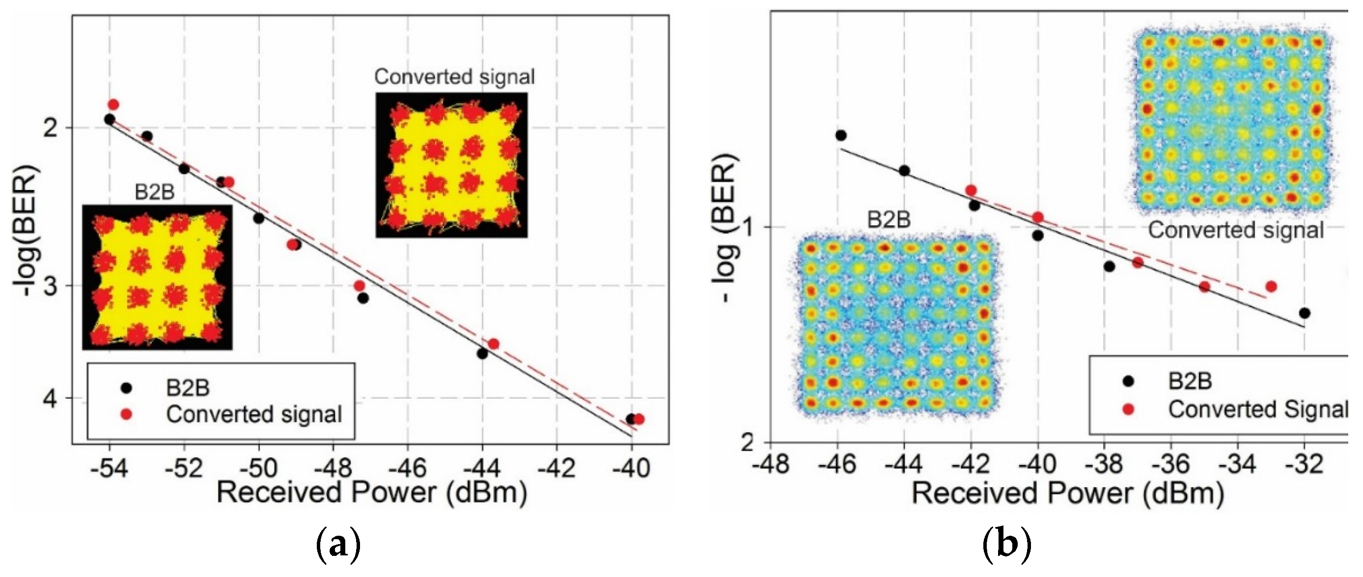
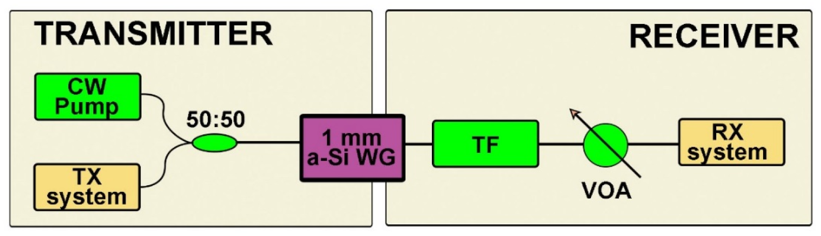
2.2. All Optical Wavelength Conversion of DPSK and QPSK Signals
3. Silicon Germanium Waveguides and Nonlinear Applications
3.1. Linear and Nonlinear Optical Characterization
3.1.1. Linear Loss
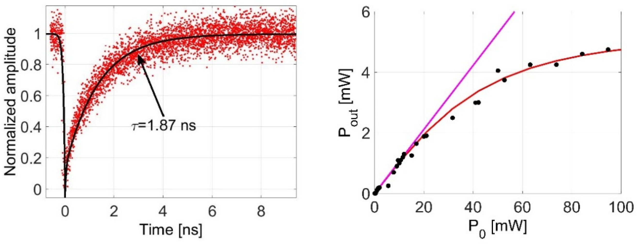
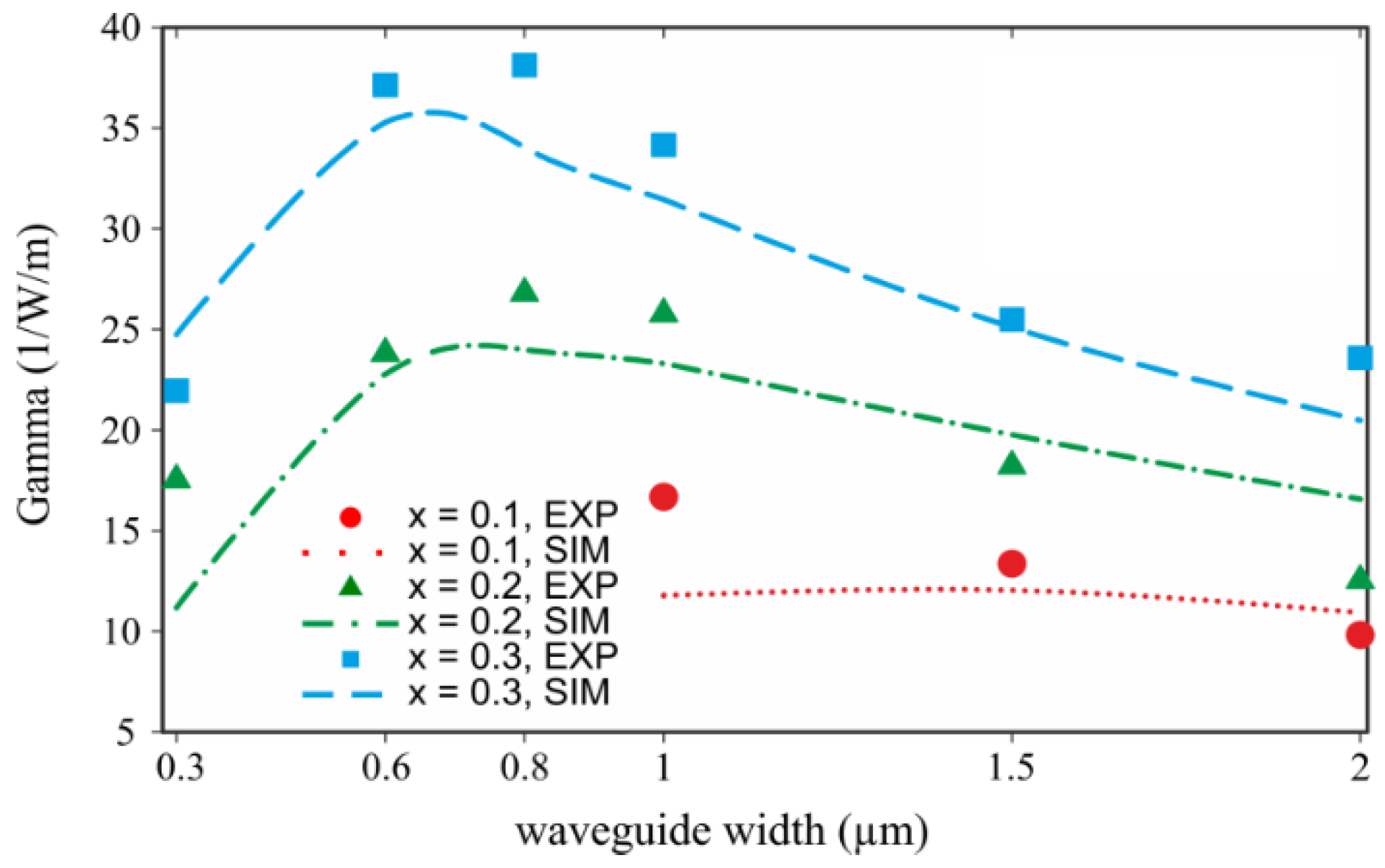
3.1.2. Kerr Nonlinearity
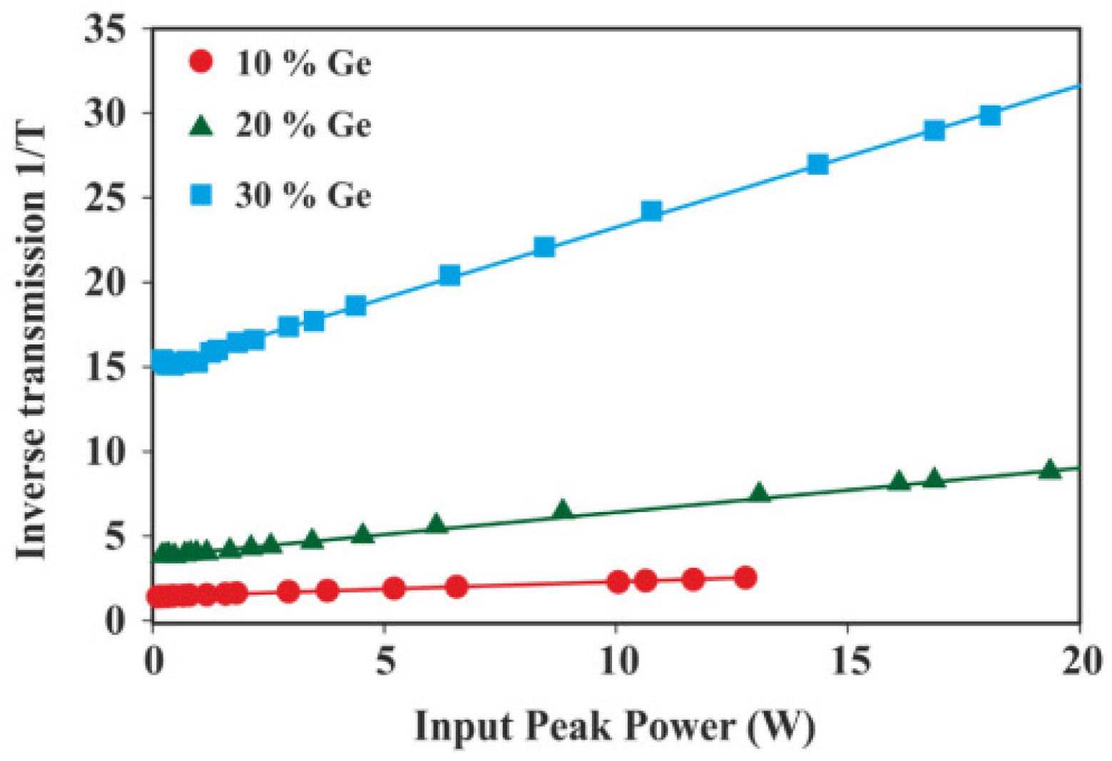
3.1.3. Two-Photon Absorption
3.2. Wavelength Conversion of 16-QAM and 64-QAM Signals:
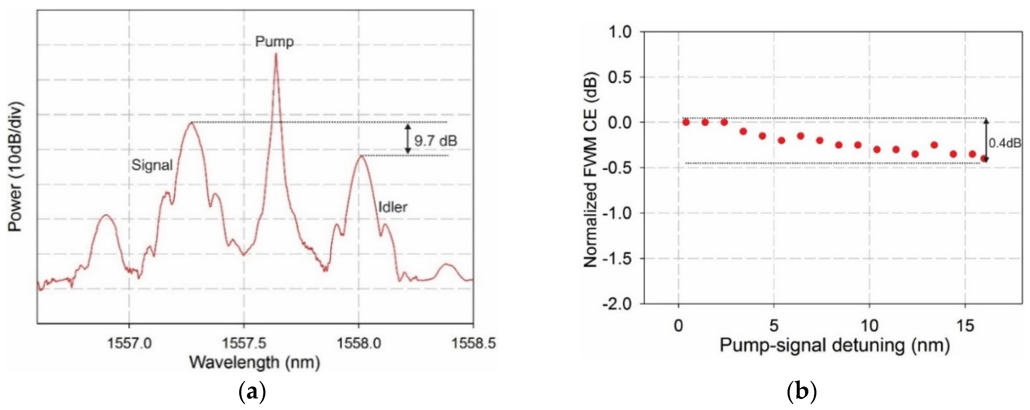
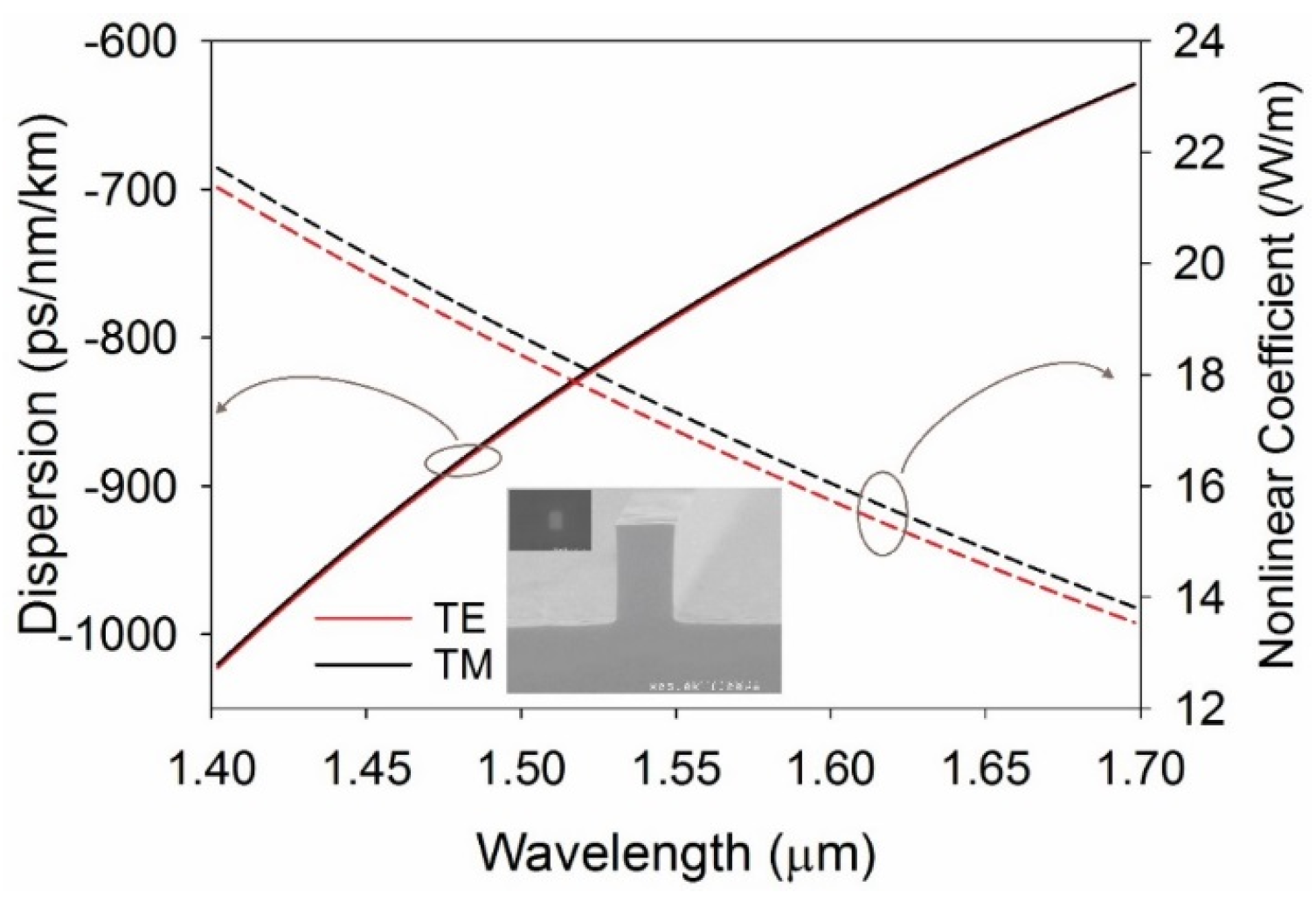
3.3. Low Birefringence SiGe Waveguides
4. Novel Materials for All Optical Processing Nonlinear Devices
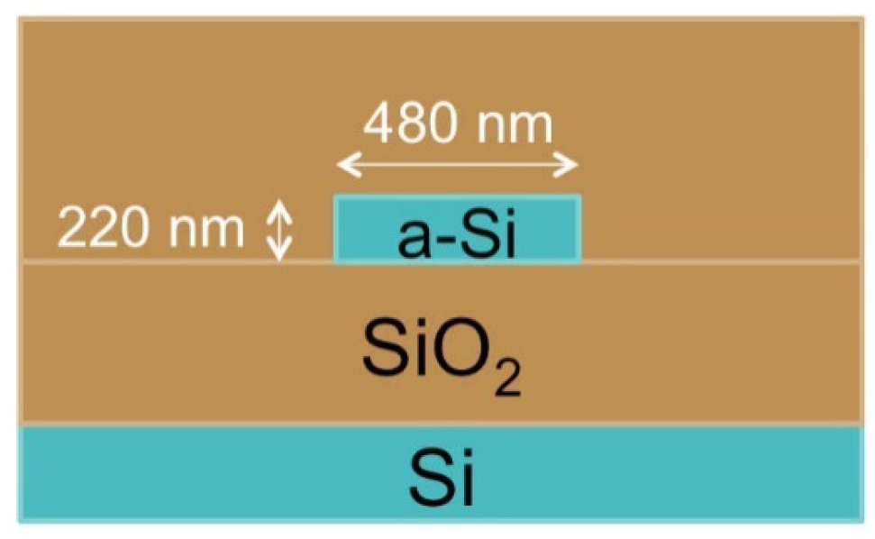
4.1. Engineered Silicon Rich Silicon Nitride
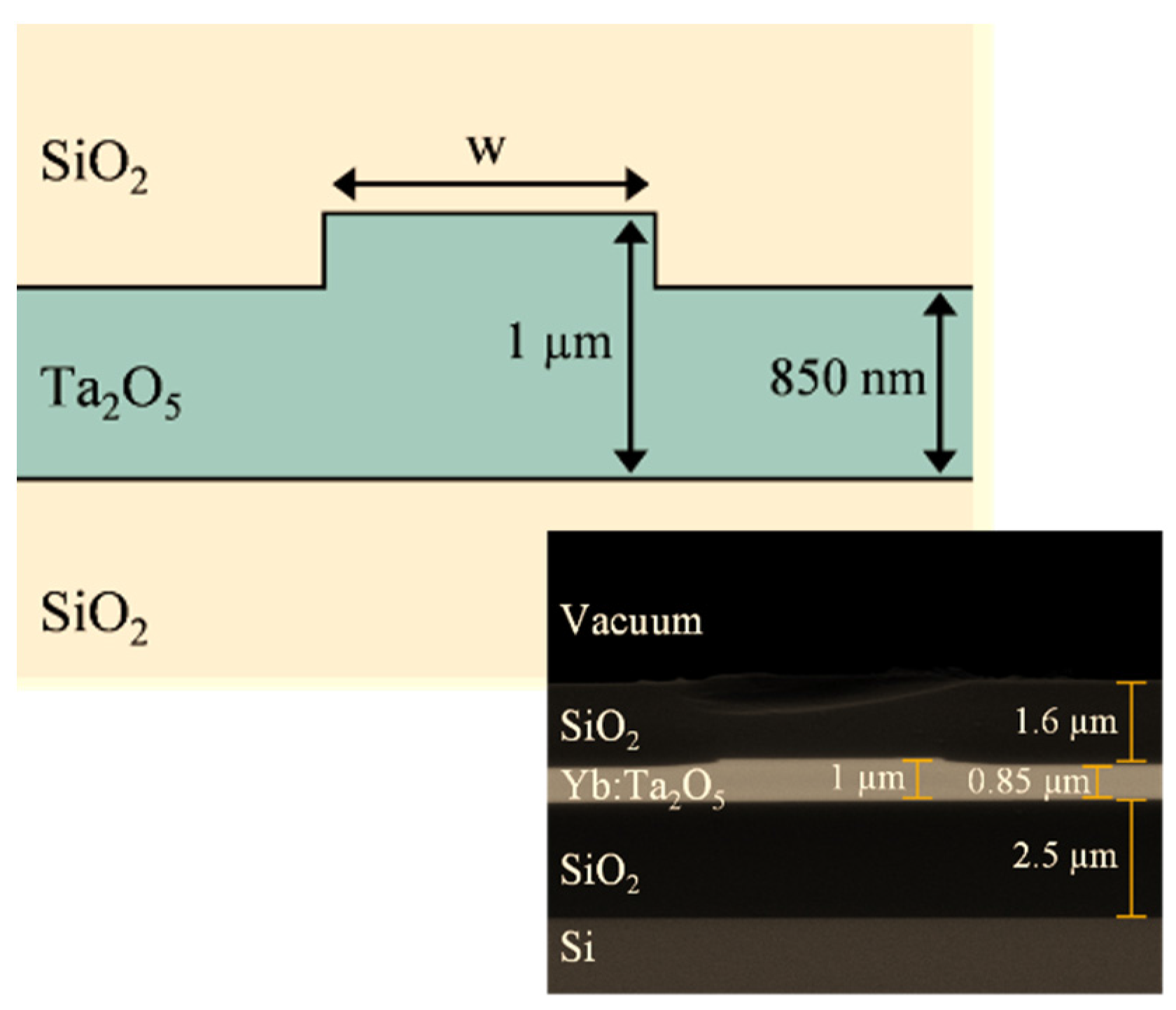
4.2. CMOS Compatible Tantalum Pentoxide Waveguides for Nonlinear Optical Processing
5. Conclusions
Acknowledgments
Author Contributions
Conflicts of Interest
References
- Doerr, C.R. Silicon photonic integration in telecommunications. Front. Phys. 2015, 3, 1–16. [Google Scholar] [CrossRef]
- Jalali, B.; Fathpour, S.; Reed, G.T. Silicon photonics. IEEE Microw. Mag. 2006, 24, 58–68. [Google Scholar] [CrossRef]
- Leuthold, J.; Koos, C.; Freude, W. Nonlinear silicon photonics. Nat. Photonics 2010, 4, 535–544. [Google Scholar] [CrossRef]
- Dinu, M.; Quochi, F.; Garcia, H. Third-order nonlinearities in silicon at telecom wavelengths. Appl. Phys. Lett. 2003, 82, 2954–2956. [Google Scholar] [CrossRef]
- Lin, Q.; Zhang, J.; Piredda, G.; Boyd, R.W.; Fauchet, P.M.; Agrawal, G.P. Dispersion of silicon nonlinearities in the near infrared region. Appl. Phys. Lett. 2007, 91, 1–4. [Google Scholar] [CrossRef]
- Vallaitis, T.; Bogatscher, S.; Alloatti, L.; Dumon, P.; Baets, R.; Scimeca, M.L.; Biaggio, I.; Diederich, F.; Koos, C.; Freude, W.; et al. Optical properties of highly nonlinear silicon-organic hybrid (SOH) waveguide geometries. Opt. Express 2009, 17, 17357–17368. [Google Scholar] [CrossRef] [PubMed]
- Rong, H.; Kuo, Y.-H.Y.; Liu, A.; Paniccia, M.; Cohen, O. High efficiency wavelength conversion of 10 Gb/s data in silicon waveguides. Opt. Express 2006, 14, 1182–1188. [Google Scholar] [CrossRef]
- Lee, B.; Biberman, A. Demonstration of broadband wavelength conversion at 40 Gb/s in silicon waveguides. Photonics Technol. Lett. 2009, 21, 182–184. [Google Scholar] [CrossRef]
- Hu, H.; Ji, H.; Galili, M.; Pu, M.; Peucheret, C.; Christian H Mulvad, H.; Yvind, K.; Hvam, J.M.; Jeppesen, P.; Oxenløwe, L.K. Ultra-high-speed wavelength conversion in a silicon photonic chip. Opt. Express 2011, 19, 19886–19894. [Google Scholar] [CrossRef] [PubMed]
- Lacava, C.; Strain, M.J.; Minzioni, P.; Cristiani, I.; Sorel, M. Integrated nonlinear Mach Zehnder for 40 Gbit/s all-optical switching. Opt. Express 2013, 21, 21587–21595. [Google Scholar] [CrossRef] [PubMed]
- Glesk, I.; Bock, P.J.; Cheben, P.; Schmid, J.H.; Lapointe, J.; Janz, S. All-optical switching using nonlinear subwavelength Mach-Zehnder on silicon. Opt. Express 2011, 19, 14031–14039. [Google Scholar] [CrossRef] [PubMed]
- Astar, W.; Driscoll, J.; Liu, X.; Dadap, J. Conversion of 10 Gb/s NRZ-OOK to RZ-OOK utilizing XPM in a Si nanowire. Opt. Express 2009, 17, 12987–12999. [Google Scholar] [CrossRef] [PubMed]
- Lu, Y.; Liu, F.; Qiu, M.; Su, Y. All-optical format conversions from NRZ to BPSK and QPSK based on nonlinear responses in silicon microring resonators. Opt. Express 2007, 15, 14275–14282. [Google Scholar] [CrossRef] [PubMed]
- Li, F.; Vo, T.D.; Husko, C.; Pelusi, M.; Xu, D.X.; Densmore, A.; Ma, R.; Janz, S.; Eggleton, B.J.; Moss, D.J. All-optical XOR logic gate for 40 Gb/s DPSK signals via FWM in a silicon nanowire. In Proceedings of 24th Annual of the IEEE Photonic Society, Crystal Gateway Marriott, Arlington, VA, USA, 9–13 October 2011; Volume 19, pp. 593–594.
- Vallaitis, T.; Hillerkuss, D.; Li, J.; Bonk, R.; Lindenmann, N.; Dumon, P.; Baets, R.; Scimeca, M.L.; Biaggio, I.; Diederich, F.; et al. All-Optical Wavelength Conversion Using Cross-Phase Modulation at 42.7 Gbit/s in Silicon-Organic Hybrid (SOH) Waveguides. In Proceedings of PS’09 International Conference on Photonics in Switching, Pisa, Italy, 15–19 September 2009; pp. 2–3.
- Martínez, A.; Blasco, J.; Sanchis, P.; Galán, J.V.; García-Rupérez, J.; Jordana, E.; Gautier, P.; Lebour, Y.; Hernández, S.; Guider, R.; et al. Ultrafast all-optical switching in a silicon-nanocrystal-based silicon slot waveguide at telecom wavelengths. Nano Lett. 2010, 10, 1506–1511. [Google Scholar] [CrossRef] [PubMed]
- Winzer, P.; Essiambre, R. Advanced Modulation Formats for High Capacity Optical Transport Network. J. Light. Technol. 2010, 24, 4711–4728. [Google Scholar] [CrossRef]
- Adams, R.; Spasojevic, M.; Chagnon, M.; Malekiha, M.; Li, J.; Plant, D.V.; Chen, L.R. Wavelength conversion of 28 GBaud 16-QAM signals based on four-wave mixing in a silicon nanowire. Opt. Express 2014, 22, 4083–4090. [Google Scholar] [CrossRef] [PubMed]
- Da Ros, F.; Vukovic, D.; Gajda, A.; Dalgaard, K.; Zimmermann, L.; Tillack, B.; Galili, M.; Petermann, K.; Peucheret, C. Phase regeneration of DPSK signals in a silicon waveguide with reverse-biased p-i-n junction. Opt. Express 2014, 22, 5029–5036. [Google Scholar] [CrossRef] [PubMed]
- Dolgaleva, K.; Ng, W.; Qian, L.; Aitchison, J. Compact highly-nonlinear AlGaAs waveguides for efficient wavelength conversion. Opt. Express 2011, 19, 1496–1498. [Google Scholar] [CrossRef] [PubMed]
- Lacava, C.; Pusino, V.; Minzioni, P.; Sorel, M.; Cristiani, I. Nonlinear properties of AlGaAs waveguides in continuous wave operation regime. Opt. Express 2014, 22, 5291–5298. [Google Scholar] [CrossRef] [PubMed]
- Eggleton, B.J.; Luther-Davies, B.; Richardson, K. Chalcogenide photonics. Nat. Photonics 2011, 5, 141–148. [Google Scholar]
- Ahmad, R.; Rochette, M. High efficiency and ultra broadband optical parametric four-wave mixing in chalcogenide-PMMA hybrid microwires. Opt. Express 2012, 20, 9572–9580. [Google Scholar] [CrossRef] [PubMed]
- Moss, D.J.; Morandotti, R.; Gaeta, A.L.; Lipson, M. New CMOS-compatible platforms based on silicon nitride and Hydex for nonlinear optics. Nat. Photonics 2013, 7, 597–607. [Google Scholar] [CrossRef]
- Koos, C.; Vorreau, P.; Vallaitis, T.; Dumon, P. All-optical high-speed signal processing with silicon – organic hybrid slot waveguides. Nat. Photonics 2009, 3, 1–4. [Google Scholar] [CrossRef]
- Lacava, C.; Ettabib, M.; Cristiani, I.; Fedeli, J.; Richardson, D.; Petropoulos, P. Ultra-Compact Amorphous Silicon Waveguide for Wavelength Conversion. IEEE Photonics Technol. Lett. 2016, 28, 410–414. [Google Scholar] [CrossRef]
- Ettabib, M.A.; Kapsalis, A.; Bogris, A.; Parmigiani, F.; Rancano, V.J.F.; Bottrill, K.; Brun, M.; Labeye, P.; Nicoletti, S.; Hammani, K.; et al. Polarization Insensitive Wavelength Conversion in a Low-Birefringence SiGe Waveguide. IEEE Photonics Technol. Lett. 2016, 28, 1221–1224. [Google Scholar] [CrossRef]
- Lacava, C.; Minzioni, P.; Baldini, E.; Tartara, L.; Fedeli, J.M.; Cristiani, I. Nonlinear characterization of hydrogenated amorphous silicon waveguides and analysis of carrier dynamics. Appl. Phys. Lett. 2013, 103. [Google Scholar] [CrossRef]
- Ettabib, M.A.; Parmigiani, F.; Kapsalis, A.; Bogris, A.; Brun, M.; Labeye, P.; Nicoletti, S.; Hammani, K. Record Phase Sensitive Extinction Ratio in a Silicon Germanium Waveguide. In Proceedings of the Lasers and Electro-Optics (CLEO 2015), San Jose, CA, USA, 10–15 May 2015.
- Ettabib, M.A.; Bottrill, K.; Parmigiani, F.; Kapsalis, A.; Bogris, A.; Brun, M.; Labeye, P.; Nicoletti, S.; Hammani, K.; Syvridis, D. All-optical Phase Regeneration with Record PSA Extinction Ratio in a Low-birefringence Silicon Germanium Waveguide. J. Light. Technol. 2016, 34, 3993–3998. [Google Scholar] [CrossRef]
- Ettabib, M.A.; Xu, L.; Bogris, A.; Kapsalis, A.; Belal, M.; Lorent, E.; Labeye, P.; Nicoletti, S.; Hammani, K.; Syvridis, D.; et al. Broadband telecom to mid-infrared supercontinuum generation in a dispersion- engineered silicon germanium waveguide. Opt. Lett. 2015, 40, 4118–4121. [Google Scholar] [CrossRef] [PubMed]
- Grillet, C.; Carletti, L.; Monat, C.; Grosse, P.; Ben Bakir, B.; Menezo, S.; Fedeli, J.M.; Moss, D.J. Amorphous silicon nanowires combining high nonlinearity, FOM and optical stability. Opt. Express 2012, 20, 22609–22615. [Google Scholar] [CrossRef] [PubMed]
- Suda, S.; Tanizawa, K.; Sakakibara, Y.; Kamei, T.; Nakanishi, K.; Itoga, E.; Ogasawara, T.; Takei, R.; Kawashima, H.; Namiki, S.; et al. Pattern-effect-free all-optical wavelength conversion using a hydrogenated amorphous silicon waveguide with ultra-fast carrier decay. Opt. Lett. 2012, 37, 1382–1384. [Google Scholar] [CrossRef] [PubMed]
- Narayanan, K.; Elshaari, A.W.; Preble, S.F. Broadband all-optical modulation in hydrogenated-amorphous silicon waveguides. Opt. Express 2010, 18, 9809–9814. [Google Scholar] [CrossRef] [PubMed]
- Matres, J.; Ballesteros, G.C.; Gautier, P.; Fédéli, J.-M.; Martí, J.; Oton, C.J. High nonlinear figure-of-merit amorphous silicon waveguides. Opt. Express 2013, 21, 3932–3940. [Google Scholar] [CrossRef] [PubMed]
- Kuyken, B.; Clemmen, S.; Selvaraja, S.K.; Bogaerts, W.; Van Thourhout, D.; Emplit, P.; Massar, S.; Roelkens, G.; Baets, R. On-chip parametric amplification with 26.5 dB gain at telecommunication wavelengths using CMOS-compatible hydrogenated amorphous silicon waveguides. Opt. Lett. 2011, 36, 552–554. [Google Scholar] [CrossRef] [PubMed]
- Mehta, P.; Healy, N.; Day, T.D.; Badding, J.V.; Peacock, A.C. Ultrafast wavelength conversion via cross-phase modulation in hydrogenated amorphous silicon optical fibers. Opt. Express 2012, 20, 26110–26116. [Google Scholar] [CrossRef] [PubMed]
- Kuyken, B.; Ji, H.; Clemmen, S.; Selvaraja, S.K.; Hu, H.; Pu, M.; Galili, M.; Jeppesen, P.; Morthier, G.; Massar, S.; et al. Nonlinear properties of and nonlinear processing in hydrogenated amorphous silicon waveguides. Opt. Express 2011, 19, B146–B153. [Google Scholar] [CrossRef] [PubMed]
- Taillaert, D.; Bienstman, P.; Baets, R. Compact efficient broadband grating coupler for silicon-on-insulator waveguides. Opt. Lett. 2004, 29, 2749–2751. [Google Scholar] [CrossRef] [PubMed]
- Agrawal, G.P. Nonlinear Fiber Optics, 5th ed.; Elsevier, Ed.; Academic Press: New York, NY, USA, 2013. [Google Scholar]
- Tsang, H.K.; Liu, Y. Nonlinear optical properties of silicon waveguides. Semicond. Sci. Technol. 2008, 23. [Google Scholar] [CrossRef]
- Lin, Q.; Painter, O.J.; Agrawal, G.P. Nonlinear optical phenomena in silicon waveguides: Modeling and applications. Opt. Express 2007, 15, 16604–16644. [Google Scholar] [CrossRef] [PubMed]
- Wang, K.-Y.; Foster, A.C. Ultralow power continuous-wave frequency conversion in hydrogenated amorphous silicon waveguides. Opt. Lett. 2012, 37, 1331–1333. [Google Scholar] [CrossRef] [PubMed]
- Shen, L.; Healy, N.; Mehta, P.; Day, T.D.; Sparks, J.R.; Badding, J.V.; Peacock, A.C. Nonlinear transmission properties of hydrogenated amorphous silicon core fibers towards the mid-infrared regime. Opt. Express 2013, 21, 13075–13083. [Google Scholar] [CrossRef] [PubMed]
- Narayanan, K.; Preble, S.F. Optical nonlinearities in hydrogenated-amorphous silicon waveguides. Opt. Express 2010, 18, 8998–9005. [Google Scholar] [CrossRef] [PubMed]
- Chagnon, M.; Spasojevic, M.; Adams, R.; Li, J.; Plant, D.V.; Chen, L.R. Wavelength Multicasting at 22-GBaud 16-QAM in a Silicon Nanowire Using Four-Wave Mixing. IEEE Photonics Technol. Lett. 2015, 27, 860–863. [Google Scholar] [CrossRef]
- Ros, F.D.; Yankov, M.P.; Silva, E.P.; Pu, M.; Ottaviano, L.; Hu, H. Characterization of a Wavelength Converter for 256-QAM Signals Based on an AlGaAs-On-Insulator. Nano-Waveguide 2016, 1, 662–664. [Google Scholar]
- Filion, B.; Ng, W.C.; Nguyen, A.T.; Rusch, L.A.; Larochelle, S. Wideband wavelength conversion of 16 Gbaud 16-QAM and 5 Gbaud 64-QAM signals in a semiconductor optical amplifier. Opt. Express 2013, 21, 19825–19833. [Google Scholar] [CrossRef] [PubMed]
- Paul, D.J. Si/SiGe heterostructures: From material and physics to devices and circuits. Semicond. Sci. Technol. 2004, 19, R75–R108. [Google Scholar] [CrossRef]
- Roth, J.E.; Fidaner, O.; Schaevitz, R.K.; Kuo, Y.-H.; Kamins, T.I.; Harris, J.S.; Miller, D.A.B. Optical modulator on silicon employing germanium quantum wells. Opt. Express 2007, 15, 5851–5859. [Google Scholar] [CrossRef] [PubMed]
- Tsybeskov, L.; Lockwood, D.J. Silicon-germanium nanostructures for light emitters and on-chip optical interconnects. Proc. IEEE 2009, 97, 1284–1303. [Google Scholar] [CrossRef]
- Chen, L.; Lipson, M. Ultra-low capacitance and high speed germanium photodetectors on silicon. Opt. Express 2009, 17, 7901–7906. [Google Scholar] [CrossRef] [PubMed]
- Vivien, L.; Polzer, A.; Marris-Morini, D.; Osmond, J.; Hartmann, J.M.; Crozat, P.; Cassan, E.; Kopp, C.; Zimmermann, H.; Fédéli, J.M. Zero-bias 40 Gbit/s germanium waveguide photodetector on silicon. Opt. Express 2012, 20, 1096–1101. [Google Scholar] [CrossRef] [PubMed]
- Ettabib, M.A.; Hammani, K.; Parmigiani, F.; Jones, L.; Kapsalis, A.; Bogris, A.; Syvridis, D.; Brun, M.; Labeye, P.; Nicoletti, S.; et al. FWM-based wavelength conversion of 40 Gbaud PSK signals in a silicon germanium waveguide. Opt. Express 2013, 21, 17–23. [Google Scholar] [CrossRef] [PubMed]
- Hammani, K.; Ettabib, M.A.; Bogris, A.; Kapsalis, A.; Syvridis, D.; Brun, M.; Labeye, P.; Nicoletti, S.; Richardson, D.J.; Petropoulos, P. Optical properties of silicon germanium waveguides at telecommunication wavelengths. Opt. Express 2013, 21, 16690–16701. [Google Scholar] [CrossRef] [PubMed]
- Tittelbach, G.; Richter, B.; Karthe, W. Comparison of three transmission methods for integrated optical waveguide propagation loss measurement. Pure Appl. Opt. 1993, 2, 683–706. [Google Scholar] [CrossRef]
- Ettabib, M.; Lacava, C.; Liu, Z.; Bogris, A.; Kapsalis, A.; Brun, M.; Labeye, P.; Nicoletti, S.; Syvridis, D.; Richardson, D.J.; et al. Wavelength Conversion of 16-QAM and 64-QAM Signals in a Compact SiGe Waveguide. Manuscr. Submitt. Publ. 2016, in press. [Google Scholar]
- Ros, F.D.; Porto, E.; Zibar, D.; Chu, S.T.; Little, B.E.; Morandotti, R.; Galili, M.; Moss, D.J.; Oxenløwe, L.K. Low-penalty up to 16-QAM wavelength conversion in a low loss CMOS compatible spiral waveguide. In Proceedings of the Optical Fiber Communication Conference, Anaheim, CA, USA, 20–24 March 2016.
- Xing, L.; Pu, M.; Zhou, B.; Clemens, K.; Attila, F.; Torres-Company, V.; Bache, M. Octave-spanning supercontinuum generation in a silicon-rich nitride waveguide. Opt. Lett. 2016, 41, 2719–2722. [Google Scholar]
- Krückel, C.J.; Torres-Company, V.; Andrekson, P.A.; Spencer, D.T.; Bauters, J.F.; Heck, M.J.R.; Bowers, J.E. Continuous wave-pumped wavelength conversion in low-loss silicon nitride waveguides. Opt. Lett. 2015, 40, 875–878. [Google Scholar] [CrossRef] [PubMed]
- Baets, R.; Subramanian, A.Z.; Clemmen, S.; Kuyken, B.; Bienstman, P.; Nicolas, T.L.; Roelkens, G.; Van Thourhout, D.; Hein, P.; Severi, S. Silicon Photonics: Silicon nitride versus silicon-on-insulator. In Proceedings of the Optical Fiber Communication Conference, Anaheim, CA, USA, 20–24 March 2016.
- Bauters, J.F.; Heck, M.J.R.; John, D.; Dai, D.; Tien, M.-C.; Barton, J.S.; Leinse, A.; Heideman, R.G.; Blumenthal, D.J.; Bowers, J.E. Ultra-low-loss high-aspect-ratio Si3N4 waveguides. Opt. Express 2011, 19, 3163–3174. [Google Scholar] [CrossRef] [PubMed]
- Levy, J.; Foster, M.; Gaeta, A.L.; Lipson, M. Harmonic generation in silicon nitride ring resonators. Opt. Express 2011, 19, 11415–11421. [Google Scholar] [CrossRef] [PubMed]
- Tien, M.-C.; Bauters, J.F.; Heck, M.J.R.; Blumenthal, D.J.; Bowers, J.E. Ultra-low loss Si3N4 waveguides with low nonlinearity and high power handling capability. Opt. Express 2010, 18, 23562–23568. [Google Scholar] [CrossRef] [PubMed]
- Choi, J.W.; Chen, G.F.R.; Ng, D.K.T.; Ooi, K.J.A.; Tan, D.T.H. Wideband nonlinear spectral broadening in ultra-short ultra—silicon rich nitride waveguides. Sci. Rep. 2016, 1–8. [Google Scholar] [CrossRef] [PubMed]
- Krückel, C.J.; Fülöp, A.; Klintberg, T.; Bengtsson, J.; Andrekson, P.A.; Torres-Company, V. Linear and nonlinear characterization of low-stress high-confinement silicon-rich nitride waveguides. Opt. Express 2015, 23, 25827–25837. [Google Scholar] [CrossRef] [PubMed]
- Wang, T.; Ng, D.K.T.; Ng, S.; Toh, Y.; Chee, A.K.L.; Chen, G.F.R.; Wang, Q.; Tan, D.T.H. Supercontinuum generation in bandgap engineered, back-end CMOS compatible silicon rich nitride waveguides. Laser Photonics Rev. 2015, 9, 498–506. [Google Scholar] [CrossRef]
- Lacava, C.; Stankovic, S.; Khokhar, A.Z.; Bucio, T.D.; Gardes, F.Y.; Richardson, D.J.; Reed, G.T. CMOS-compatible Silicon-Rich Nitride Waveguides for Ultrafast Nonlinear Signal Processing. In Proceedings of the Conference on Lasers and Electro-Optics, San Jose, CA, USA, 5–10 June 2016.
- Lacava, C.; Stankovic, S.; Khokhar, A.Z.; Bucio, T.D.; Gardes, F.; Reed, G.T.; Richardson, D.J.; Petropoulos, P. Si-rich Silicon Nitride for Nonlinear Signal Processing Applications. Sci. Rep. Nat. Publ. Group 2016, in press. [Google Scholar]
- Tai, C.-Y.; Wilkinson, J.S.; Perney, N.M.B.; Netti, M.C.; Cattaneo, F.; Finlayson, C.E.; Baumberg, J.J. Determination of nonlinear refractive index in a Ta2O5 rib waveguide using self-phase modulation. Opt. Express 2004, 12, 5110–5116. [Google Scholar] [CrossRef] [PubMed]
- Lacava, C.; Aghajani, A.; Hua, P.; Richardson, D.J.; Petropoulos, P.; Wilkinson, J.S. Nonlinear optical properties of ytterbium-doped tantalum pentoxide rib waveguides on silicon at telecom wavelengths. In Proceedings of the Optical Fiber Communication Conference, Anaheim, CA, USA, 20–24 March 2016.
- Wu, C.-L.; Chiu, Y.-J.; Chen, C.-L.; Lin, Y.-Y.; Chu, A.-K.; Lee, C.-K. Four-wave-mixing in the loss low submicrometer Ta2O5 channel waveguide. Opt. Lett. 2015, 40, 4528–4531. [Google Scholar] [CrossRef] [PubMed]
- Aghajani, A.; Murugan, G.S.; Sessions, N.P.; Apostolopoulos, V.; Wilkinson, J.S. Waveguide lasers in ytterbium-doped tantalum pentoxide on silicon. Opt. Lett. 2015, 40, 2549–2552. [Google Scholar] [CrossRef] [PubMed]


| α0 (dB/cm) | Re{γ} (Wm)−1 | Im{γ} (Wm)−1 | Free Carrier (FC) Recovery Time (ns) | αFC (cm2) |
|---|---|---|---|---|
| 4.7 | 800 ± 50 | 15.5 ± 2 | 1.87 | 0.8 × 10⁻¹⁷ |
| Reference | Re{γ} (Wm)−1 | Im{γ} (Wm)−1 | FOM (Figure Of Merit) |
|---|---|---|---|
| [26] | 800 | 15 | 4.7 |
| [35] | 332 | 5.43 | 4.9 |
| [32] | 1200 | 12.5 | 7.6 |
| [36] | 770 | 19.6 | 3.12 |
| [45] | 2003 | 205 | 0.85 |
| Ge Concentration/Waveguide Width | 0.3 µm | 0.6 µm | 0.8 µm | 1 µm | 1.5 µm | 2 µm |
|---|---|---|---|---|---|---|
| x = 0.1 | High loss (> 5 dB/cm) | 4.75 dB/cm | 0.43 dB/cm | 0.65 dB/cm | ||
| x = 0.2 | 3.90 dB/cm | 2.38 dB/cm | 2.38 dB/cm | 1.40 dB/cm | 1.52 dB/cm | 2.60 dB/cm |
| x = 0.3 | 3.47 dB/cm | 4.56 dB/cm | 4.77 dB/cm | 5.21 dB/cm | 4.77 dB/cm | 4.34 dB/cm |
| Re{γ} (Wm)−1 | Im{γ} (Wm)−1 | FOM | |
|---|---|---|---|
| W = 1000 nm, Ge (10%) | 16 | 0.76 | 1.67 |
| W = 1000 nm, Ge (20%) | 25 | 1.16 | 1.71 |
| W = 1000 nm, Ge (30%) | 35 | 1.98 | 1.40 |
| Device | Signal Type | Conversion Efficiency (dB) | 3 dB Conversion Bandwidth (nm) | OSNR 1 Penalty | CMOS 1 Compatible |
|---|---|---|---|---|---|
| a-Si (this work reported in [26]) | 10 Gbaud DPSK 1 | −26 dB | ~25 nm | <1 dB | Yes |
| Si-Ge (this work reported in [57]) | 10 Gbaud 64 QAM 1 | −9.7 dB | ~30 nm | <1 dB | Yes |
| c-Si [18] | 28 Gbaud 16 QAM | −17.5 dB | ~30 nm | 4 dB at BER 1 = 10−5 | Yes |
| AlGaAs on SOI [47] | 10 Gbaud 256 QAM | −13 dB | ~28 nm | 2.5 dB | No |
| Hydex [58] | 10 Gbaud 16 QAM | −40 dB | ~10 nm | 0.5 dB | Yes |
| Material Refractive Index | α0 (dB/cm) | Re{γ} (Wm)−1 | Im{γ} (Wm)−1 | |
|---|---|---|---|---|
| Wafer_01 | 2.01 | 1.38 | 1.54 | Negligible |
| Wafer_02 | 2.49 | 1.5 | 16 | Negligible |
| Wafer_03 | 2.79 | 5.5 | 28 | 2.58 |
© 2017 by the authors; licensee MDPI, Basel, Switzerland. This article is an open access article distributed under the terms and conditions of the Creative Commons Attribution (CC BY) license (http://creativecommons.org/licenses/by/4.0/).
Share and Cite
Lacava, C.; Ettabib, M.A.; Petropoulos, P. Nonlinear Silicon Photonic Signal Processing Devices for Future Optical Networks. Appl. Sci. 2017, 7, 103. https://doi.org/10.3390/app7010103
Lacava C, Ettabib MA, Petropoulos P. Nonlinear Silicon Photonic Signal Processing Devices for Future Optical Networks. Applied Sciences. 2017; 7(1):103. https://doi.org/10.3390/app7010103
Chicago/Turabian StyleLacava, Cosimo, Mohamed A. Ettabib, and Periklis Petropoulos. 2017. "Nonlinear Silicon Photonic Signal Processing Devices for Future Optical Networks" Applied Sciences 7, no. 1: 103. https://doi.org/10.3390/app7010103
APA StyleLacava, C., Ettabib, M. A., & Petropoulos, P. (2017). Nonlinear Silicon Photonic Signal Processing Devices for Future Optical Networks. Applied Sciences, 7(1), 103. https://doi.org/10.3390/app7010103