
Analysis of Losses in Open Circuit Voltage for an 18-μm Silicon Solar Cell

Abstract
:1. Introduction

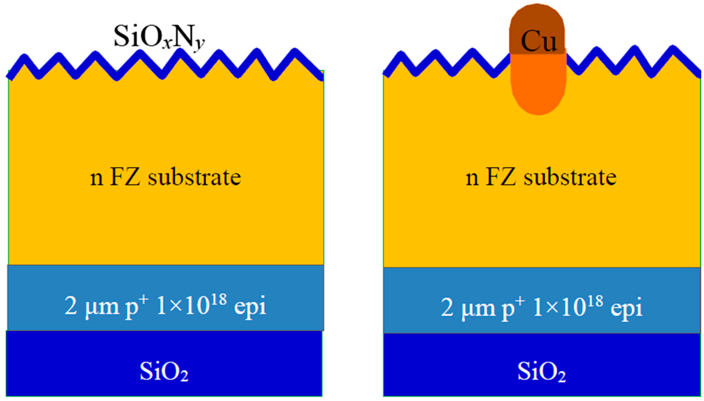
2. Fabrication
3. Voc Losses Analysis
3.1. Voc in Ideal Case

| Steps | J0 Components | J0 Value (A/cm2) | Voc (mV) |
|---|---|---|---|
| -- | J0b | 4.73 × 10⁻¹⁵ | -- |
| -- | J0e | 3.03 × 10⁻¹⁷ | -- |
| 1 | J0b + J0e | 4.76 × 10⁻¹⁵ | 767.0 |
3.2. Voc Loss Due to Surface Recombination
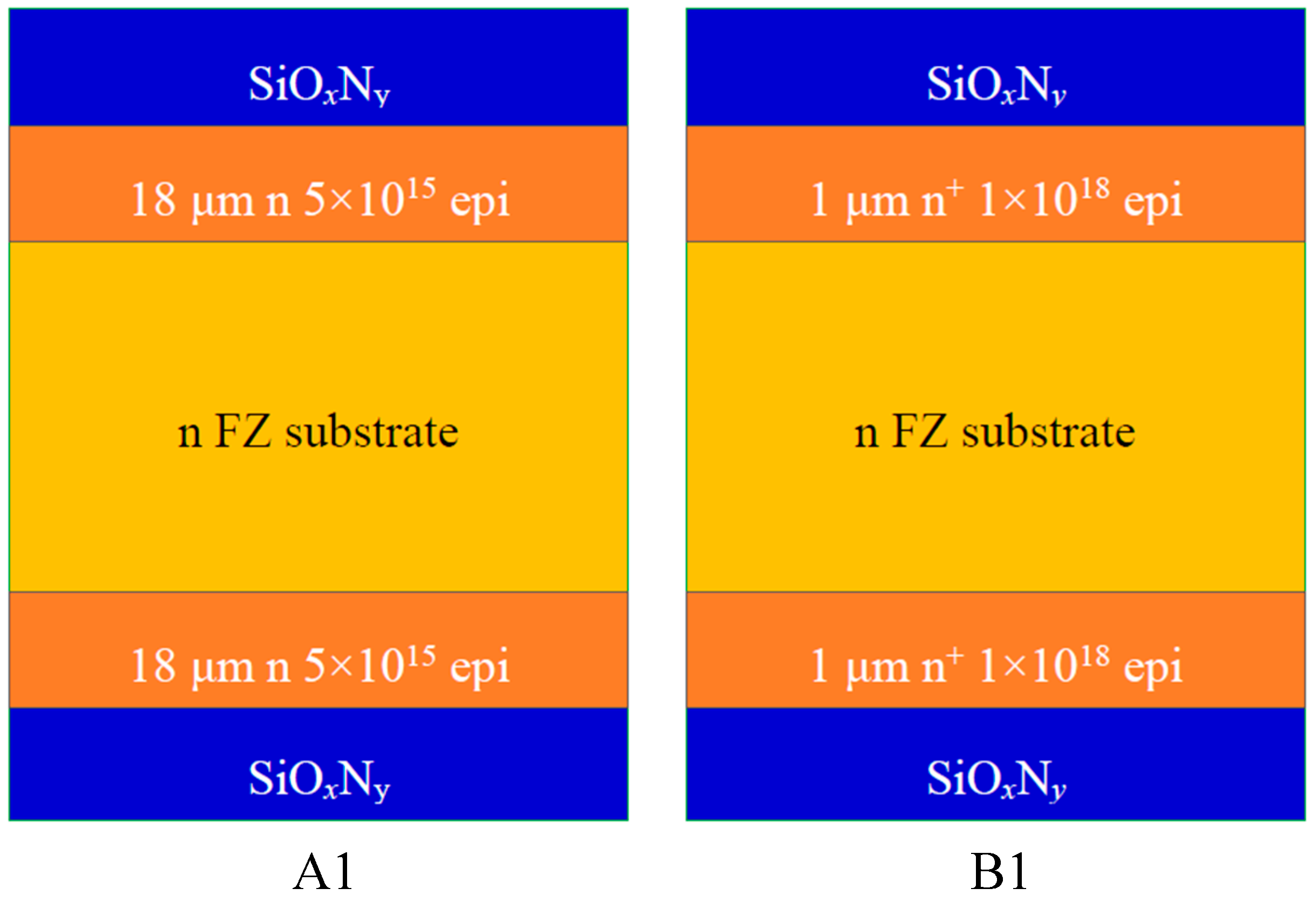
3.2.1 SRV on a Passivated n type Surface

| ID | iVoc (mV) | Lifetime (μs) | SRV (cm/s) |
|---|---|---|---|
| Group A1 | 718 | 1085 | 13 |
| Group B1 | 696 | 556 | 26 |
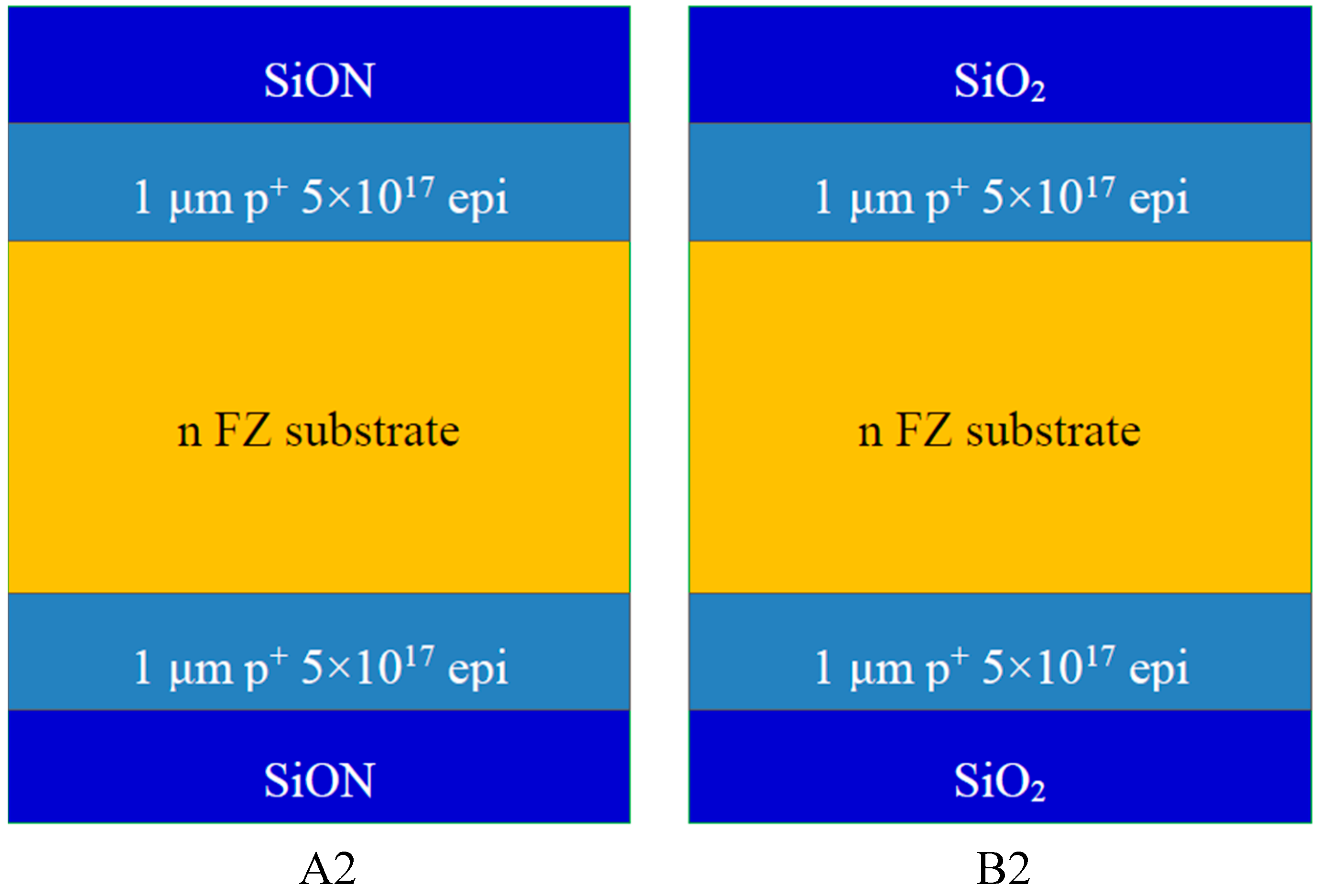
3.2.2. SRV on a Passivated p+ Surface

| Group | Lifetime (μs) | iVoc (mV) | J0e (A/cm2) | SRV (cm/s) |
|---|---|---|---|---|
| A2 | 161–221 | 644–658 | -- | -- |
| B2 | 139–157 | 637–642 | 1.85 × 10⁻¹³ ~ 2.0 × 10⁻¹³ | 1551–1677 |
3.3. Voc Losses Calculation
| Steps | Component | J0 (A/cm2) | Voc (mV) | Steps |
|---|---|---|---|---|
| 1 | J0b + J0e | 4.76 × 10⁻¹⁵ | 767.0 | Maximum |
| 2 | J0bs | 4.23 × 10⁻¹⁴ | >710.1 | Front SiOxNy |
| -- | J0es | 6.12 × 10⁻¹⁴ | -- | -- |
| 3 | J0bs + J0es | 1.04 × 10⁻¹³ | 687.0 | Front SiOxNy + Rear SiO2 |
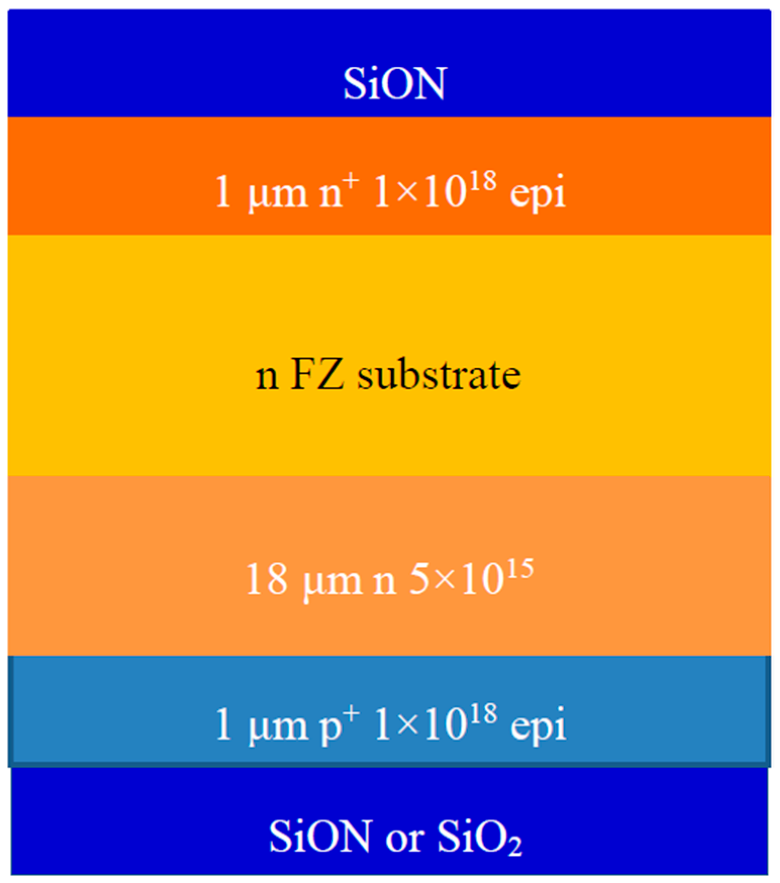
3.4. Measured Voc on Test Samples

| ID | Lifetime (μs) | iVoc (mV) |
|---|---|---|
| Test samples | 383–674 | 682–703 |
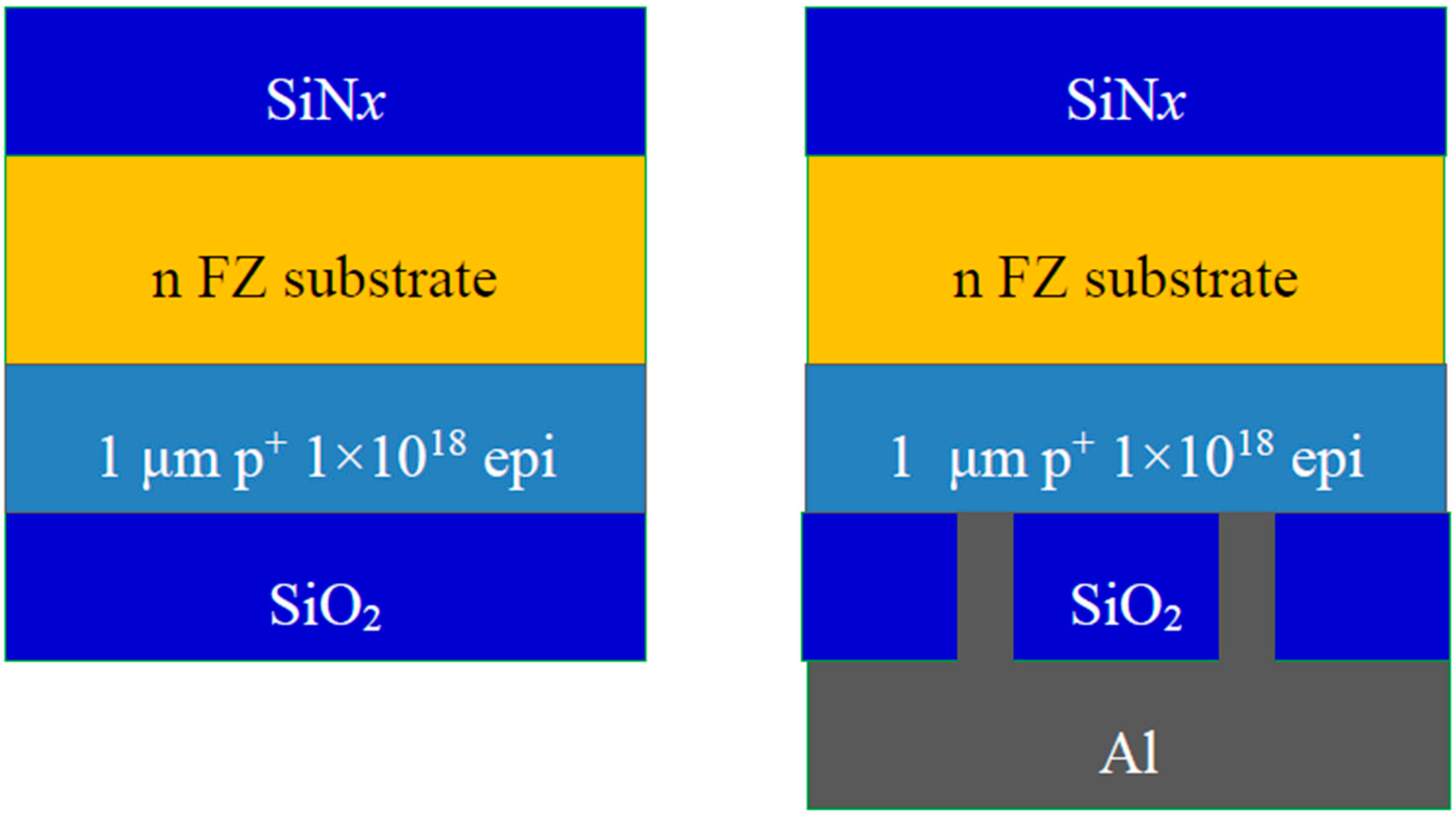
4. Voc Loss Due to Rear Surface Metallization
4.1. Voc Losses Calculation
| Steps | Component | J0 (A/cm2) | Voc (mV) | Steps |
|---|---|---|---|---|
| 3 | J0bs + J0es | 1.04 × 10⁻¹³ | 687.0 | Rear SiO2 |
| -- | J0e-pc | 9.76 × 10⁻¹⁴ | -- | -- |
| 4 | J0bs + J0es + J0e-pc | 2.02 × 10⁻¹³ | 670.0 | Rear contact |
4.2. Measured Voc on Test Samples

| Steps | Front SiOxNy/Rear SiO2 | Rear metallization | |
|---|---|---|---|
| Values | Lifetime (μs) | iVoc (mV) | Voc (mV) |
| 445.2 | 685.4 | 665–673 | |
5. Voc Loss Due to Front Surface Metallization
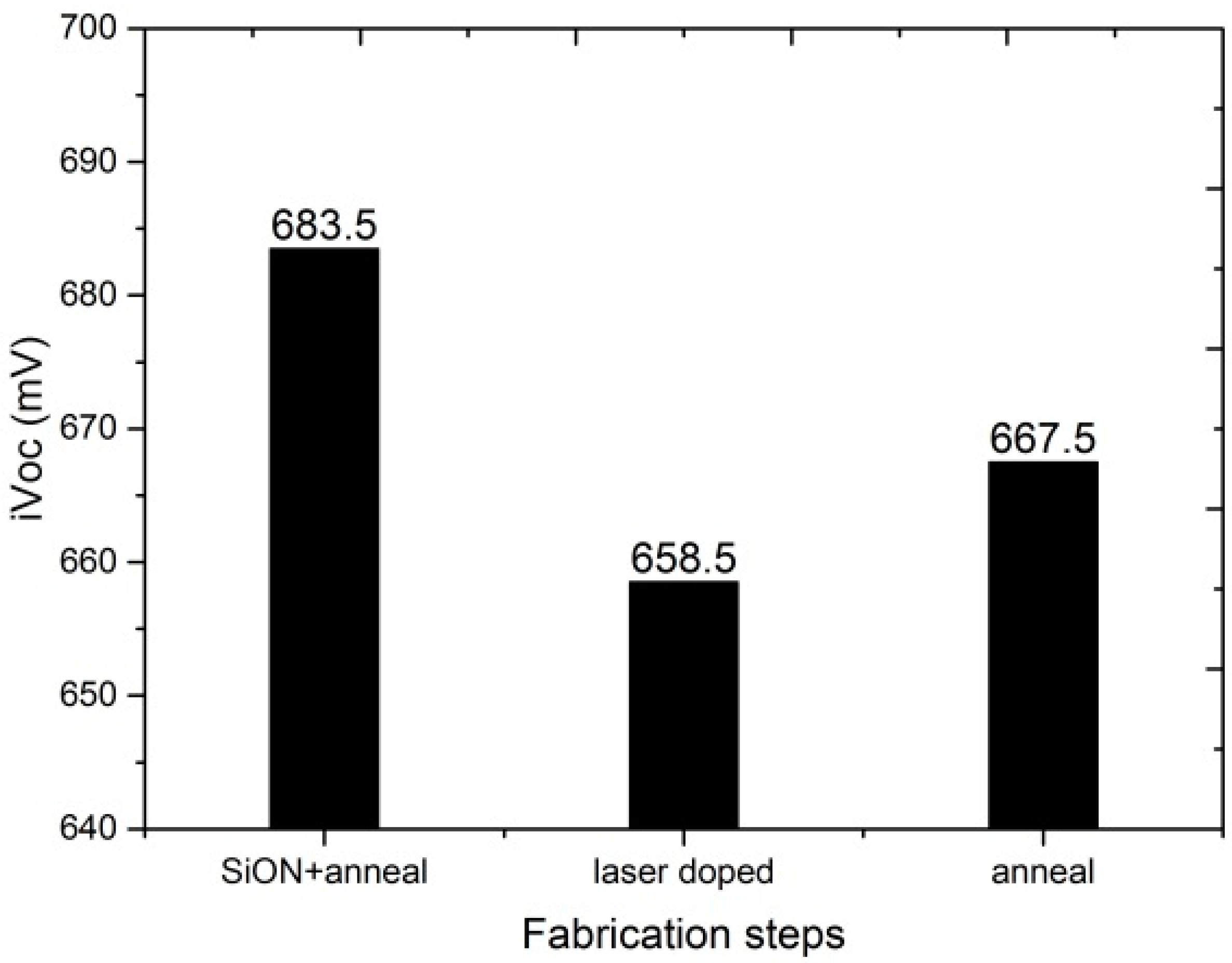
5.1. Laser Doping

5.2. Metallization
| Steps | Component | J0 (A/cm2) | Voc (mV) | Steps |
|---|---|---|---|---|
| 4 | J0bs + J0es + J0e-pc | 2.02 × 10⁻¹³ | 670.0 | Rear contact |
| -- | J0b-ld | 2.14 × 10⁻¹³ | -- | -- |
| 5 | J0bs + J0es + J0e-pc + J0b-ld | 4.16 × 10⁻¹³ | 650.0 | Laser doping/metallization |
6. Voc Loss Due to Edge Isolation
| Steps | Component | J0 (mA/cm2) | Voc (mV) | Steps |
|---|---|---|---|---|
| 5 | J0bs + J0es + J0e-pc + J0b-ld | 4.16 × 10⁻¹³ | 650.0 | Laser doping/metallization |
| -- | J0-edge | 1.93 × 10⁻¹³ | -- | -- |
| 6 | J0bs + J0es + J0e-pc + J0b-ld + J0-edge | 6.09 × 10⁻¹³ | 640.0 | Edge isolation |
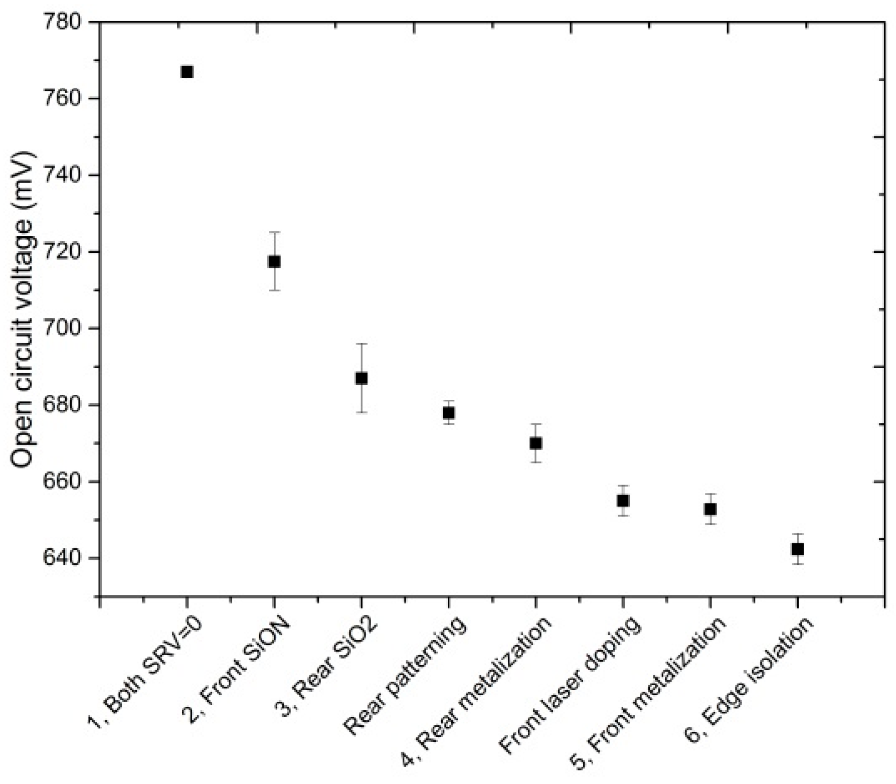
7. Summary of Voc Losses
Acknowledgment
Author Contributions
Conflicts of Interest
References
- Tiedje, T.; Yablonovitch, E.; Cody, G.D.; Brooks, B.G. Limiting efficiency of silicon solar cells. IEEE Trans. Electron Devices 1984, 31, 711–716. [Google Scholar] [CrossRef]
- Spitzer, M.; Shewchun, J.; Vera, E.; Loferski, J. Ultra high efficiency thin silicon p-n junction solar cells using reflecting surfaces. In Proceedings of the 14th Photovoltaic Specialists Conference, San Diego, CA, USA, 7–10 January 1980; pp. 375–380.
- Wolf, M. Updating the limit efficiency of silicon solar cells. IEEE Trans. Electron Devices 1980, 27, 751–760. [Google Scholar] [CrossRef]
- Swanson, R.M. Approaching the 29% limit efficiency of silicon solar cells. In Proceedings of the 2005 Conference Record of the Thirty-first IEEE Photovoltaic Specialists Conference, Lake Buena Vista, FL, USA, 3–7 January 2005; pp. 889–894.
- Wang, L.; Lochtefeld, A.; Han, J.; Gerger, A.P.; Carroll, M.; Ji, J.; Lennon, A.; Li, H.; Opila, R.; Barnett, A. Development of a 16.8% Efficient 18-μm Silicon Solar Cell on Steel. IEEE J. Photovol. 2014, 4, 1397–1404. [Google Scholar] [CrossRef]
- Wang, L.; Li, H.; Shen, C.; Han, J.; Teng, P.; Abbott, M.; Lochtefeld, A.; Opila, R.; Barnett, A. Photoluminescence analysis of a 16.8% efficient 18-um silicon solar cell. Int. J. Emerg. Technol. Adv. Eng. 2015, 5, 8–14. [Google Scholar]
- Clugston, D.A.; Basore, P.A. PC1D version 5: 32-bit solar cell modeling on personal computers. In Proceedings of the 1997 Conference Record of the Twenty-Sixth IEEE Photovoltaic Specialists Conference, Anaheim, CA, USA, 29 September–3 October 1997; pp. 207–210.
- Ai, B.; Zhang, Y.; Deng, Y.; Shen, H. Study on device simulation and performance optimization of the epitaxial crystalline silicon thin film solar cell. Sci. China Technol. Sci. 2012, 55, 3187–3199. [Google Scholar] [CrossRef]
- Hallam, B.; Tjahjono, B.; Wenham, S. Effect of PECVD silicon oxynitride film composition on the surface passivation of silicon wafers. Sol. Energy Mater. Sol. Cells 2012, 96, 173–179. [Google Scholar] [CrossRef]
- Sinton, R.A.; Cuevas, A. Contactless determination of current-voltage characteristics and minority—Carrier lifetimes in semiconductors from quasi-steady-state photoconductance data. Appl. Phys. Lett. 1996, 69, 2510–2512. [Google Scholar] [CrossRef]
- PV Lighthouse. Available online: http://www.pvlighthouse.com.au/calculators/calculators.aspx (accessed on 23 September 2015).
- King, R.R.; Swanson, R.M. Studies of diffused boron emitters: Saturation current, bandgap narrowing, and surface recombination velocity. IEEE Trans. Electron Devices 1991, 38, 1399–1409. [Google Scholar] [CrossRef]
- Altermatt, P.P.; Schenk, A.; Geelhaar, F.; Heiser, G. Reassessment of the intrinsic carrier density in crystalline silicon in view of band-gap narrowing. J. Appl. Phys. 2003, 93, 1598–1604. [Google Scholar] [CrossRef]
- Green, M.A.; Blakers, A.W.; Zhao, J.; Milne, A.M.; Wang, A.; Dai, X. Characterization of 23-percent efficient silicon solar cells. IEEE Trans. Electron Devices 1990, 37, 331–336. [Google Scholar] [CrossRef]
- Sabbah, A.; Riffe, D.M. Measurement of silicon surface recombination velocity using ultrafast pump-probe reflectivityin the near infrared. J. Appl. Phys. 2000, 88, 6954–6957. [Google Scholar] [CrossRef]
- Sugianto, A.; Bovatsek, J.; Wenham, S.; Tjahjono, B.; Xu, G.; Yao, Y.; Hallam, B.; Bai, X.; Kuepper, N.; Chong, C.M. 18.5% laser-doped solar cell on CZ p-type silicon. In Proceedings of the 2010 35th IEEE Photovoltaic Specialists Conference (PVSC), Honolulu, HI, USA, 20–25 June 2010; pp. 000689–000694.
- Hauser, A.; Hahn, G.; Spiegel, M.; Feist, H.; Breitenstein, O.; Rakotoniaina, J.; Fath, P.; Bucher, E. Comparison of different techniques for edge isolation. In Proceedings of the 17th European Photovoltaic Solar Energy Conference; McNelis, B., Palz, W., Ossenbrink, H.A., Eds.; WIP-ETA: Florence, Italy, 2001; pp. 1739–1742. [Google Scholar]
- Hamammu, I.; Ibrahim, K. Solar cell edge shunt isolation: A simplified approach. In Proceedings of IEEE International Conference on Semiconductor Electronics, Pulau Pinang, Malaysia, 19–21 December 2002; pp. 230–232.
© 2015 by the authors; licensee MDPI, Basel, Switzerland. This article is an open access article distributed under the terms and conditions of the Creative Commons Attribution license (http://creativecommons.org/licenses/by/4.0/).
Share and Cite
Wang, L.; Han, J.; Lochtefeld, A.; Gerger, A.; Barnett, A. Analysis of Losses in Open Circuit Voltage for an 18-μm Silicon Solar Cell. Appl. Sci. 2015, 5, 682-694. https://doi.org/10.3390/app5040682
Wang L, Han J, Lochtefeld A, Gerger A, Barnett A. Analysis of Losses in Open Circuit Voltage for an 18-μm Silicon Solar Cell. Applied Sciences. 2015; 5(4):682-694. https://doi.org/10.3390/app5040682
Chicago/Turabian StyleWang, Lu, Jianshu Han, Anthony Lochtefeld, Andrew Gerger, and Allen Barnett. 2015. "Analysis of Losses in Open Circuit Voltage for an 18-μm Silicon Solar Cell" Applied Sciences 5, no. 4: 682-694. https://doi.org/10.3390/app5040682
APA StyleWang, L., Han, J., Lochtefeld, A., Gerger, A., & Barnett, A. (2015). Analysis of Losses in Open Circuit Voltage for an 18-μm Silicon Solar Cell. Applied Sciences, 5(4), 682-694. https://doi.org/10.3390/app5040682