Article

A New Mechanism for THz Detection Based on the Tunneling Effect in Bi-Layer Graphene Nanoribbons

by
Antonio Maffucci
1,2
1
Department of Electrical and Information Engineering, University of Cassino and Southern Lazio, via G. Di Biasio 43, Cassino 03043, Italy
2
National Institute for Nuclear Physics, INFN, via E. Fermi 10, Frascati 00044, Italy
Appl. Sci. 2015, 5(4), 1102-1116; https://doi.org/10.3390/app5041102
Submission received: 14 October 2015 / Revised: 27 October 2015 / Accepted: 3 November 2015 / Published: 12 November 2015
(This article belongs to the Section Nanotechnology and Applied Nanosciences)

Abstract

:
A new possible mechanism of signal detection in the THz range is investigated, based on the excitation of resonances due to the tunneling effect between two graphene nanoribbons. A simple detector is proposed, where two graphene nanoribbons are used to contact two copper electrodes. The terminal voltages are shown to exhibit strong resonances when the frequency of an external impinging field is tuned to the characteristic tunneling frequency of the graphene layer pair. An electrodynamic model for the electron transport along the graphene nanoribbons is extended here to include the tunneling effect, and a coupled transmission line model is finally derived. This model is able to predict not only the tunneling resonance, but also the well-known plasmon resonances, related to the propagation of slow surface waves.

Graphical Abstract

1. Introduction

The terahertz range is a fascinating and promising frontier of research for a wide range of technological applications, from medical imaging to security, from astrophysics to consumer electronics [1,2,3]. The quickly increasing interest in THz range technology is driven by the possibility to fabricate reliable and portable coherent sources and sensitive detectors, in order to exploit the features of the field in such a range (0.1–10 THz), also known as the submillimeter wave range (1–0.03 mm).
The THz range has begun to be explored thoroughly only over the last decade given the difficulties to approach such a range, either by extending the paradigms of the RF/microwave technology (hence, coming from lower frequencies) or those of the infrared (IR), or far infrared (FIR) technology (hence, coming from higher frequencies), e.g, [4,5]. The THz range is, indeed, a sort of an unexplored “boundary” region between electronics and photonics, which was usually referred to as the “THz gap”, to underline the difficulty to access this range by using the classical electronics or photonics technologies. In fact, classical microwave devices exhibit a dramatic drop of performance for frequencies above 100 GHz, due to the degradation of the transport properties. In addition, classical photonics devices cannot be efficiently used for frequencies below 10 THz, due to the steep increase of the conversion of the photon energy to the thermal energy.
Using classical materials and classical design approaches it is extremely difficult to realize a compact THz circuit: it is indeed difficult to design lumped elements whose characteristic dimensions become comparable to, or higher than, the wavelength. For the same reason, the electrical interconnects no longer behave as transmission lines carrying only the fundamental mode, but rather as multimode channels, which makes frequency tuning difficult, limits the range of operating frequencies, and introduces high sensitivity to errors of their setting. Furthermore, low-loss, hollow, single-mode waveguides and resonators would require a costly surface purity. As a consequence, there is a lack of efficient sources of submillimeter-wave power sources, detectors, and low-loss interconnects in such a range, compared to the well-assessed RF/microwave or IR/FIR technology.
The recent advances in nanotechnology suggested an alternative route to the THz technology, based on fascinating mechanical, electronic, and optical properties of the different nano-materials proposed in the last decade. Single-mode components (photonic crystals, transmission lines, microcavities, antennas) and lumped elements (capacitors, inductors, resistors, interconnects) have been fabricated by means of nano-sized elements, exploiting their novel electromagnetic properties. In general, they are related to their discrete spectrum of energy states, which is a consequence of the spatial confinement of the charge carrier’s motion to sizes comparable with the de Broglie wavelength. These nanostructures are characterized by novel dispersion providing their unusual electromagnetic response.
Carbon-based materials, like carbon nanotubes (CNTs) or graphene nanoribbons (GNRs), are definitely the most promising nanostructured materials for realizing the building blocks of high-frequency devices [5,6,7], given their outstanding electrical, thermal, and mechanical properties [8,9,10], which make them of great interest for THz applications [11,12,13,14]. Indeed, carbon-based materials are proposed for several THz devices, like ballistic transistors [15], or waveguides and nanoantennas [16,17].
Carbon materials are suitable for realizing THz sources and emitters [18,19]. To this end, two main mechanisms have been proposed to excite resonances in the THz range. The most popular one is based on plasmon resonances. In fact, in the THz range the carbon nanotubes and the graphene nanoribbons allow the propagation of slowly-decaying surface waves (plasmons), with almost frequency-independent wavenumber and phase velocity usually two order of magnitude smaller than the speed of light in vacuum. These properties make graphene-based materials excellent candidates for THz nano-antennas, realized with technologically-affordable lengths, e.g., [17,20,21,22,23].
Another interesting mechanism to realize THz narrow-band emitters or detectors is based on the excitation of interband transitions, which can be obtained in two ways: by applying an external magnetic field [24] or by controlling the curvature (in CNTs) or edges (in GNRs) [5].
This paper presents a third way to excite resonances in the THz range, based on the tunneling effect between two graphene nanoribbons. A simple detector is proposed in Section 2, where the electrodynamic model used to study its behavior is also derived. The model is an extension of that presented in [25], here updated to include the tunneling effect. Section 3 first shows that the model is able to describe the well-known plasmon resonances. Then, the model is used to study the new kind of THz resonances arising from the coupling between the two graphene layers, via tunneling.

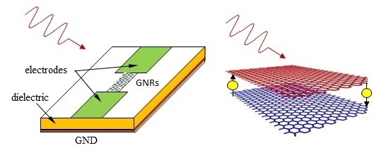
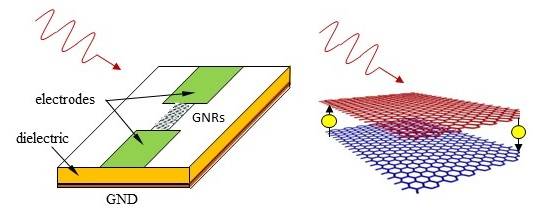
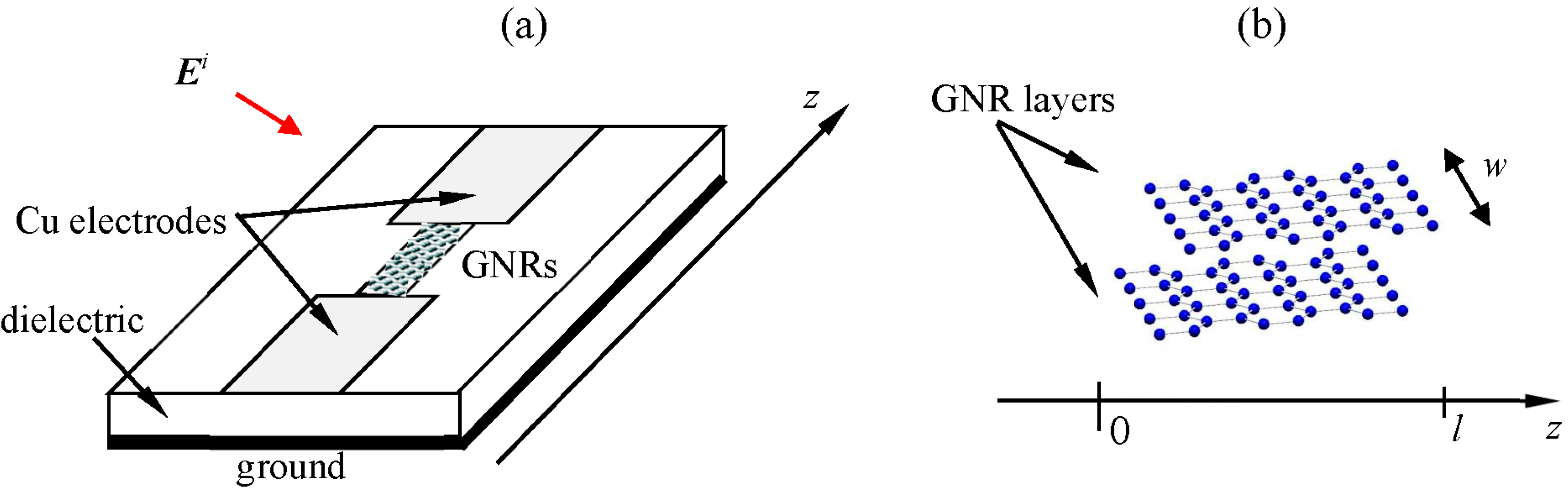
2. Electrical Response of a Bi-Layer Graphene Nanoribbon THz Detector

The THz detector proposed here is depicted in Figure 1, and is made as a microstrip-like circuit, where two copper electrodes are connected by bi-layer graphene nanoribbons. Figure 1a shows the entire device whereas, in Figure 1b, the bi-layer structure of the graphene nanoribbon contact is highlighted.
Figure 1. The proposed THz detector: (a) microstrip-like structure with a graphene contact; and (b) details of the few-layer graphene nanoribbons in the circuit gap.
Applsci 05 01102 g001
In view of studying the electrical properties of the GNR contact, we must include the effect of an external field in the electrodynamic model of the electrical transport along the z-axis of the multilayered structure in Figure 1b. This is will be done in this section by extending the model presented in [25,26,27,28]. To this end, we will start with a brief review of the transport model presented in the above references; then, we extend it to include the tunneling effect.

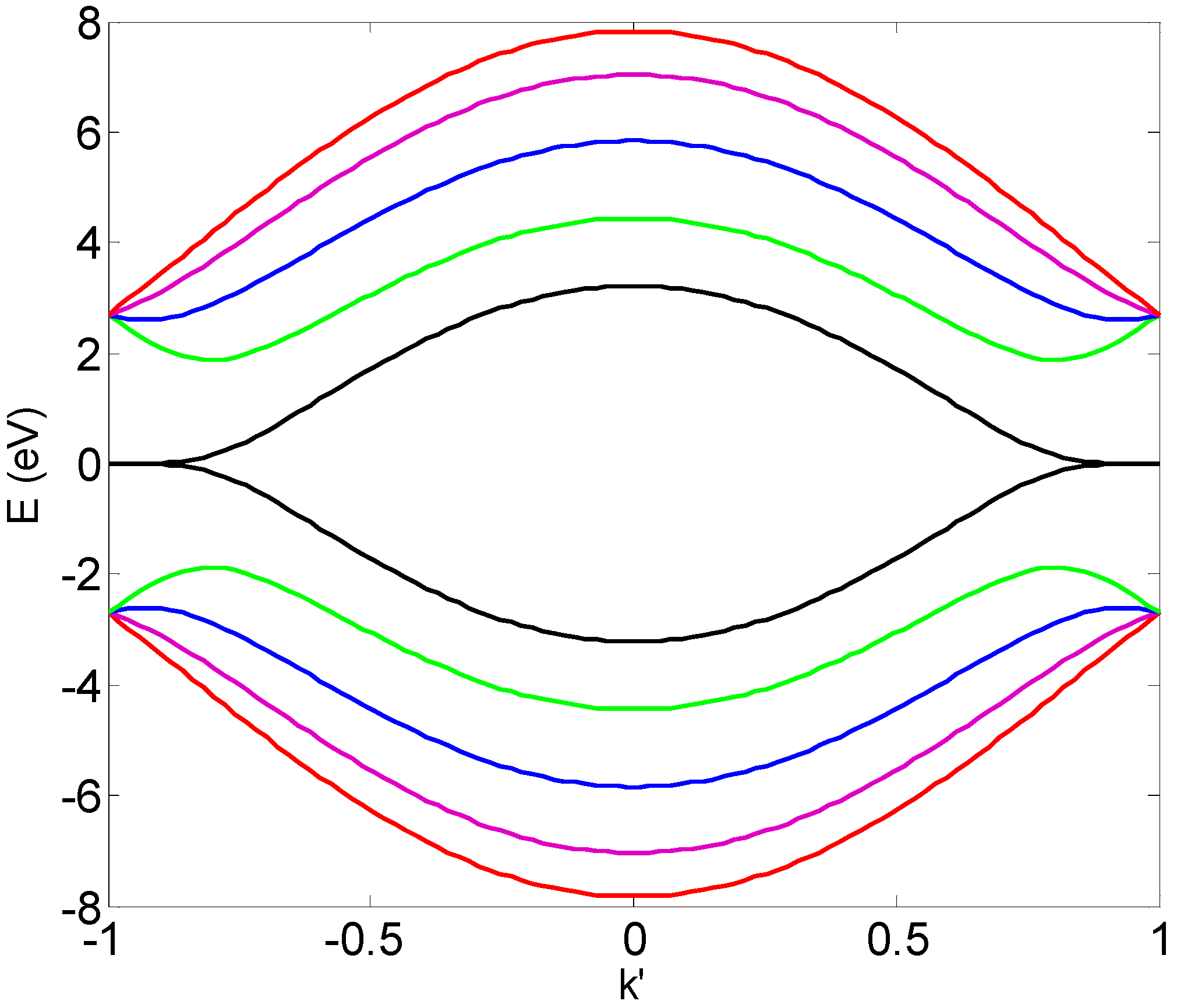
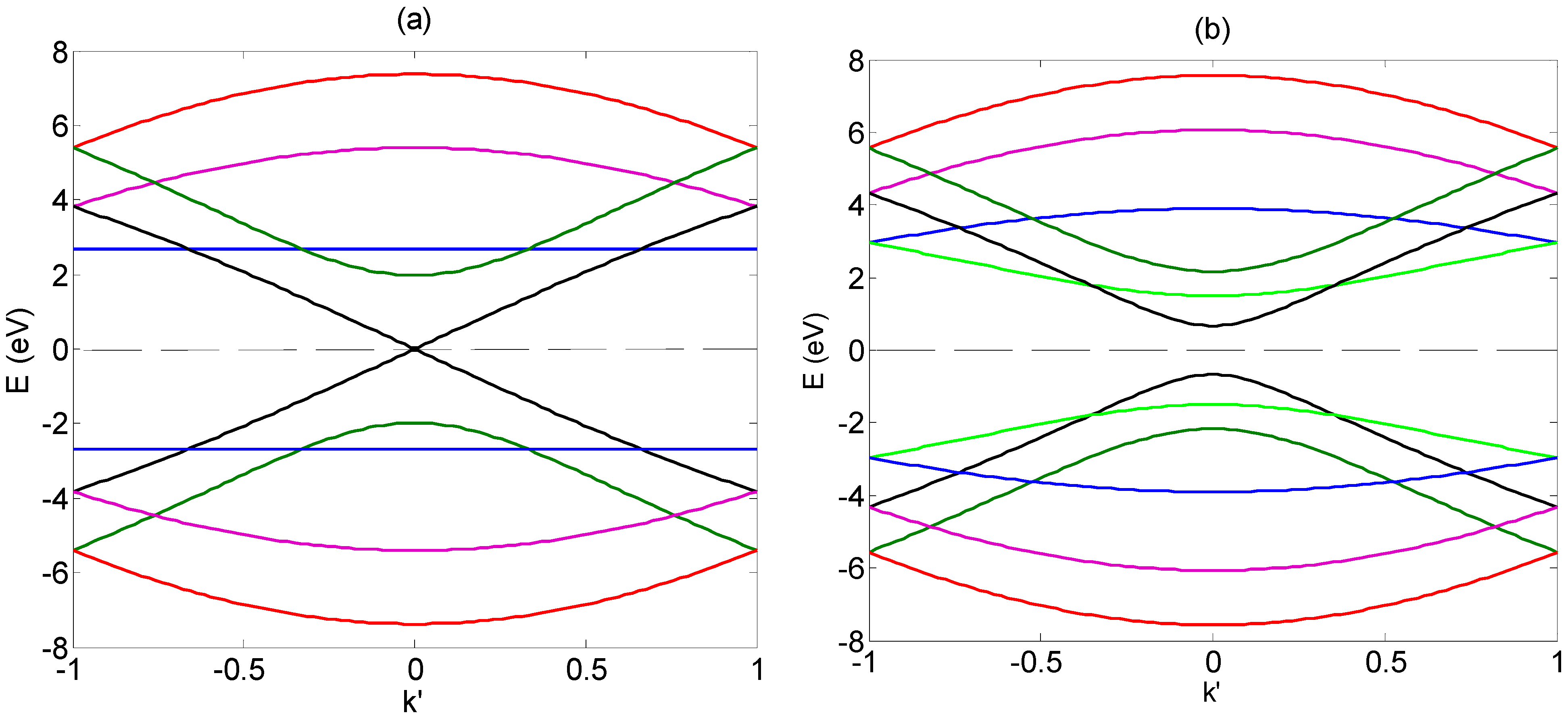
2.1. A Glimpse at the Graphene Nanoribbon Band Structure

The transport model presented in [25,26,27,28] is based on the knowledge of the band structure of the GNRs, which can be expressed in terms of the energy dispersion relation of the conduction electrons (the so-called π-electrons) in graphene [29]:
E ( ± ) ( k ) = ± γ [ 1 + 4 cos ( 3 k x a 0 2 ) cos ( k y a 0 2 ) + 4 cos 2 ( k y a 0 2 ) ] 1 / 2
where E ( ± ) is the energy (signs + and − denote the conduction and valence band, respectively), γ = 2.7 eV is the carbon-carbon interaction energy, and a 0 = 3 b is a lattice constant, being b = 1.42   Å the interatomic distance.
At equilibrium, the energy distribution function of π-electrons is given by the Dirac-Fermi function:
F [ E ( ± ) ] = 1 e E ( ± ) / k B T 0 + 1
where k B is the Boltzmann constant and T 0 is the absolute temperature.
Graphene nanoribbons are obtained by cutting a graphene layer in ribbons of a transverse width w much smaller than the longitudinal length (w << l, see Figure 1b). Two basic shapes may be obtained, “armchair” (A-GNR) or “zig-zag” (Z-GNR): they differ in the edges, which show a 30° difference in their orientation within the graphene sheet.
The width w of a graphene nanoribbon is directly related to the number of N dimers (two carbon sites) for the A-GNRs, and the number N of zig-zag lines for the Z-GNRs. The unit cell has translational length T = 3 a 0 ( T = a 0 ) and width w = N a 0 / 2 ( w = 3 N a 0 / 2 ) for A-GNRs (Z-GNRs).
In the nearest-neighbor tight-binding approximation, the dispersion relation of A-GNRs for the generic µ-th band is given by [30,31]:
E μ ( k ) = γ 1 + 2 ε μ cos ( k T / 2 ) + ε μ 2     for - π T k π T
where ε μ = 2 cos ( p μ ) , and the transverse wavenumber p μ is determined by the edge boundary condition:
p μ = μπ / ( N + 1 ) ,    μ = 1 , 2 , ... N .
For Z-GNRs the energy spectrum may not be given in closed form. However, in the nearest-neighbor tight-binding approximation, it can be derived by solving the eigenvalue problem [30,31]:
H ( k ) u = E ( k ) u
where H is a 2N × 2N symmetric sparse matrix that has nonzero elements only in the first diagonals below and above the main diagonal, defined as:
H j , j + 1 = γ { 2 cos ( a 0 k / 2 ) j   odd 1 j   even
Note that A-GNRs are metallic only for N = 3 q 1 , with q = 0,1,2,.., whereas for other values they are semiconducting. As for Z-GNRs, they have partially flat bands owing to the degeneration of edge states at k = ± π / T ; hence, their bandgap is always zero and their behavior is always metallic [31].
Figure 2 shows the typical band structures for A-GNRs, either in metallic and semiconducting cases. Figure 3, instead, reports the case of Z-GNRs.
Figure 2. Typical band structure for A-GNRs vs. normalized wavenumber k = k T / π : (a) metallic; and (b) semi-conducting.
Applsci 05 01102 g002
Figure 3. Typical band structure for Z-GNRs vs. normalized wavenumber k = k T / π .
Applsci 05 01102 g003

2.2. Transport Model along Graphene Nanoribbons, without the Tunneling Effect

The cross-section sizes of GNRs are typically large enough (at least 1 nm in the quantum confined directions) to have local crystal structures and to allow using the semi-classical transport model. Thus, the electrons are regarded as classical particles, which move under the action of a longitudinal electric field according to Boltzmann transport equation.
In the THz range we can assume that the following conditions hold:
(i)
the GNR width w is electrically small;
(ii)
the transverse currents may be neglected; and
(iii)
only intraband transitions are considered, whereas interband ones are not allowed.
Conditions (i) and (iii) are fully satisfied in the THz range, since the GNR width w is far below the minimum wavelength (0.03 mm at 10 THz), and the interband transitions occur at optical frequencies. Condition (ii) is fulfilled for large aspect-ratio GNRs.
Let us consider time-harmonic variation for the fields, expressed as X ( z , t ) = Re { X ^ z exp [ i ( ω t β z ) } , where β is the wavenumber, and let us indicate with J z ( z , t ) and E z ( z , t ) the longitudinal component of the current density and the electric field, respectively. The latter is written as:
E z ( z , t ) = E z i ( z , t ) + E z s ( z , t )
If the tunneling effect is neglected, the current density along the n-th signal line (n = 1,2) only depends on the electric field on the same line, and the following generalized Ohm’s law may be written in the wavenumber domain [32,33]:
J ^ z , n ( β , ω ) = σ ^ n ( β , ω ) E ^ z , n ( β , ω )     n = 1 , 2
where σ ^ n ( β , ω ) is the generalized longitudinal conductivity, which may be expressed as:
σ ^ n ( β , ω ) i 2 e 2 π 2 w v F 1 ω i ν n M n [ 1 + α n ( v F β ω i ν ) 2 ]
where e is the electron charge, is the Planck constant, v F the Fermi velocity, usually of the order of 10 6  m/s, and ν n is the collision frequency. The functions M n and α n appearing in Equation (9) are expressed in terms of the energy bands Equation (1), E μ , n ( ± ) and by their associated velocities v μ , n ( ± ) = d E μ , n ( ± ) / d ( k ) , according to:
M n = v F μ = 1 N 0 π / l [ v μ , n ( + ) 2 ( d F d E μ , n ( + ) ) + v μ , n ( ) 2 ( d F d E μ , n ( ) ) ] d k
α n = M n v F 3 μ = 0 N 1 0 π / l [ v μ , n ( + ) 4 ( d F d E μ , n ( + ) ) + v μ , n ( ) 4 ( d F d E μ , n ( ) ) ] d k
where F s the Dirac-Fermi distribution defined by Equation (2), M n represents the equivalent number of conducting channels, which depends on GNR chirality, width, and temperature, too, as shown in [27]. In the following, we assume that the two GNRs have the same chirality and width; therefore, all the parameters in Equations (8)–(11) are the same, in particular: M 1 = M 2 , α 1 = α 2 , and ν 1 = ν 2 .
Following the stream of [32,33], by coupling generalized Ohm’s law (8) to Maxwell’s equations it is possible to model the interconnects in Figure 2 as a lossy multiconductor transmission line (MTL), and, thus, the vectors of the spatial distributions of voltages, V ( z ) , and currents, I(z), are solutions of the telegraphers’ equations, which read in the frequency domain:
d V d z = ( R + i ω L ) I + V e q ,         d I d z = i ω C V + I e q
where V e q I e q represent two equivalent forcing terms related to the external impinging field:
V e q = i ωμ o l E z i ( z ) d z ,         I e q = i ω C o l H i ( z ) d z
The per-unit-length (p.u.l.) matrix parameters are given by [32,33,34]:
R = ν L k ( U + K ) 1 ,     L = ( L k U + L M ) ( U + K ) 1 ,    C = C E
where U is the unitary matrix, R, LM, and CE are the electrical resistance, magnetic inductance, and electrostatic capacitance matrices, respectively, whereas matrix K is given by:
K = C E 1 C q 1 1 i ν / ω
Here, the quantum nature of the electrodynamics is taken into account by the p.u.l. kinetic inductance, L k , and quantum capacitance, C q , given by:
L k = R 0 2 v M F ,       C q = v F 2 L k
being R 0 = 12.9  k Ω , the quantum resistance.
The properties of such a model are discussed in Section 3. Note that, in view of using the GNR pair as a single line (i.e., feeding them in parallel), it is possible to derive an equivalent single line model, for instance by following the approach in [35].

2.3. Transport Model along Graphene Nanoribbons, with the Tunneling Effect

In this paragraph, we extend the above model to include the possibility that the two GNRs may interact among them via the tunneling effect. In this case, we modify the generalized Ohm’s law (Equation (2)) taking into account the possible mutual interaction between the two GNRs:
{ J ^ z 1 = σ ^ 11 ( β , ω ) E ^ z 1 + σ ^ 12 ( β , ω ) E ^ z 2 , J ^ z 2 = σ ^ 21 ( β , ω ) E ^ z 1 + σ ^ 22 ( β , ω ) E ^ z 2 ,
where σ ^ 11 = σ ^ 22 = σ ^ s are the self-conductivities given as in Equation (2), whereas the mutual conductivities σ ^ 12 = σ ^ 21 = σ ^ m may be expressed as follows:
σ ^ m ( β , ω ) i 2 e 2 π v F X ω t ω β 2 1 1 ( β v F / ω ) 2 γ ^ ( β , ω )
where the complex frequency is defined as ω = ω + i ν , and
γ ^ ( β , ω ) = k = 1 , 2 ω β 2 2 ω t + ( 1 ) k [ 1 + ( β v F / ω ) 2 ] ( 2 ω t + ( 1 ) k ω ) β 2 v F 2
In the above relations, a fundamental role is played by the tunneling frequency ω t , related to the binding energy ω t due to delocalization of the π-electrons for the tunnel effect.
As a consequence of new constitutive relation Equation (17), the MTL model derived by coupling Equation (17) with Maxwell’s equation would be expressed through the p.u.l. matrix parameters obtained by adding to the inductance and capacitance matrices the operators L t u n ( I )   and C t u n ( V ) , acting as follows:
L t u n { I ( z , ω ) } = 1 4 π ω t ω ω v F ( c v F ) 2 Θ L M + K I ( z z ) I ( z , ω ) d z
C t u n 1 { V ( z , ω ) } = ω t ω 2 v F Θ C E 1 + K 2 ( z z ) V ( z , ω ) d z
where Θ is the matrix:
Θ = [ 1 1 1 1 ]
The kernels in Equation (20) are defined as
K 1 ( z ; ω ) = sin ( 2 ω t v F | z | ) exp ( i ω v F | z | )
K 2 ( z ; ω ) = 1 2 i exp ( i ω v F | z | ) [ 1 2 ω t ω exp ( i 2 ω t v F | z | ) + 1 2 ω t + ω exp ( i 2 ω t v F | z | ) ]
Note that the operator L t u n also adds to the kinetic inductance L k U in the modified expression of the resistance matrix R. Operator’s Equations (20) and (21) introduce a spatial and frequency dispersion, which affects the relations between the voltages and the p.u.l. charge and the currents, and the p.u.l. magnetic flux.

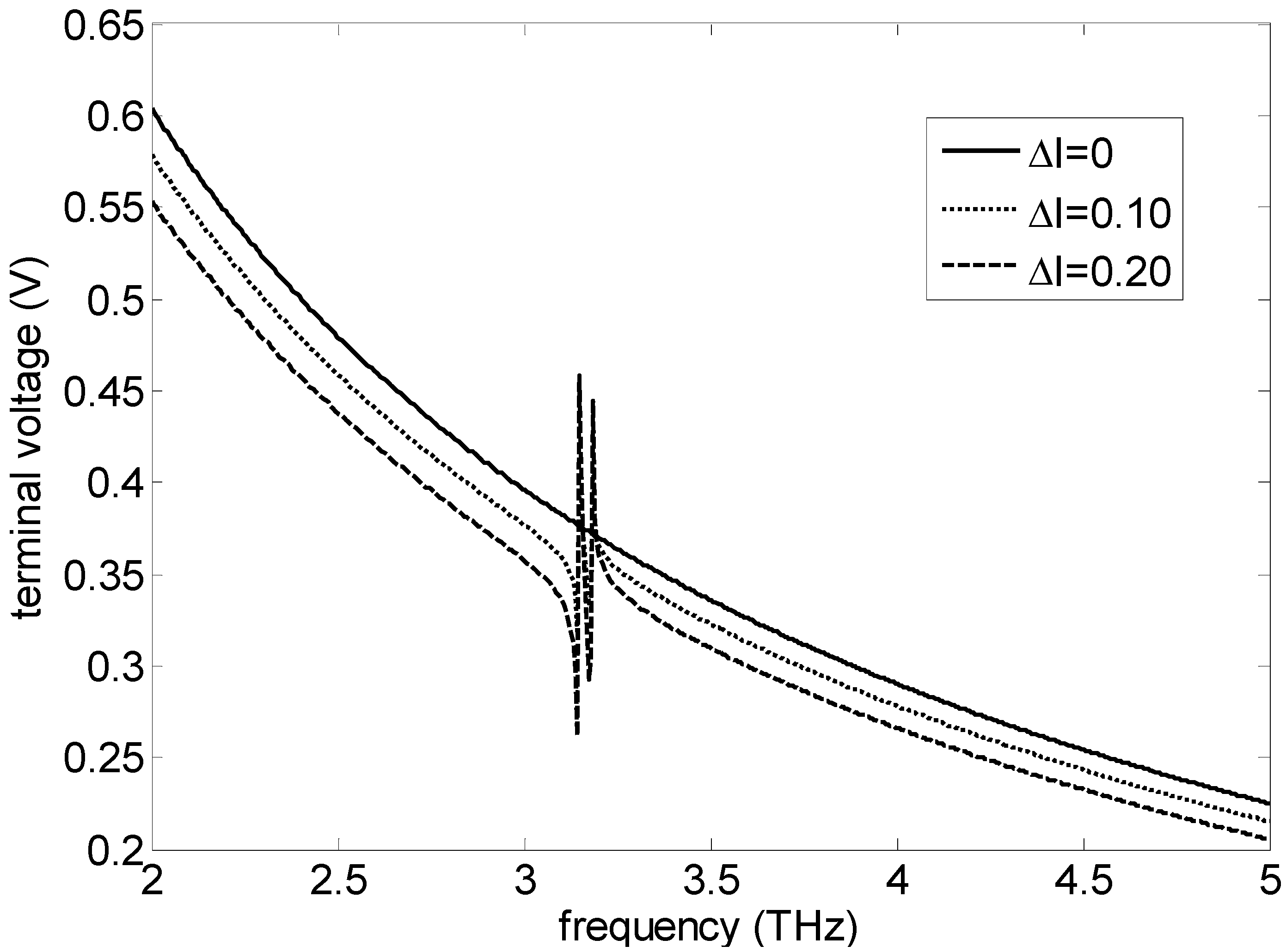
3. Discussion: Two Mechanisms of THz Resonance Excitation for the Proposed Detector

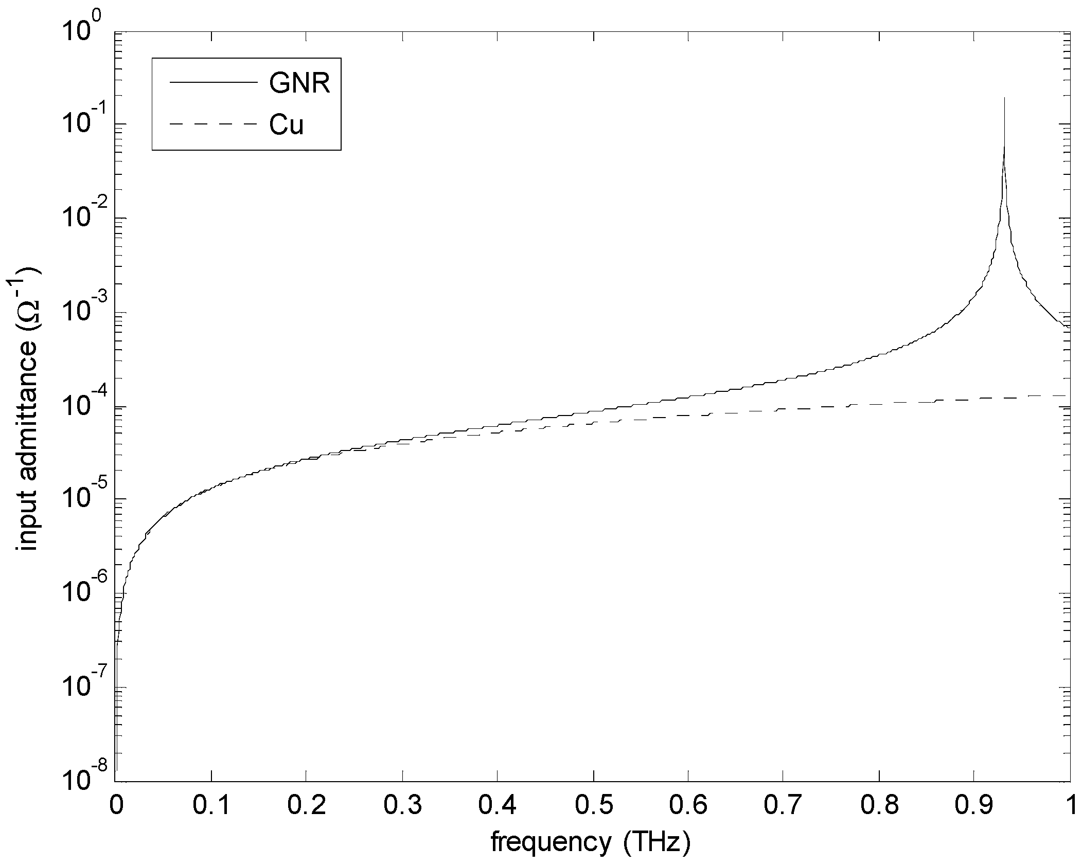
3.1. Interpretation of the THz Plasmon Resonances

The model presented here includes the possibility to excite plasmon resonances in the detector of Figure 1. This phenomenon can be also observed in the simpler case where only one GNR is used to contact the two electrodes; therefore, in the following we will assume a single GNR. In the absence of tunneling, the circuit model in Section 2.2 reduces to that of single lossy TL, with p.u.l. parameters given by:
R ν L k ,     L L k + L M ,    C = C E
These results hold because it is usually L k > > L M , C q < < C E , and the collision frequency is usually of the order of ν 10 12  Hz . A consequence of the huge value of the kinetic inductance is a low propagation velocity, c G N R , and a high characteristic impedance, Z C , G N R : typical values of these two parameters normalized to an ideally-scaled copper interconnect of the same dimensions would be:
c G N R c L m L k 10 2 ,   Z C N T Z C L k L m = 10 2
The plasmon resonances are then obtained by imposing the classical resonance condition along a transmission line, that is:
β l = n π / 2 ,   with n = 1 , 2 , 3
Let us refer to the detector in Figure 1a, assuming a metallic A-GNR, of width w = 2  nm and length l = 1 μm. The GNR lies on a dielectric layer of permittivity ε r = 2.2 and thickness 0.1 μm.
In the absence of external field, the TL model with p.u.l. parameters (Equation (25)) provides the input admittance reported in Figure 4, which clearly shows the existence of a plasmon resonance in the THz range. If the contact would be realized by copper instead of graphene, the higher propagation velocity would shift such a resonance to a frequency about two orders of magnitude higher, hence outside the THz range. This confirms a well-known result in the literature: in carbon-based nanostructures, by exciting the propagation of plasmons, i.e., such slowed down surface waves, it is possible to obtain resonances in the THz range, with reasonable lengths of the detector device [36,37,38]. Note that the high length/width ratio used in this example makes this configuration hard to be realized. According to Equation (27), reducing the length by a factor X means increasing the plasmon resonance frequency by the same factor. Therefore, to have plasmon resonance in the THz range we should fabricate a GNR with a minimum length of the order of about 100 nm.
Figure 4. Plasmon resonance in the input admittance of the detector in Figure 1, with a GNR of length 1 μm, compared to the case of Cu electrodes short-circuited.
Applsci 05 01102 g004

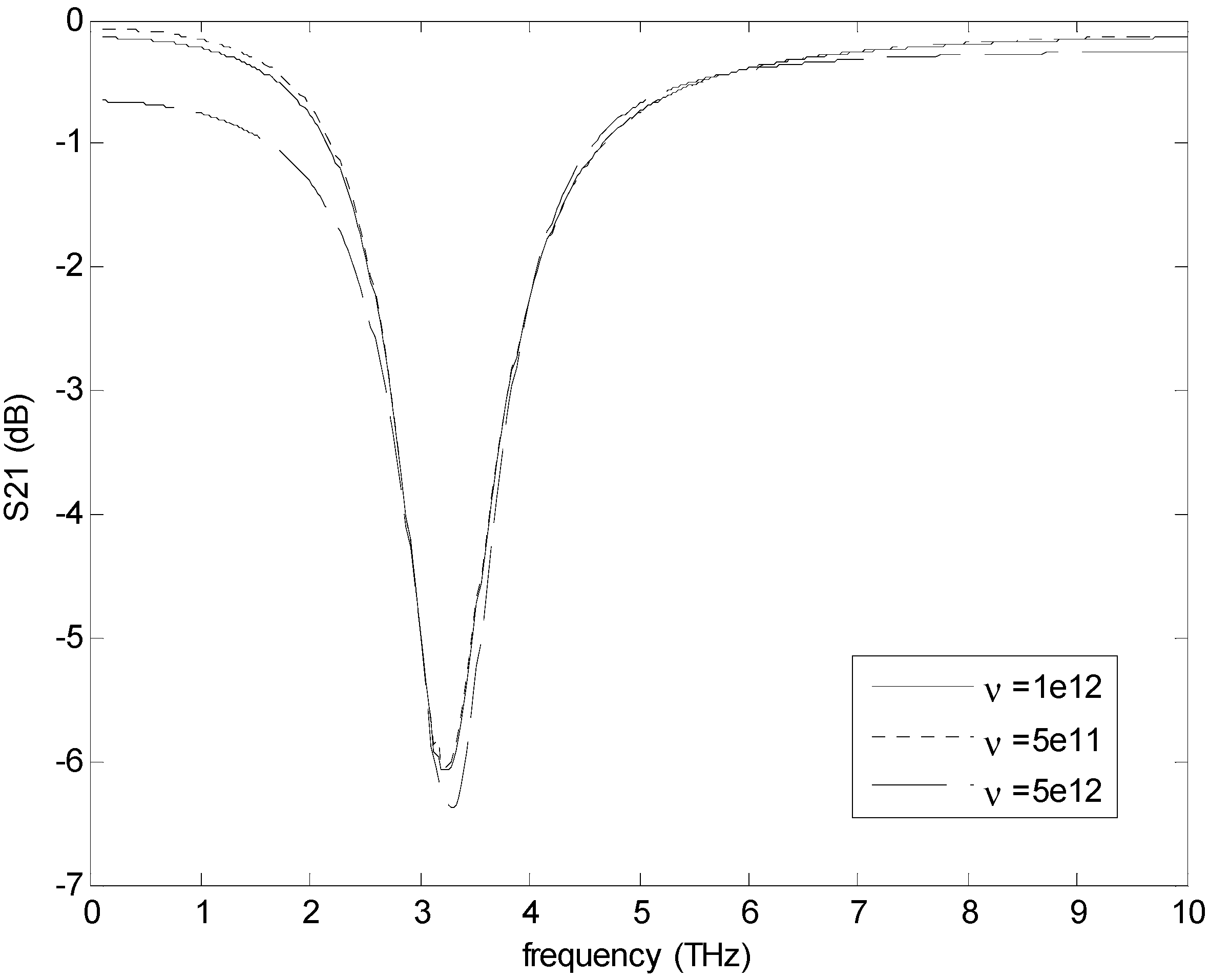
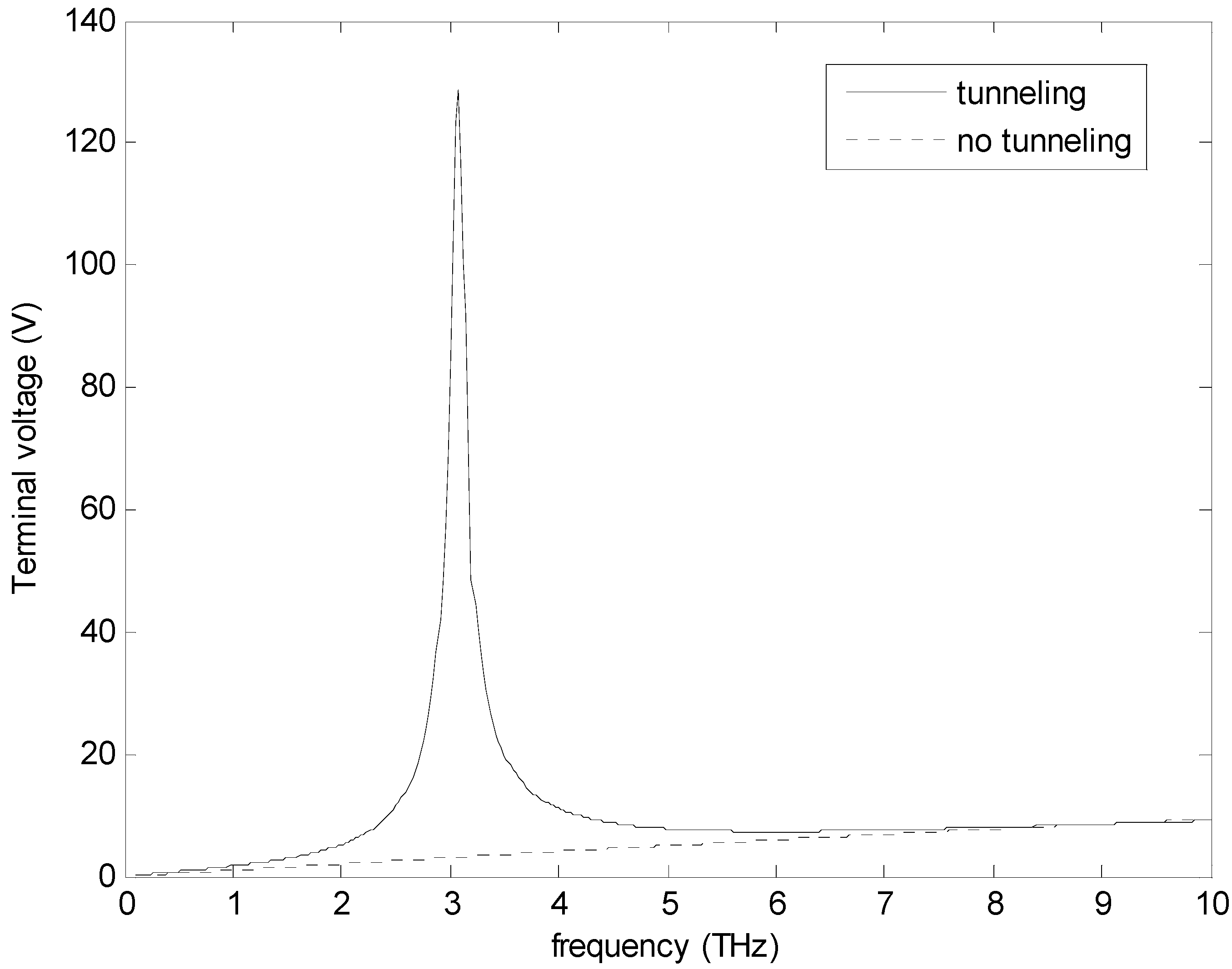
3.2. New THz Resonances for the Tunneling Effect

Let us now investigate a new mechanism of resonance excitation in the THz range, associated to the tunneling effect. To this end, we will refer to the detector in Figure 1a, assuming the contacts to be made by two metallic A-GNRs, of width w = 2  nm and length l = 50 nm. In addition, a dielectric layer of permittivity ε r = 2.2 and thickness 0.1 μm is considered. According to criterion Equation (27), for such a GNR length no plasmon resonances fall in the THz range.
To maximize the tunneling effect, we assume that the two GNR layers are separated by a minimum distance, namely the Van der Waals distance δ = 0.34  nm: for such a case, a measured value of binding energy of ω t 35  meV was reported, which corresponds to a tunneling frequency of ω t 10 13  rad/s [34]. The binding energy and, thus, the tunneling frequency, may be varied by changing the interlayer distance [39] or intercalating the layers with dopants, or even rotating the GNRs to form an angle, in order to excite the so-called chiral or Klein tunneling effect [40]. All these mechanism could be investigated in view of realizing multi-frequency detectors.
For the sake of simplicity, we consider the impinging external field, E i , to be a time-harmonic plane-wave with a wave-vector orthogonal to the z-axis. The general case of a field hitting the detector with any other angle may be handled by projecting the field in the plane of the detector.
To solve MTL equations, let us focus on the effect of the additional term L t u n Equation (20), assuming that the quantum capacitance is such that in Equation (14) it is U + K U . Having assumed a length below 100 nm, in the THz range the line is electrically short and it is possible to disregard the spatial variation of the distribution of the currents along it. In other words, we can neglect the spatial dispersion introduced by Equation (20) and focus on the frequency dispersion. In addition, since ν 10 12  Hz, in the THz range it is also ω ω . As a consequence, the tunneling operator Equation (20) may be approximated as:
L t u n ( I ( ω ) ) 1 π ( c v F ) 2 ω t 2 4 ω t 2 ω 2 [ 1 1 1 1 ] L M I ( ω )
Therefore, the tunneling effect introduces a singularity in operator (Equation (28), for a frequency ω = 2 ω t . This singularity is responsible for a resonance peak in the response of the device.
For instance, Figure 5 shows the absolute value of the line transmission coefficient (i.e., the scattering parameter | S 21 ( ω ) | ), assuming a matched load condition, in the absence of an external field. Without the tunneling effect, this coefficient exhibits the expected behavior for a matched load, but in the presence of tunneling there is a pronounced absorption peak corresponding to the abovementioned frequency f r = 2 ω t / 2 π 3.2  THz . The peak width can be modulated by the collision frequency, as shown in Figure 6.
Figure 5. Transmission coefficient | S 21 ( ω ) | for GNR lines with matched loads, in the absence of external fields, with or without the tunneling effect.
Applsci 05 01102 g005
Figure 6. Modulation of the width of absorption peak in the transmission coefficient | S 21 ( ω ) | , due to the collision frequency.
Applsci 05 01102 g006
Such a behavior may be exploited for using the circuit in Figure 1a as a detector. To this end, let us assume that the external field E i induces currents only on the outermost GNR layer, being the inner one shielded by it. This is reasonable, if we take into account the extremely short distance between the two GNR layers. In this case, we can solve the MTL Equation (12) in Section 2, assuming that the source terms V e q ,   I e q are only active on the outer line (say, Line 1), whereas they are put to zero on the other line (say, Line 2):
V e q = [ V 1 , e q   0] T ,      I e q = = [ I 1 , e q   0] T
Let us assume that the circuit is illuminated by the external field and the line is left open-circuit at both ends. The external field is chosen such to induce a current of 0.2 mA along the outer line (Line 1). In Figure 7 we plot the voltages obtained at the two ends of the GNR contacts for varying values of the frequency of impinging field, with or without the tunneling effect. The result suggests the possibility of detecting an incoming field in the THz range, thanks to the resonance effect due to tunneling.
The possibility of exciting these resonances is strictly related to the unbalanced currents flowing in the two lines, as in the proposed case. The opposite case would be that of assuming that the external field induces exactly the same current on the two lines, i.e., a pure common mode current is excited. In this case, the self and mutual terms related to tunneling cancel themselves. This result is shown in Figure 8, where the terminal voltages are calculated in presence of a common current of 0.01 mA excited by the external field. The resonance peak appears again only if the currents are misbalanced, as shown by the results in Figure 8, referring to different values of the relative difference Δ I = | ( I 1 I 2 ) | / | I 2 | .
Figure 7. Terminal voltages at the ends of GNR contacts (see Figure 1a) illuminated by an external field, as a function of its frequency.
Applsci 05 01102 g007
Figure 8. Resonance peaks for balanced and misbalanced currents.
Applsci 05 01102 g008

4. Conclusions

In this paper we have investigated a new possible mechanism to detect signals in the THz range, based on the tunneling effect between two adjacent graphene nanoribbons. The electrodynamic transport model along a line made by a GNR pair above a ground plane is obtained by generalizing an existing model based on the semi-classical solution of the Boltzmann equation. The generalization proposed here allows including the transverse coupling between two adjacent GNRs, imposed by tunneling effect.
The final circuit model is written in the frame of the multiconductor transmission lines, where the tunneling effect introduces new operators which must be taken into account in the general expressions of the model parameters: resistance, inductance, and capacitance. These operators introduce in the model a spatial and frequency dispersion, and in particular, a singularity corresponding to a frequency value related to the tunneling frequency. For typical GNR dimensions, this phenomenon leads to a resonance peak in the response of the line in the THz range.
The model is also able to predict the existence of the well-known plasmon resonance in the THz range: it is shown that the new resonances associated with the tunneling may be observed for line lengths such that no plasmon resonance may occur in the THz range. Finally, it is shown that the GNR pair may be used to detect a THz wave provided that the system must be designed in such a way that the current excited in one GNR layer by the external field is not exactly the same as that excited in the other layer. This can be obtained by the shielding effect of the outermost layer with respect to the innermost one. The best condition for detector sensitivity will be having one layer completely shielded by the other one. To this end, future work will be devoted to designing a new configuration of electrodes to contact the two layers separately.

Acknowledgments

The work was partially supported by GRAPHENE-Graphene-Based Revolutions in ICT and Beyond, project n.604391 FP7-ICT-2013-FET-F.

Conflicts of Interest

The author declares no conflict of interest.

References

  1. Siegel, P.H. Terahertz technology. IEEE Trans. Microw. Theory Technol. 2002, 50, 910–928. [Google Scholar] [CrossRef]
  2. Ferguson, B.; Zhang, X.C. Materials for terahertz science and technology. Nat. Mater. 2002, 1, 26–33. [Google Scholar] [CrossRef] [PubMed]
  3. Kiyomi, S. Terahertz Optoelectronics; Springer: Berlin, Germany, 2005. [Google Scholar]
  4. Lee, G.M.; Wanke, M.C. Searching for a solid-state terahertz technology. Science 2007, 316, 64–65. [Google Scholar] [CrossRef] [PubMed]
  5. Hartmann, R.R.; Kono, J.; Portnoi, M.E. Terahertz science and technology of carbon nanomaterials. Nanotechnology 2014. [Google Scholar] [CrossRef]
  6. Li, H.; Xu, C.; Srivastava, N.; Banerjee, K. Carbon Nanomaterials for Next-Generation Interconnects and Passives: Physics, Status, and Prospects. IEEE Trans. Electron. Devices 2009, 56, 1799–1821. [Google Scholar] [CrossRef]
  7. Chen, X.; Akinwande, D.; Lee, K.-J.; Close, G.F.; Yasuda, S.; Paul, B.C.; Fujita, S.; Kong, J.; Wong, H.-S.P. Fully Integrated Graphene and Carbon Nanotube Interconnects for Gigahertz High-Speed CMOS Electronics. IEEE Trans. Electron. Devices 2010, 57, 3137–3143. [Google Scholar] [CrossRef]
  8. Van Noorden, R. Moving towards a graphene world. Nature 2006, 442, 228–229. [Google Scholar] [CrossRef] [PubMed]
  9. Avouris, P.; Chen, Z.; Perebeinos, V. Carbon-based electronics. Nat. Nanotechnol. 2007, 2, 605–615. [Google Scholar] [CrossRef] [PubMed]
  10. Renteria, J.D.; Nika, D.L.; Balandin, A.A. Graphene Thermal Properties: Applications in Thermal Management and Energy Storage. Appl. Sci. 2014, 4, 525–547. [Google Scholar] [CrossRef]
  11. Berres, J.A.; Hanson, G.W. Multiwall carbon nanotubes at RF-THz frequencies: Scattering, shielding, effective conductivity, and power dissipation. IEEE Trans. Antennas Propag. 2011, 59, 3098–3103. [Google Scholar] [CrossRef]
  12. Batrakov, K.; Kibis, O.V.; Kuzhir, P.; da Costa, M.R.; Portnoi, M.E. Terahertz processes in carbon nanotubes. J. Nanophotonics 2010. [Google Scholar] [CrossRef]
  13. Lin, I.-T.; Lai, Y.P.; Wu, K.-H.; Liu, J.M. Terahertz Optoelectronic Property of Graphene: Substrate-Induced Effects on Plasmonic Characteristics. Appl. Sci. 2014, 4, 28–41. [Google Scholar] [CrossRef]
  14. Brun, C.; Wei, T.C.; Franck, P.; Chong, Y.C.; Lu, C.; Leong, C.W.; Tan, D.; Kang, T.B.; Coquet, P.; Baillargeat, D. Carbon nanostructures dedicated to millimeter-wave to THz interconnects. IEEE Trans. Terahertz Sci. Technol. 2015, 5, 383–390. [Google Scholar] [CrossRef]
  15. Burke, P.J. AC performance of nanoelectronics: Towards a ballistic THz nanotube transistor. Solid-State Electron. 2004, 48, 1981–1986. [Google Scholar] [CrossRef]
  16. Shuba, M.V.; Slepyan, G.Y.; Maksimenko, S.A.; Thomsen, C.; Lakhtakia, A. Theory of multiwall carbon nanotubes as waveguides and antennas in the infrared and the visible regimes. Phys. Rev. B 2009. [Google Scholar] [CrossRef]
  17. Hanson, G.W. Fundamental transmitting properties of carbon nanotube antennas. IEEE Trans. Antennas Propag. 2005, 53, 3426–3435. [Google Scholar] [CrossRef]
  18. Rana, F. Graphene terahertz plasmon oscillators. IEEE Trans. Nanotechnol. 2008, 7, 91–99. [Google Scholar] [CrossRef]
  19. Kibis, O.V.; da Costa, M.R.; Portnoi, M.E. Generation of terahertz radiation by hot electrons in carbon nanotubes. Nano Lett. 2007, 7, 3414–3417. [Google Scholar] [CrossRef] [PubMed]
  20. Slepyan, G.Y.; Shuba, M.V.; Maksimenko, S.A.; Lakhtakia, A. Theory of optical scattering by achiral carbon nanotubes and their potential as optical nanoantennas. Phys. Rev. B 2006. [Google Scholar] [CrossRef]
  21. Burke, P.J.; Li, S.; Yu, Z. Quantitative theory of nanowire and nanotube antenna performance. IEEE Trans. Nanotechnol. 2006, 5, 314–334. [Google Scholar] [CrossRef]
  22. Llatser, I.; Kremers, C.; Chigrin, D.N.; Jornet, J.M.; Lemme, M.C.; Cabellos-Aparicio, A.; Alarcon, E. Radiation characteristics of tunable graphennas in the terahertz band. Radioengineering 2012, 21, 946–953. [Google Scholar]
  23. Zhang, Q.; Hároz, E.H.; Jin, Z.; Ren, L.; Wang, X.; Arvidson, R.S.; Lüttge, A.; Kono, J. Plasmonic nature of the terahertz conductivity peak in single-wall carbon nanotubes. Nano Lett. 2013, 13, 5991–5996. [Google Scholar] [CrossRef] [PubMed]
  24. Magda, G.Z.; Jin, X.; Hagymási, I.; Vancsó, P.; Osváth, Z.; Nemes-Incze, P.; Hwang, C.; Biró, L.P.; Tapasztó, L. Room-temperature magnetic order on zigzag edges of narrow graphene nanoribbons. Nature 2014, 514, 608–611. [Google Scholar] [CrossRef] [PubMed]
  25. Maffucci, A.; Miano, G. Transmission line model of graphene nanoribbon interconnects. Nanosci. Nanotechnol. Lett. 2013, 5, 1207–1216. [Google Scholar] [CrossRef]
  26. Maffucci, A.; Miano, G. Electrical Properties of Graphene for Interconnect Applications. Appl. Sci. 2014, 4, 305–317. [Google Scholar] [CrossRef]
  27. Maffucci, A.; Miano, G. Number of conducting channels for armchair and zig-zag graphene nanoribbon interconnects. IEEE Trans. Nanotechnol. 2013, 12, 817–823. [Google Scholar] [CrossRef]
  28. Chiariello, A.G.; Maffucci, A.; Miano, G.A. Circuit models of carbon-based interconnects for nanopackaging. IEEE Trans. Componen. Packag. Manufact. 2013, 3, 1926–1937. [Google Scholar] [CrossRef]
  29. Neto, A.H.C.; Guinea, F.; Peres, N.M.R.; Novoselov, K.S.; Geim, A.K. The electronic properties of grapheme. Rev. Modern Phys. 2009. [Google Scholar] [CrossRef]
  30. Wakabayashi, K.; Sasaki, K.; Nakanishi, T.; Enoki, T. Electronic states of graphene nanoribbons and analytical solutions. Sci. Technol. Adv. Mater. 2010. [Google Scholar] [CrossRef]
  31. Nakada, K.; Fujita, M.; Dresselhaus, G.; Dresselhaus, M.S. Edge state in graphene ribbons: Nanometer size effect and edge shape dependence. Phys. Rev. B 1996, 54, 17954–17961. [Google Scholar] [CrossRef]
  32. Miano, G.; Forestiere, C.; Maffucci, A.; Maksimenko, S.A.; Slepyan, G.Y. Signal propagation in single wall carbon nanotubes of arbitrary chirality. IEEE Trans. Nanotechnol. 2011, 10, 135–149. [Google Scholar] [CrossRef]
  33. Maffucci, A.; Miano, G. A general frame for modeling the electrical propagation along graphene nanoribbons, carbon nanotubes and metal nanowires. Comput. Modell. New Technol. 2015, 19, 8–14. [Google Scholar]
  34. Forestiere, C.; Maffucci, A.; Maksimenko, S.A.; Miano, G.; Slepyan, G.Y. Transmission line model for multiwall carbon nanotubes with intershell tunneling. IEEE Trans. Nanotechnol. 2012, 11, 554–564. [Google Scholar] [CrossRef]
  35. Cui, J.-P.; Zhao, W.-S.; Yin, W.-Y.; Hu, J. Signal Transmission Analysis of Multilayer Graphene Nano-Ribbon (MLGNR) Interconnects. IEEE Trans. Electromagn. Compat. 2012, 54, 126–132. [Google Scholar] [CrossRef]
  36. Slepyan, G.Y.; Shuba, M.V.; Maksimenko, S.A.; Thomsen, C.; Lakhtakia, A. Terahertz conductivity peak in composite materials containing carbon nanotubes: Theory and interpretation of experiment. Phys. Rev. B 2010. [Google Scholar] [CrossRef]
  37. Batrakov, K.G.; Saroka, V.A.; Maksimenko, S.A.; Thomsen, C. Plasmon polariton slowing down in graphene structures. J. Nanophotonics 2012. [Google Scholar] [CrossRef]
  38. Morimoto, T.; Joung, S.-K.; Saito, T.; Futaba, D.N.; Hata, K.; Okazaki, T. Length-dependent plasmon resonance in single-walled carbon nanotubes. ACS Nano 2014, 8, 9897–9904. [Google Scholar] [CrossRef] [PubMed]
  39. Ohta, T.; Bostwick, A.; Seyller, T.; Horn, K.; Rotenberg, E. Controlling the Electronic Structure of Bilayer Graphene. Science 2006, 313, 951–954. [Google Scholar] [CrossRef] [PubMed]
  40. Katsnelson, M.I.; Novoselov, K.S.; Geim, A.K. Chiral tunnelling and the Klein paradox in grapheme. Nat. Phys. 2006, 2, 620–625. [Google Scholar] [CrossRef] [Green Version]

