There are many types of electrically small planar resonators. In this paper, the main focus will be on those resonators of interest for the design of metamaterials or metamaterial-based or inspired microwave circuits and antennas. The list may be too long, hence, it will be limited to the more relevant and useful implementations, according to the authors own experience.
3.1. Topologies and Circuit Models of the Isolated Resonators
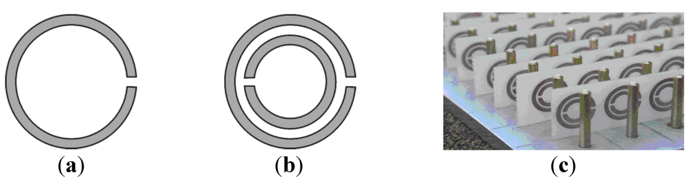
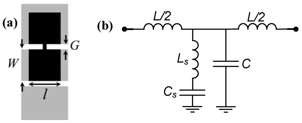
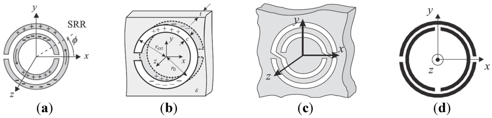
Let us begin with the SRR already considered in the previous section [
12]. As long as the distance between both rings is small (
i.e., there is significant coupling between them), the particle can be considered to be electrically small and a quasi-static analysis to infer the SRR inductance and capacitance can be applied. Such an analysis was carried out in [
7,
15]. When the SRR is excited by an external time-varying magnetic field directed along the SRR axis (
z-axis in
Figure 3), the cuts on each ring force the electric current to flow from one ring to another across the slot between them, taking the form of a strong displacement current. The slot between the rings therefore behaves as a distributed capacitance, and the whole SRR has the equivalent circuit shown in
Figure 3(b), where
Ls is the SRR self-inductance and
Co/2 is the capacitance associated with each SRR half. This capacitance is
Co = 2π
roCpul, where
ro is the mean radius of the SRR, and
Cpul is the per unit length capacitance along the slot between the rings. The total capacitance of this circuit is the series connection of the capacitance of both SRR halves, that is,
Co/4. Therefore, the resonance frequency
ωo is given by:
The inductance
Ls can be modeled as the inductance of an average ring of radius
ro,
i.e., the mean radius of the ring, and width
c. Approximate expressions for
Ls, based on a variational calculation, are provided in [
16]. Closed expressions for the per unit length capacitance are given in many microwave textbooks [
17], and explicit expressions for
Ls and
Cpul are provided in [
7].
The model of
Figure 3 is valid as long as the perimeter of the ring can be considered small with regard to half wavelength, and the capacitance associated with the cuts on each ring can be neglected. Under such assumptions, the currents on each ring must vanish at the cuts, and the angular dependence of the currents on each ring can be assumed to be linear (so that the total current on both rings is constant). Such assumptions also imply that the voltage across the slots is constant in both SRR halves. A more detailed circuit model, which takes into account the gap capacitance and includes a transmission line model for the slot between the rings has been reported in [
18], but such a model converges to the model of
Figure 3 when the capacitance of the cuts is neglected and the electrical length of the SRR is small [
18]. As both approximations are usually fulfilled for any practical SRR design, the more simple model reported above is assumed valid in this paper.
Figure 3.
SRR topology and its equivalent circuit model.
Figure 3.
SRR topology and its equivalent circuit model.
The closer the rings of the SRR of
Figure 3 are the lower the resonance frequency and the smaller the electrical size of the particle result. However, in practice, the separation between rings cannot be smaller than a certain value that depends on the fabrication technology (typically 100 µm for PCB technology). This means that the electrical size of edge coupled SRRs cannot be reduced below roughly
λ/10. To circumvent this limiting aspect, one possible solution is to print the rings face-to-face on opposite sides of a thin dielectric slab. Whilst this modification does not significantly affect the behavior of the resonator, the per unit length capacitance (
i.e., the capacitance of the broadside coupled strips) is markedly increased, and hence the particles can be made as small as
λ/30 [
15], or even smaller. Obviously, the penalty of these broadside coupled split ring resonators (BC-SRRs) is the need of two metallic levels for their implementation.
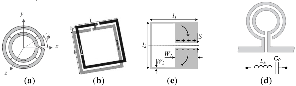
There is, however, another interesting aspect that differentiates the conventional SRR and the BC-SRR. The charge distribution in the SRR (depicted in
Figure 4(a)) indicates that there is an electric dipole at the first resonance frequency in the orthogonal direction to the symmetry plane of the particle (such a symmetry plane is an electric wall). This means that the SRR can also be excited by means of a time varying electric field applied in the plane of the particle co-directional to the direction of the electric dipole. Hence, the first SRR resonance can be driven electrically and/or magnetically,
i.e., the particle exhibits bianisotropy. For the BC-SRR, charges in the upper half are also images of charges in the lower half, but this charge distribution does not result in a net dielectric dipole (
Figure 4(b)). Thus, the BC-SRR is non-bianisotropic. Another possible way to avoid bianisotropy while keeping a uniplanar design is by means of the topology depicted in
Figure 4(c) [
19]. Essentially, the circuit model of this particle, called non-bianisotropic split ring resonator (NB-SRR), is that of the conventional SRR. However, the NB-SRR, like the BC-SRR, has an inversion symmetry with regard to its center, which means that cross polarization effects are not present,
i.e., the first resonance frequency cannot be excited through an electric field.
An alternative way to obtain inversion symmetry, thus overcoming bianisotropy is by introducing additional cuts in the edge coupled SRR, as
Figure 4(d) illustrates [
19]. This particle, called double slit split ring resonator DS-SRR, exhibits the same inductance as the SRR, but its capacitance is four times smaller since it is the result of the series connected edge capacitances of each SRR quarter. This means that the resonance frequency is twice the resonance frequency of the SRR, and hence the electrical size of the particle cannot be made very small.
Figure 4.
Topology and charge distribution of (a) conventional SRR, (b) broadside coupled split ring resonators (BC-SRR), (c) non-bianisotropic split ring resonator (NB-SRR), and (d) double slit split ring resonator (DS-SRR).
Figure 4.
Topology and charge distribution of (a) conventional SRR, (b) broadside coupled split ring resonators (BC-SRR), (c) non-bianisotropic split ring resonator (NB-SRR), and (d) double slit split ring resonator (DS-SRR).
Another interesting particle that combines the advantages of small electrical size and uniplanar configuration is the spiral. The two-turn spiral 2-SR can be considered to be constituted of two rings with cuts in the same position and with an electric short between both rings through cross terminals, as shown in
Figure 5(a). A quasistatic analysis of this particle [
20,
21] reveals that the inductance is that of the SRR with identical dimensions. However, the capacitance is the edge capacitance of the whole circumference. Therefore, the resonance frequency is half the resonance frequency of the SRR. Spirals are therefore very useful in applications where small electrical size combined with a monolayer design is required. Obviously, it is possible to etch the two spiral loops at different levels, one on top of the other, connected through a metallic via [
22]. Although the price to pay in this case is the use of two metal levels, this broad side coupled spiral resonator (BC-SR, see
Figure 5(b)) exhibits a very small electrical size if the metal levels are separated by a very thin dielectric layer (with this design, particle diameters as small as
λ/100 can be achieved).
Figure 5.
Topology of the (a) two-turn spiral resonator (2-SR), (b) BC-SR, (c) folded stepped impedance resonator (SIR) and (d) open split ring resonator (OSRR) (including the circuit model).
Figure 5.
Topology of the (a) two-turn spiral resonator (2-SR), (b) BC-SR, (c) folded stepped impedance resonator (SIR) and (d) open split ring resonator (OSRR) (including the circuit model).
Another interesting electrically small planar particle is the stepped impedance resonator (SIR). It is well known that the length of a
λ/2 resonator can be reduced by narrowing and widening the central and outer sections, respectively, of the particle [
23]. If, additionally, we fold it, as depicted in
Figure 5(c), the edge capacitance between the patches enhances the capacitance of the particle and hence the electrical length is made smaller. The folded SIR exhibits bianisotropy and combined with transmission lines is very interesting in order to achieve extremely small devices, as will be shown later.
The previous particles are closed particles that can be magnetically and, in some cases, electrically driven. Open particles can also be of interest in applications where the resonator must be excited by means of a voltage or current source. Inspired by the topology of the SRR of
Figure 3, the open split ring resonator (OSRR) was presented in 2004 [
24]. This particle can be constructed by means of two concentric rings with cuts in the same position. By elongating the rings, shaping them as a hook (
Figure 5(d)), we create the two required terminals for particle excitation. The incident current is transferred from one ring to the other through the distributed edge capacitance between the two rings. According to that, it is clear that the resonance frequency of this series resonator is identical to the resonance frequency of the two-turn spiral resonator, 2-SR. Therefore OSRRs are very interesting for applications where small series (open) resonators implemented in one metal layer are required. Indeed, the OSRR, rather than an open SRR, is an open 2-SR. However, we will preserve the original term assigned to this particle in [
24].
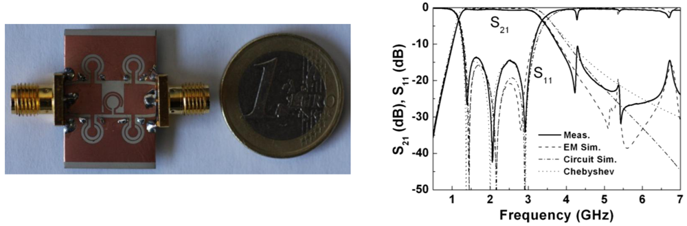
Concerning open SIRs, the SISS reported in
Section 2 is indeed an open version of the SIR. It is an open series resonator shunt connected to the host microstrip line. Open SIRs can also be implemented in CPW structures by etching this particle in the back substrate side, with the wide strip sections below the central strip and ground planes. This enhances the electric coupling between the line and the SIR and hence very small resonance frequencies can be achieved with small particles. Therefore, electrically driven open SIRs can be made electrically very small.
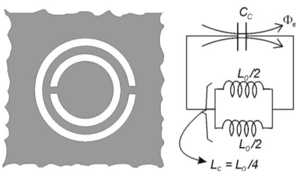
Let us now consider the application of duality to some of the previous particles. If the topology of the SRR is removed from a metallic film, the resulting particle (
Figure 6) can be considered the negative image, or the complementary counterpart, of the SRR. For this reason, this particle has been called complementary split ring resonator (CSRR) [
25]. It can be easily demonstrated by applying the Babinet principle, that the CSRR can be excited by means of an axial time varying electric field or by means of a magnetic field applied to the plane of the particle [
26]. Under ideal conditions,
i.e., a perfectly conducting and zero-thickness metallic screen, it can be demonstrated that the resonance frequency of the CSRR is identical to the resonance frequency of the SRR (provided identical dimensions and substrate are considered). Indeed, the capacitance of the CSRR,
Cc, is the capacitance of a disk of radius
ro−
c/2 surrounded by a ground plane at a distance
c of its edge. The inductance is given by the parallel connection of the two inductances of the metallic strips connecting the inner and outer metallic regions of the CSRR. These inductive values are given by
Lo/2, where
Lo = 2π
rLpul, with
Lpul being the per unit length inductance of the CPWs connecting the inner disk to ground.
Figure 6.
Complementary split ring resonator (CSRR) topology and its equivalent circuit model. Geometrical parameters of the CSRR are identical to those of
Figure 3 referred to the SRR.
Figure 6.
Complementary split ring resonator (CSRR) topology and its equivalent circuit model. Geometrical parameters of the CSRR are identical to those of
Figure 3 referred to the SRR.
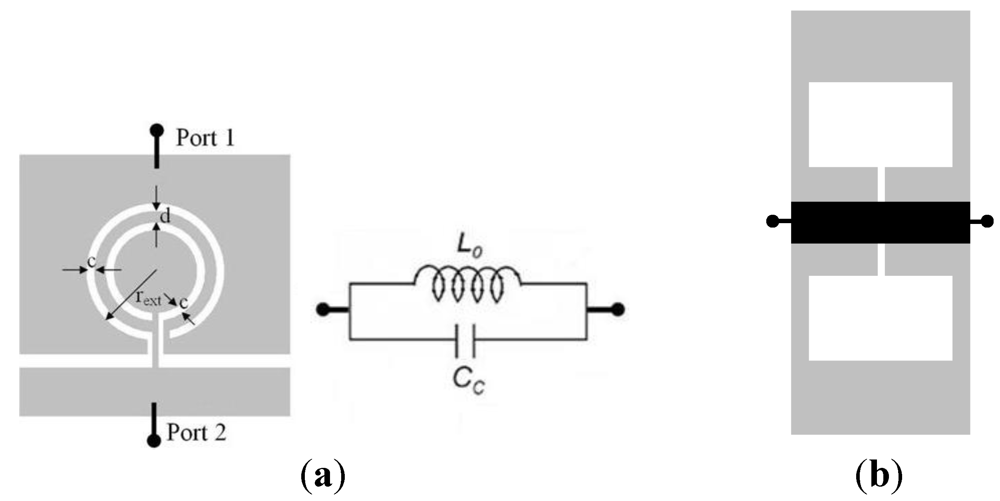
Complementarity can also be applied to the NB-SRR, DS-SRR, 2-SR, SIR and OSRR. Let us consider in certain detail the complementary counterparts of the SIR and OSRR, since they are of special interest for microwave and metamaterial-based circuit design. The complementary version of the open split ring resonator was called open complementary split ring resonator (OCSRR) [
27]. The OCSRR is the complementary (negative) image of the OSRR, but it can also be considered to be the open version of the CSRR. However, the OCSRR must be considered with some caution, since the metallic terminals of the OSRR disappear by applying duality. As shown in
Figure 7(a), the OCSRR is an open particle with terminals for external connection (excitation) as indicated in the figure. From one terminal to the other there are two possible current paths: On one hand, the inductive path through the strip between the ring slots; on the other hand, the capacitive path through the slots. Therefore the OCSRR is an open parallel resonant tank. The capacitance of the particle is the capacitance of the CSRR,
Cc; the inductance is four times larger than the inductance of the CSRR. This means that the OCSRR is smaller than the CSRR by a factor of two. Indeed, the resonance frequency and electrical size of the OSRR and the OCSRR are identical (provided the same dimensions and substrate are considered).
The complementary counterpart of the SIR has been called dumb-bell defected ground structure (DB-DGS). The reason is that this structure is dumb-bell shaped, and it is typically etched in the ground plane of microstrip lines, creating thus a defect, or pattern, in such a ground plane (
Figure 7(b)). This structure behaves like a series connected parallel resonant tank, as reported in [
28]. Thus, OCSRRs and DB-DGSs are of interest in applications where electrically small open parallel resonators are required.
Figure 7.
(a) Open complementary split ring resonator (OCSRR) topology and its equivalent circuit model. (b) Topology of a dumb-bell defected ground structure (DB-DGS) etched in a ground plane of a microstrip transmission line.
Figure 7.
(a) Open complementary split ring resonator (OCSRR) topology and its equivalent circuit model. (b) Topology of a dumb-bell defected ground structure (DB-DGS) etched in a ground plane of a microstrip transmission line.
Many other electrically small planar resonant particles, such as multiconductor SRRs or spirals [
29], Hilbert shaped resonators [
30,
31], electrically tunable resonators [
32,
33]
etc., have been considered in the literature, but are out of the scope of this paper. Nevertheless, the authors recommend the books by Marques, Martín and Sorolla [
7] and by Solymar and Shamonina [
9] for an overview of the resonators considered in this paper and for other electrically small resonant particles.
3.2. Transmission Lines Loaded with Electrically Small Resonators
In microwave applications, rather than isolated, the resonators considered in the previous sub-section are coupled (or connected) to host transmission lines (microstrip lines, CPWs, etc.). Despite the fact that such electrically small particles can also be present in metallic waveguides, the main interest of this paper is planar technology. For this reason, the present section is devoted only to the study of planar transmission lines loaded with semilumped resonators.
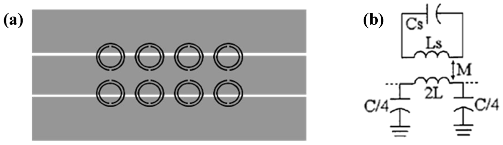
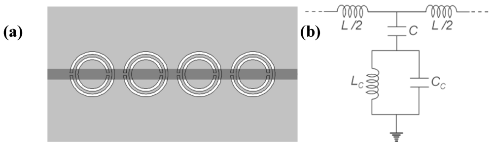
Let us start with the equivalent circuit models of transmission lines loaded with closed resonators. Typically, the SRR (or the 2-SR, NB-SRR, BC-SRR and DS-SRR) are useful particles to load a CPW transmission line. They can also be used by coupling them to a microstrip transmission line, but the corresponding circuit models are not so accurate. The typical topology of a CPW loaded with pairs of SRRs, as well as the lumped element equivalent circuit model of the unit cell, are depicted in
Figure 8 [
34,
35]. The SRRs are etched in the back substrate side, below the slots, so the particles can be excited by the time varying magnetic field generated by the current flowing through the line. The circuit model of the unit cell must take into account the resonator and the line, as well as the coupling between the resonator and the line and, eventually, inter-resonator coupling. In many applications, coupling of the inter-resonator is not required (
i.e., the resonators are separated enough) and can be neglected. This is the case considered here. Nevertheless, the analysis of transmission lines loaded with tightly coupled resonators has been carried out in [
36]. In the circuit model of
Figure 8,
L and
C are the line inductance and capacitance,
Ls and
Cs are the inductance and capacitance of the SRR (or the considered coupled particle), and
M is the mutual coupling between the line and the SRRs. The structure of
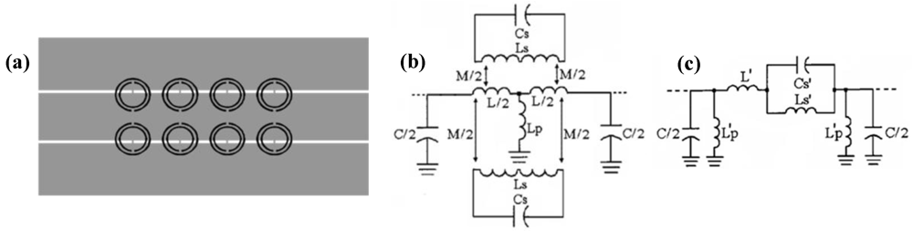
Figure 8 exhibits a stop band behavior that has been interpreted as consequence of the negative effective permeability of the structure (caused by the presence of the SRRs) above resonance, and by the highly positive effective permeability below SRR resonance. To implement a backward wave (or left handed) CPW transmission line, inductive strips between the central strip and the ground planes, above the positions of the SRRs, have been introduced (
Figure 9(a)) [
34,
35]. With the presence of the shunt connected strips, the structure switches its frequency response to a bandpass type response, where wave propagation in the first allowed (narrow) band is backward (typically this structure exhibits a forward wave transmission band at higher frequencies). In this case, the circuit model is that depicted in
Figure 9(b), where
Lp accounts for the pair of shunt connected strips. The circuit model depicted in
Figure 9(b) can be transformed to the circuit depicted in
Figure 9(c) [
35]. The following transformations apply:
Figure 8.
(a) Typical topology of a SRR loaded CPW. (b) Equivalent circuit model of the unit cell. The magnetic wall concept has been applied, so that the model is that of the one half of the structure.
Figure 8.
(a) Typical topology of a SRR loaded CPW. (b) Equivalent circuit model of the unit cell. The magnetic wall concept has been applied, so that the model is that of the one half of the structure.
Figure 9.
(a) Typical topology of a SRR- and strip-loaded CPW. (b) Equivalent circuit model of the unit cell. (c) Transformed circuit model.
Figure 9.
(a) Typical topology of a SRR- and strip-loaded CPW. (b) Equivalent circuit model of the unit cell. (c) Transformed circuit model.
The circuit model of
Figure 9(c) is useful for design purposes since a parameter extractor has been developed [
37], namely, from the electromagnetic simulation (or measurement) of the frequency response of a SRR-loaded CPW, we can easily infer the element values of the circuit model. The technique is very useful but it is out of the scope of this paper. Moreover, from the equivalent circuit model of the unit cell, we can easily predict the bandwidth of the allowed bands, as well as the characteristic impedance of the propagating structures in those bands. The bandwidth can be inferred from the dispersion relation, given by:
with Zs and Zp being the series and shunt impedance, respectively, of the π-model of the considered line (for a T-model, the same expression is also valid). The characteristic impedance of a periodic structure whose unit cell can be described by a π-model is:
and for a T-model, it takes the form:
It has been mentioned before that the electrical size of the SRR can be decreased through different strategies. However, as discussed in [
38], reducing the particle size has the effect of narrowing the bandwidth. Therefore, a trade-off between size and bandwidth when choosing the loading particles must be taken into account. This important aspect is illustrated in
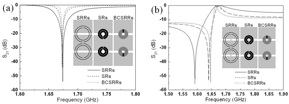
Figure 10, where the transmission coefficient of a CPW transmission line loaded with different resonant elements is depicted. If, for instance, a notch filter with much localized frequency is required, the use of a 2-SR spiral or a BC-2SR, rather than a SRR, is recommended. However, for applications of strip- and resonator-loaded CPW as bandpass filters, SRRs are necessary if the required bandwidth is moderate.
Figure 10.
Layouts and transmission coefficients of several CPWs loaded with pairs of SRRs, BC-SRRs and 2-SRs (
a) and with shunt strips (
b). Relevant dimensions are: Ring width
c = 0.2 mm, distance between the rings
d = 1 mm, external radius
rext = 5.4mm for the SRRs;
c = 0.961 mm,
d = 0.19 mm,
rext = 3.36 mm for the SRs; and
c = 2.12 mm,
d = 0.2 mm,
rext = 3.17 mm for the BCSRRs. For the CPW the central strip width is
WC = 10 mm, the width of the slots is
G = 1.59 mm and the length
D = 12.2 mm. Shunt strip width
wS = 0.2 mm. The considered substrate characteristics are: dielectric constant
εr = 10.2 and thickness
h = 2.54 mm. From [
38]; copyright © 2010, John Wiley & Sons; reprinted with permission.
Let us now consider microstrip lines loaded with CSRRs. The typical topology and circuit model (unit cell) are depicted in
Figure 11 [
25]. The line is described by the inductance
L and by the capacitance
C, which models also the electric coupling between the line and the CSRR, described by the inductance
Lc and the capacitance
Cc. The structure exhibits a stop band behavior that has been interpreted as being due to the negative effective permittivity of the structure in the vicinity of CSRR resonance. A left handed transmission band can be generated by merely cutting gaps in the microstrip line, above the positions of the CSRRs [
26]. In this case the structure is a passband and can be modeled according to the circuit depicted in
Figure 12(b), where the gap is modeled by a π-model consisting of the series capacitance
Cs plus the fringing capacitances
Cf. Such a model can be transformed to the model depicted in
Figure 12(c), with the following transformations [
39]
where
Cpar =
Cf +
CL. Like for the SRR-loaded CPW, CSRR loaded lines can be analyzed through their lumped element equivalent circuit, and expressions (6) and (8). The parameter extraction technique for these CSRR-loaded lines has been published in [
40].
Figure 11.
(a) Typical topology of a CSRR loaded microstrip line. (b) Equivalent circuit model of the unit cell.
Figure 11.
(a) Typical topology of a CSRR loaded microstrip line. (b) Equivalent circuit model of the unit cell.
Figure 12.
(a) Typical topology of a CSRR- and gap-loaded microstrip line. (b) Equivalent circuit model of the unit cell. (c) Transformed circuit model.
Figure 12.
(a) Typical topology of a CSRR- and gap-loaded microstrip line. (b) Equivalent circuit model of the unit cell. (c) Transformed circuit model.
The circuit models depicted in
Figure 11 and
Figure 12 also apply for microstrip lines loaded with complementary spirals or with other complementary closed particles. Concerning the trade-off between particle size and bandwidth, the same comments in reference to SRR-loaded lines also apply (see [
38] for more details and for numerical calculations).
The main relevant limitation of SRR- and CSRR-loaded lines is the narrow bandwidth, which is related to the limited coupling between the line and the resonator. In band pass structures, moderate and wide bands have been achieved by merging the backward and the forward wave transmission bands [
41]. However, the validity of the models of the SRR- and CSRR-loaded lines in the forward wave transmission band is restricted to only a small portion of the band [
42]. The DS-SRR (or DS-CSRR) has been considered in order to implement moderate or even wideband stop band structures, but this particle is electrically larger than the SRR (or CSRR), and therefore the accuracy of the circuit model to properly describe lines loaded with such particles is questionable. An alternative approach to implement wide band structures is the combined use of OSRRs and OCSRR in transmission lines.
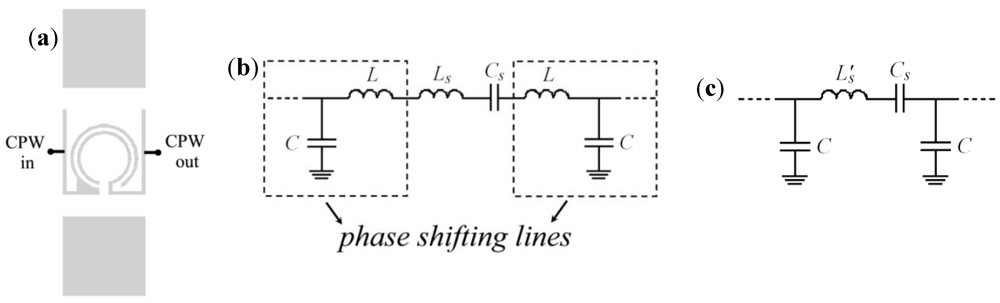
Let us consider a CPW loaded with an OSRR (
Figure 13(a)). The circuit model of this structure is not merely a series resonator between the input and output ports of the CPW. As discussed in [
43], the line introduces some phase shift that must be taken into account for an accurate modeling. Such phase shift can be accounted for by cascading phase shifting lines to the series resonator,
Ls-
Cs, modeling the OSRR. In practice, such shifting lines can be modeled by means of a lumped capacitance
C and inductance
L, and the circuit model is that shown in
Figure 13(b), which in turn can be simplified to the model depicted in
Figure 13(c). For OCSRR loaded lines (
Figure 14), a similar phenomenology applies. That is, the structure cannot be simply modeled by means of a shunt connected parallel resonator. A certain phase shift appears, and the equivalent circuit model is that depicted in
Figure 14(b,c). In the models of
Figure 13 and
Figure 14,
L and
C must be considered parasitic elements. The frequency response of CPW transmission lines loaded with either OSRRs or OCSRRs reveals that the structures exhibit a band pass behavior with very wide transmission bands. As will be shown in the next section, by cascading OSRR and OCSRR-loaded CPWs, it is possible to implement transmission lines with composite backward and forward characteristics, as well as wide band filters. As compared to other structures based on closed rings, the main advantage of these OSRR and OCSRR based lines, is that the equivalent circuit of the structures models their behavior to a very good approximation within the whole transmission band.
Figure 13.
Layout (a), circuit model (b) and simplified circuit model (c) of a CPW transmission line loaded with a series connected open split ring resonator (L’s = Ls + 2L).
Figure 13.
Layout (a), circuit model (b) and simplified circuit model (c) of a CPW transmission line loaded with a series connected open split ring resonator (L’s = Ls + 2L).
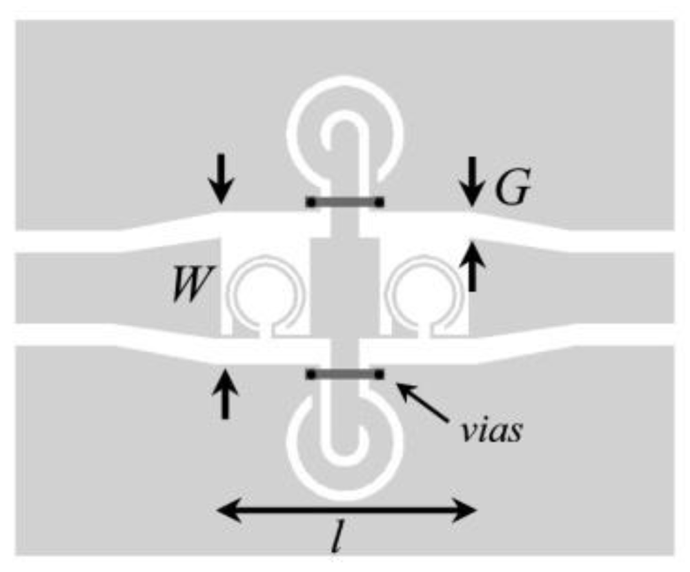
Figure 14.
Layout (a), circuit model (b) and simplified circuit model (c) of a CPW transmission line loaded with a pair of open complementary split ring resonators, where C’p = 2Cp + 2C and L’p = Lp/2. The backside strips (in dark grey) connecting the different ground plane regions are necessary to prevent the slot mode of the CPW and the second resonance of the open complementary split ring resonators.
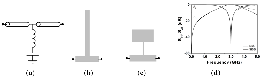
To end this section, we will consider the SIRs coupled to transmission lines. These resonators are useful to implement shunt connected series resonators. In microstrip technology, the SISS topology of
Figure 1(c), where the SISS is merely modeled as a series grounded resonator, is very useful (the limitations of this model are discussed in [
11]). In CPW technology, SIRs are typically implemented by backside etching the wide SIR strip sections below the central strip and ground planes of the CPW structure, as shown in
Figure 15. The equivalent circuit model of the SIR-loaded CPW is also depicted in
Figure 15.
L and
C are the line inductance and capacitance, whereas the SIR is modeled by
Ls and
Cs.
Figure 15.
Typical layout of a SIR-loaded CPW (a) and equivalent circuit model (b).
Figure 15.
Typical layout of a SIR-loaded CPW (a) and equivalent circuit model (b).


