Article

A Portable Optical Sensor for Microplastic Detection: Development and Calibration

by
Maximiliano Campos-López
1,
Ricardo Aguilar-Garay
1,
Dafne E. González-Rodriguez
1,
Verónica I. Mejía-Lopez
1,
Margoth M. Gamboa-Lugo
2,
Vicente Garibay-Febles
3,*,
Marco A. Reyes-Guzmán
4,
Álvaro Gordillo-Sol
4 and
Jorge A. Mendoza-Pérez
1,*
1
Laboratory of Clean Technologies, Development of Environmental Processes and Green Engineering, Escuela Nacional de Ciencias Biológicas, Instituto Politécnico Nacional, Mexico City 07320, Mexico
2
Faculty of Chemical-Biological Sciences, Autonomous University of Sinaloa, Av. Las Américas S/N, Culiacán 80000, Sinaloa, Mexico
3
Instituto Mexicano del Petróleo, Eje Central Lázaro Cárdenas Norte 152, Gustavo A. Madero, Mexico City 07730, Mexico
4
Basic Sciences Academy, Unidad Profesional Interdisciplinaria en Ingeniería y Tecnologías Avanzadas, Instituto Politécnico Nacional, Avenida Instituto Politécnico Nacional 2580, La Laguna Ticomán, Gustavo A. Madero, Mexico City 07340, Mexico
*
Authors to whom correspondence should be addressed.
Appl. Sci. 2025, 15(9), 4757; https://doi.org/10.3390/app15094757
Submission received: 15 March 2025 / Revised: 12 April 2025 / Accepted: 15 April 2025 / Published: 25 April 2025
(This article belongs to the Section Optics and Lasers)

Abstract

:
Microplastics are ubiquitous in the environment and represent a serious risk to ecosystems and human health. This study describes a prototype sensor designed to detect microplastics by analyzing samples with multiple wavelengths of light. The system uses samples of commercially available microplastics and includes passive low-pass filters to reduce noise for accurate readings. The prototype measures light attenuation and produces color spectra that helps identify microplastics. Its design focuses on precision, electronic control, and optical sensing, making it an affordable option for environmental monitoring. Early experiments demonstrate that the prototype is sensitive and reliable under a variety of conditions. Future improvements may add machine learning and fuzzy logic to increase accuracy and expand its use.

1. Introduction

Pollution caused by human activities has severely damaged ecosystems and public health. Microplastics (MPs) are among the most concerning pollutants, and their long-term effects are still uncertain. The term “microplastics” was first used in 2004 to describe plastic particles smaller than 5 mm. However, the scientific community has yet to agree on a clear definition. Understanding their long-term effects is becoming increasingly important [1].
Since 1950, global plastic production has skyrocketed, reaching a total of 8.3 billion metric tons [2]. Microplastics pollute the oceans, with industries releasing approximately 1.3 million metric tons of microplastics annually from sources such as tire dust, plastic pellets, textiles, and personal care products. Projections indicate that this figure will rise to 3 million metric tons by 2040. The fishing and tourism industries suffer massive economic losses, incurring costs of between USD 500 billion and USD 2.5 trillion annually due to this pollution [3].
Microplastics (MPs) disrupt aquatic ecosystems when crustaceans and mollusks consume them, resulting in damage to their digestive, reproductive, and immune systems [4]. The impact of microplastics extends up the food chain, accumulating in key food sources, including seafood, milk, honey, and beverages. Ingesting these particles may cause toxic, allergenic, and inflammatory reactions, as well as intestinal blockages, reduced mucus secretion, intestinal barrier damage, gut microbiota imbalance, and altered metabolism [5].
Bioplastics, such as polylactic acid (PLA), are gaining popularity for their biodegradability and renewable origins. However, under specific conditions, they can fragment into microplastics, thereby exacerbating pollution. Synani et al. analyze the environmental consequences of PLA production and call for vigilant monitoring of its degradation products [6]. Nampoothiri et al. (2020) urge scientists to thoroughly evaluate the environmental footprint of PLA and its breakdown products [7].
Fourier-transform infrared spectroscopy (FTIR) and Raman spectroscopy (RMS) are the dominant primary techniques for identifying microplastics. These methods determine the polymeric composition of microplastics in water-based environments, thereby enhancing our understanding of their prevalence and impact on aquatic ecosystems [8,9,10]. FTIR identifies polymer composition by studying how light interacts with matter, but RMS detects particles as small as 1 micron and provides detailed morphological and chemical analysis. RMS is particularly effective for compounds with aliphatic, aromatic, or carbon–carbon double bonds. To ensure accurate Raman spectra and avoid fluorescence interference, it is important to purify samples [11].
Although these methods prove effective, they require sample purification to avoid interference and are not always portable or cost-efficient for large-scale monitoring [12,13,14].
RMS is especially valuable for detecting MPs in diverse matrices, including human samples, as demonstrated by Xu et al. [15], for the identification of microplastics in water bodies. They demonstrated its capability to detect particles as small as 1 µm and provide detailed morphological and chemical analysis. Similarly, Prata et al. [16] highlighted its effectiveness in detecting MPs in human tissue samples, highlighting its potential for studying the impact of microplastics on human health. Despite its high accuracy, Raman spectroscopy’s limitations include its susceptibility to fluorescence interference and the need for extensive sample preparation.
FTIR, on the other hand, has been widely used for polymer identification and analysis of contamination. For example, the work by Zea Cobos et al. [17], which developed standardized FTIR methodologies to detect microplastics in drinking water, employed cellulose nitrate filters and Nile red staining to enhance accuracy.
Willans et al. [18] effectively used reflectance–FTIR spectroscopic imaging to detect polyethylene and polypropylene microplastics in marine salt samples, demonstrating its potential for high-throughput environmental monitoring. However, FTIR encounters limitations, including difficulty in detecting particles below a specific size threshold and dependence on controlled laboratory settings.
Furthermore, alternative techniques to FTIR and Raman spectroscopy are needed to determine the presence of microplastics in aquatic ecosystems [19].
Researchers actively develop alternative techniques to overcome the limitations of traditional methods for detecting microplastics. Biomonitoring methods, such as using aquatic mosses like Fontinalis antipyretica, have the potential to identify MPs and mesoplastics in freshwater ecosystems. Single-molecule tools also enable precise detection and quantification of microplastics across various environments.
In 2022, V. Carrieri and Z. Varela investigated the use of Fontinalis antipyretica as a biomonitor for MPs and mesoplastics. They compared how native moss samples and moss clones retained fluorescent polystyrene particles under laboratory conditions and in field settings near wastewater treatment plants [20].
Recent advances in single-molecule tools, such as atomic force microscopy (AFM), provide a more detailed understanding of the physicochemical properties of aquatic microorganisms at the nanoscale, thereby aiding biodiversity preservation and ecosystem understanding [21]. Additionally, membrane filters that support the samples should not introduce background interference during spectrum acquisition [8,22]. Despite their potential, these methods also face challenges in scalability and integration into fieldwork.
The ability to detect and quantify microplastics is imperative for effective environmental management. Conventional methods, such as density separation, filtration, and visual sorting, have proven to be effective. However, they are often time-consuming, underscoring the necessity for more expeditious approaches.
The proposed prototype offers researchers a practical way to detect microplastics and confirm their presence in samples. It provides a preliminary analysis by measuring light attenuation and generating color spectra to help researchers identify contaminated samples. This approach simplifies sample processing and ensures that only relevant samples are sent for advanced techniques, such as Raman spectroscopy. As a result, it saves time and reduces costs while improving resource allocation.
The findings presented in this paper offer a comprehensive description of the device’s design, calibration, and methodology. Additionally, the paper discusses the prototype’s performance during beta testing with commercial microplastics, highlighting its sensitivity and reliability.

2. Materials and Methods

The development of the prototype was focused on the accurate detection of microplastics. Among the prevalent materials, such as acrylonitrile butadiene styrene (ABS), polylactic acid (PLA), and polyethylene terephthalate (PET), PLA was selected due to its accessibility and common use. Sensors and test probes were designed specifically to analyze this material.
Testing was conducted in a controlled environment using commercially available microplastics, with PLA serving as the standard for comparison with organic materials. Utilizing a light source, the sensor measured the transmitted intensity in volts. The test quantified optical properties through a process known as “experimental absorbance” or “attenuation”. Rectangular samples measuring 10 × 3 cm were meticulously placed on glass slides for analysis.
To improve efficiency, a scanning mechanism inspired by a 2-axis Cartesian CNC system (X and Y axes) was implemented. We powered the prototype with a Raspberry Pi 4 and controlled it using two stepper motors with A4988 drivers (Allegro MicroSystems, Manchester, NH, USA). The graphical user interface (GUI) provided two modes: microscopy and LED. The equation for measuring absorbance is given by:
A = log I t I 0
Equation (1) is the logarithmic absorbance equation, and it calculates absorbance ( A ) based on the ratio of transmitted ( I t ) to initial ( I 0 ) light intensities. This is where ( I t , I 0 ) are the transmitted light intensity, and the incident light intensity, respectively. This equation allows for the determination of the sample’s optical attenuation, which serves as a proxy for microplastic detection.
In microscopy mode, the system takes images of the samples and uses algorithms to detect microplastics. In LED mode, the user selects a wavelength to irradiate the sample and obtains its attenuation value, which provides an initial indication of microplastics (MPs). The user can then employ the microscopy mode to confirm these findings and, with a more robust probe, ensure accurate detection. A 7-inch screen connected to the Raspberry Pi 4 displays the results, which can also be sent wirelessly to a computer.
We covered the mechanism with a black cloth to block noise and improve calibration. This approach reduced interference from ambient light. Additionally, a printed circuit board (PCB) was designed to interconnect all the circuits for sample detection and light emission. This design compacted the prototype and eliminated noise from the DuPont cables. Prior to the initiation of production, rigorous PCB simulations were conducted to identify and rectify any potential issues. Subsequent to this, we proceeded with the assembly of all of the components necessary to construct the final probes.
The following sections describe the prototype components, explain their functions, and highlight the design considerations behind their development. This section will focus on polylactic acid (PLA), a prevalent microplastic found in rivers and lakes. It is frequently found in water and soft drink bottles. As a widely used biodegradable bioplastic in many products, PLA is important in environmental studies [6,23].
Microplastics absorb visible-wavelength light while reflecting very little, unlike organic waste, which mostly reflects visible light and absorbs little. This difference is clear in absorption spectrophotometry (transmittance), their reflective properties, and the reflectance of other components [24,25,26,27]. To match these characteristics, we chose light sources with wavelengths between 360 nm and 960 nm. The specific wavelengths included 370, 385, 395, 405, 456, 470, 525, 570, 590, 605, 625, 636, 840, and 940 nm.
We have created a sampling method based on the range and spectrum of microplastics to work with materials that fit the system. The system has been engineered to detect a variety of materials. However, it requires calibration to identify the spectrum of the target material. Initial testing focused on PLA due to its prominence in the relevant literature. The sensor quantifies the degree of light absorption or transmission by the sample, utilizing a process known as “absorbance measurement”. This parameter helps differentiate microplastic particles from organic matter.
We map the detected intensity I d e t e c t e d on a scale of 0 to 3.3 volts, with 3.3 volts indicating sensor saturation. We express the relationship between the incident intensity ( I 0 ) and the transmitted intensity ( I t ) through the sample as follows:
I d e t e c t e d = 3.3 I t I 0
Equation (2) is the detected intensity equation. This equation determines the detected light intensity ( I D e t e c t e d ) as a scaled factor of the transmitted light intensity ( I t ) relative to the initial intensity ( I 0 ).
Because I d e t e c t e d corresponds to the voltage output proportional to the sample’s optical properties, this equation reflects the linear scaling of the photodiode output to the maximum measurable voltage (3.3 V). Samples that show lower transmitted intensities yield proportionally lower output voltages, which facilitates the differentiation between microplastic particles and other materials.
The first step in the process is to use gloves and a clean work area to avoid contamination, followed by collecting the sample (PLA) and measuring its attenuation. Subsequent to the measurement of attenuation, the samples are examined under a microscope to identify the microplastics and discard the non-plastic debris. Moreover, we used digital image processing (DIP) to classify the microplastics based on their shapes.
Despite the fact that this article focuses on LED-based detection, we did not perform a detailed microscopic analysis, but preliminary tests based on morphological characteristics will be explained in the next article [28]. And we discussed it in the “Microscopy and Image Processing Results” section.
Finally, we send the samples for spectroscopic analysis to determine their composition. This method ensures that the samples are relevant and reliable, providing accurate data for evaluating microplastic contamination [29,30].
In the future, “Phase 2” research could focus on sampling the environment and identifying sites with significant microplastic accumulation. The selection of an appropriate sampling method will be decided according to the needs of the study, e.g., net sampling for water column analysis, bulk sampling for volumetric concentration, continuous plankton recorder for plankton-associated microplastics, or direct in situ filtration for immediate processing.

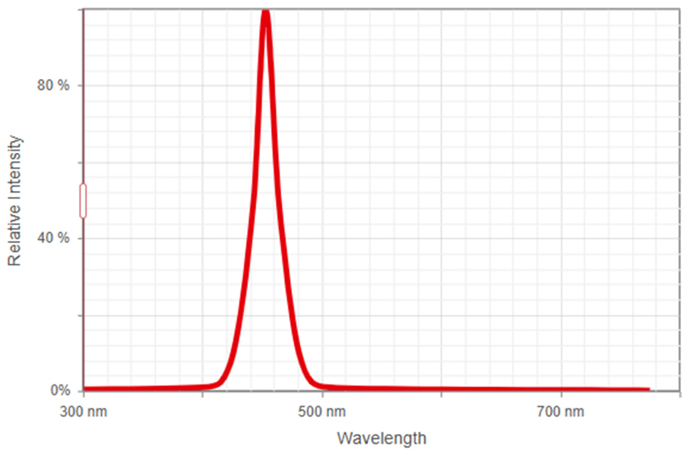
2.1. Wavelength Selection

The proposed LEDs are to be evaluated based on the following criteria, as determined by their detection range:
  • Select a light source that emits a range of wavelengths suitable for interacting with the microplastics to be detected. Factors such as power, stability, divergence, and cost must be considered for effective interaction with microplastics;
  • Design an optical system to focus and direct a light beam to the area of interest, allowing collection and analysis of the optical signal reflected or transmitted by microplastics.
The prototype utilizes light-emitting diodes (LEDs) and a servomotor to modulate the wavelengths, ranging from ultraviolet to infrared. We aimed for high precision, so we sourced LEDs with specific wavelength characteristics. We purchased the LEDs from Würth Elektronik [31], specifically from the WL-SMTW SMT Mono-color TOP LED Water clear family. Figure 1 shows the wavelength spectrum for the Blue 456 color of these LEDs. We selected the LEDs for surface-mount soldering on a manufactured PCB, achieving precise control over the emitted light spectrum.
We obtain the sample’s attenuation value using a photodiode, allowing researchers to distinguish between PLA and other materials. This methodology is pivotal for analyzing the optical properties of materials and makes a significant contribution to the field of spectroscopy [32].

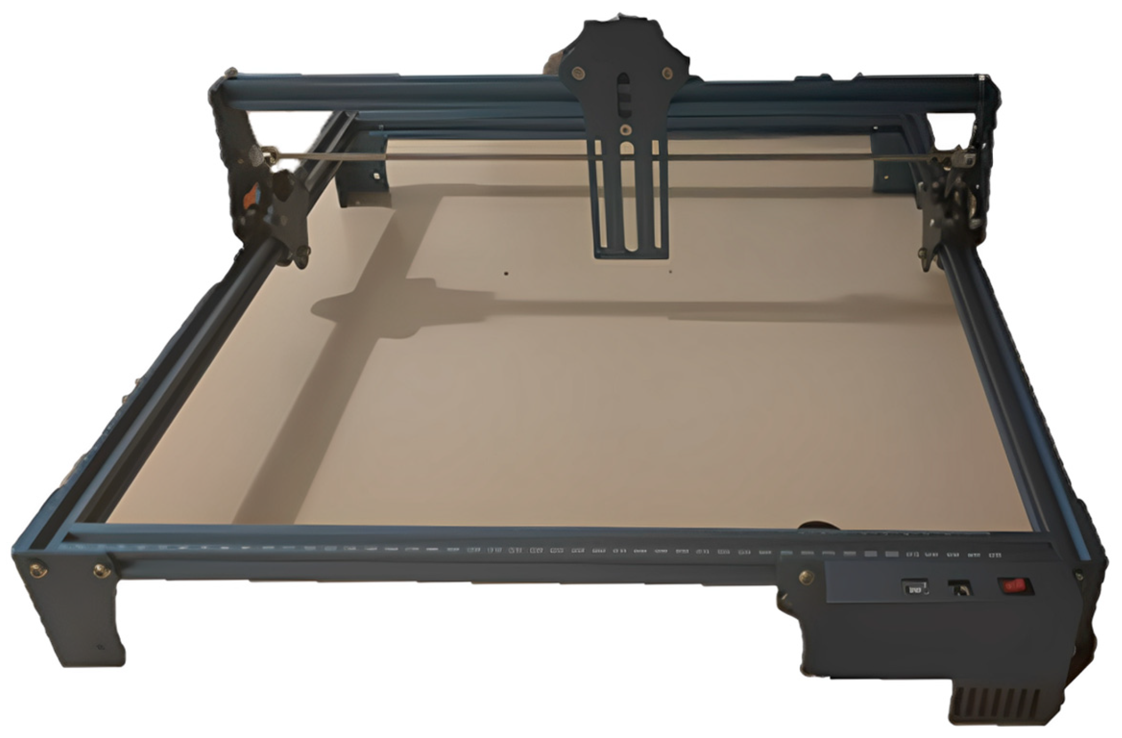
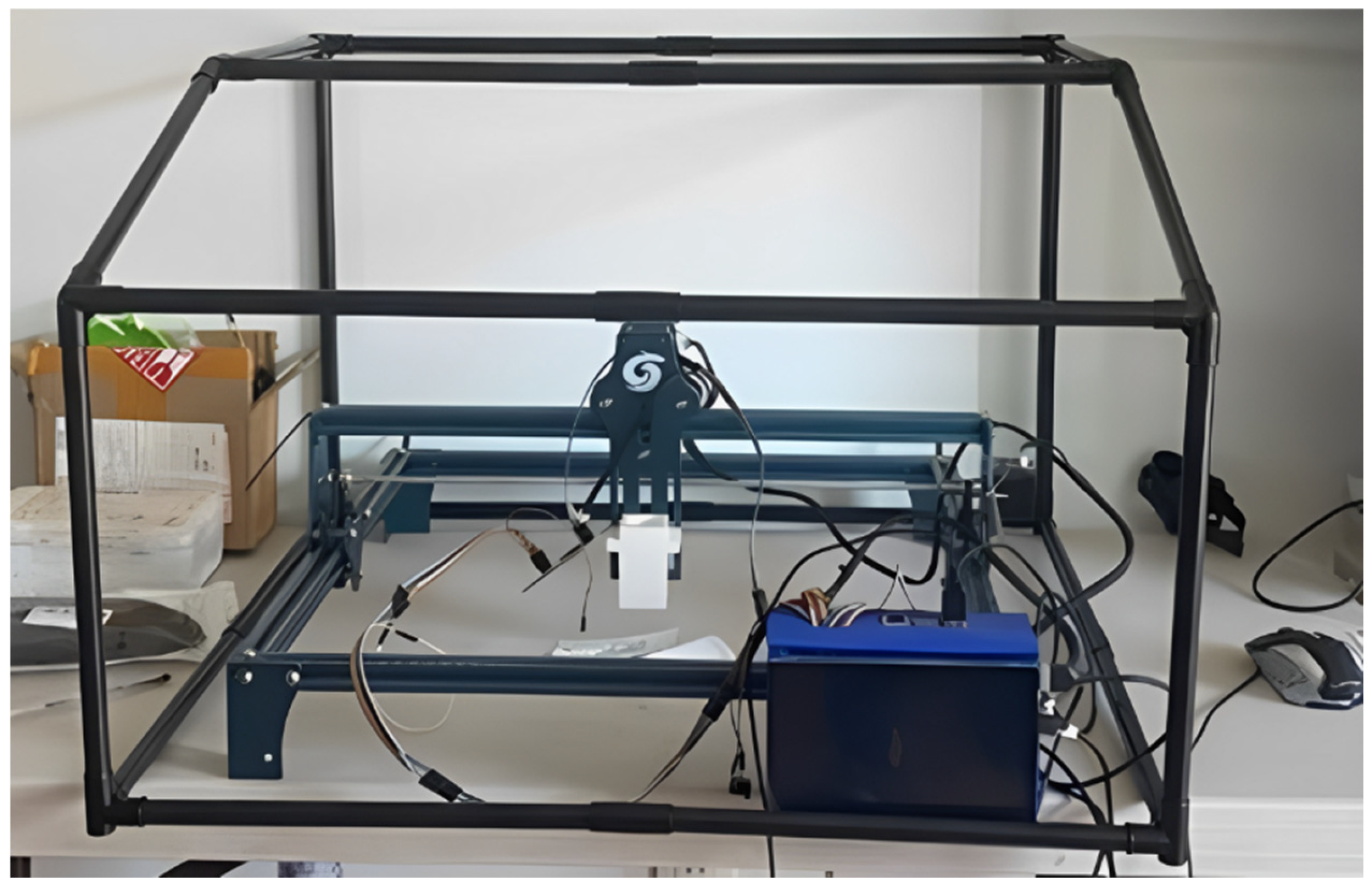
2.2. Four-Bar Structure

The sample facilitated the optimization of the manufacturing workspace for the prototype. The objective of the prototype is to augment the area and analyze multiple samples. We proposed the dimensions and characteristics as follows: 45 cm × 45 cm. By leveraging Cartesian movement across two axes of a CNC (X, Y) with a four-bar structure, we enable controlled motion in both axes, facilitating surface mapping and sensor measurement acquisition. Figure 2 shows the structure. We used an old laser cutter from Sulpfun for the prototype, and we used SolidWorks version 2022 [33] to simulate the structure and design additional components. The control of this structure is facilitated by two stepper motors interfaced with an A4988 driver.

2.3. Raspberry Pi 4 (8GB RAM) and A4988 Driver

A Raspberry Pi is a series of single-board computers developed by the Raspberry Pi Foundation [34].
This study employed a Raspberry Pi 4 with 8GB of RAM to control the prototype. The Raspberry Pi 4’s features of low cost and power efficiency make it ideal for IoT devices and prototypes, and its GPIO capabilities enhance functionality. The Raspberry Pi functions as the central processor. The system incorporates a demultiplexer and a digital-to-analog converter, enabling it to interpret external signals from the LED.
The GPIO pins were utilized to control the driver, which allows for axis movement via NEMA 17 stepper motors (Applied Motion Products, Morgan Hill, CA, USA) and an A4988 driver. This configuration ensures precise step motor control and accurate surface mapping. The schematic connections and the A4988 control library are illustrated in Figure 3 and Table 1, respectively. Figure 4 presents a flow chart of the programming code.
Wiring Connections
The A4988 driver was connected to the GPIO pins of the Raspberry Pi in the following manner:
  • The A4988’s step pin was connected to a Raspberry Pi’s GPIO pin to control the stepping;
  • The A4988’s direction pin was connected to a Raspberry Pi’s GPIO pin to manage the rotation direction;
  • The A4988’s MS1, MS2, and MS3 pins were attached to the Raspberry Pi’s GPIO pins to select the micro-stepping mode, if necessary;
  • The A4988’s VMOT pin was connected to an external power supply, which should be between 8 V and 35 V, to power the motor;
  • The ground pin of the A4988 was connected to the ground on the Raspberry Pi;
  • The A4988’s 1A, 1B, 2A, and 2B pins were connected to the motor’s corresponding coils (NEMA17 motor wires).
Setting Current Limit
  • Adjust the current limit using the potentiometer ( V r e f ) on the A4988;
  • Measure V r e f using a voltmeter and set it according to your motor’s specifications.

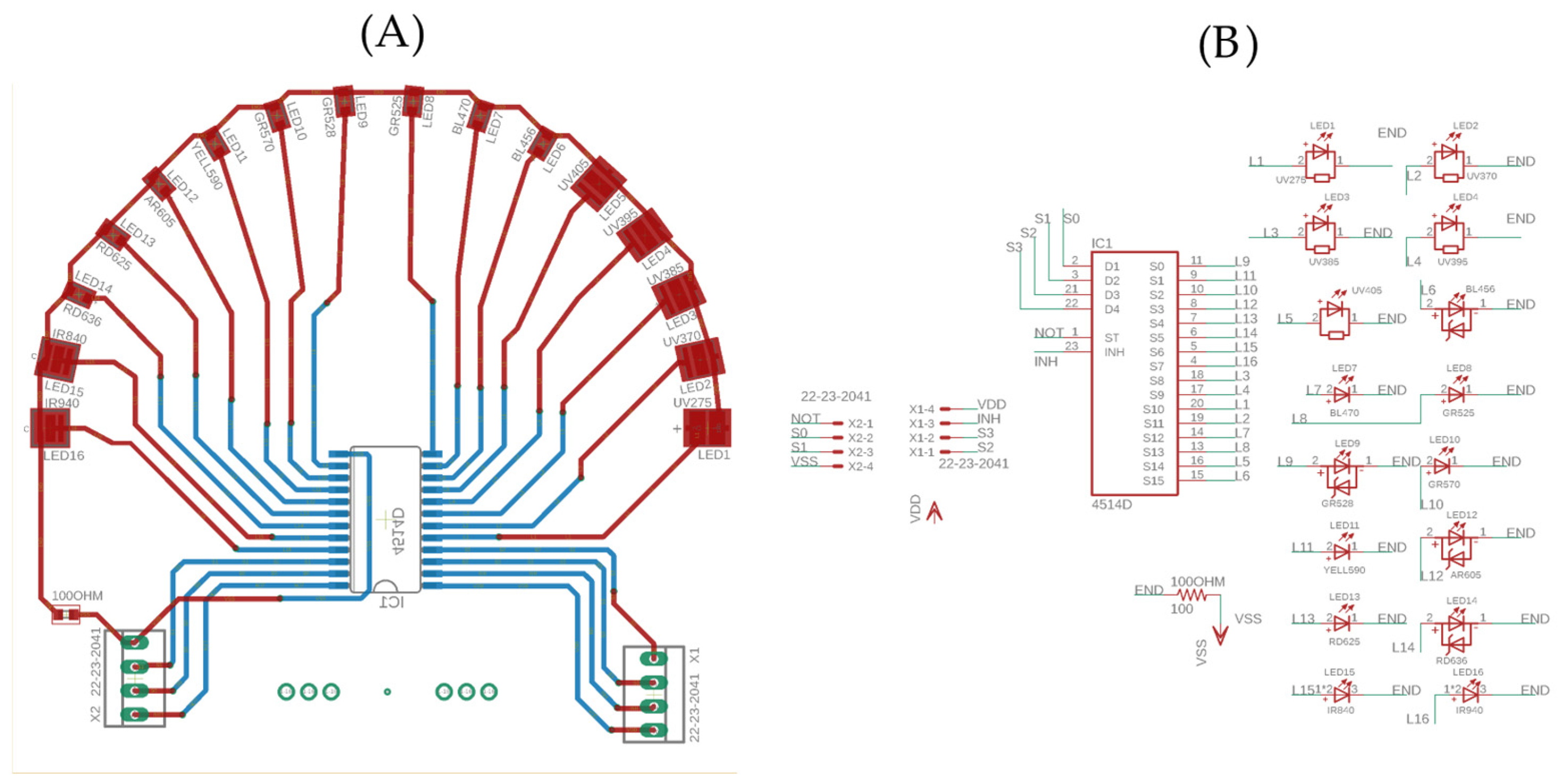
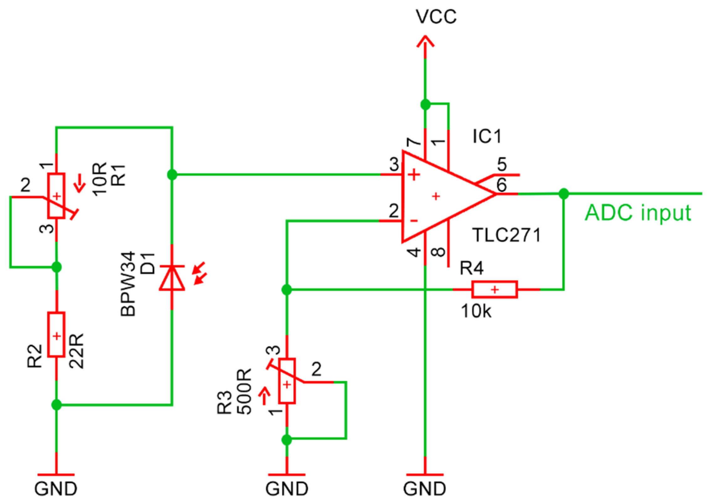
2.4. Printed Circuit Board (PCB) for Wavelength Control

The Y-axis movement of the structure contains a double-sided custom-designed printed circuit board (PCB) that manages different wavelengths. The PCB was designed using EAGLE [35] and comprises the following circuits:
  • Multiplexer: the CD4114D multiplexer facilitates switching between different wavelengths;
  • Analog-to-digital converter (ADC) circuit: the MCP3202 ensures high-resolution signal transduction with its 12-bit bandwidth rate for accurate measurements.
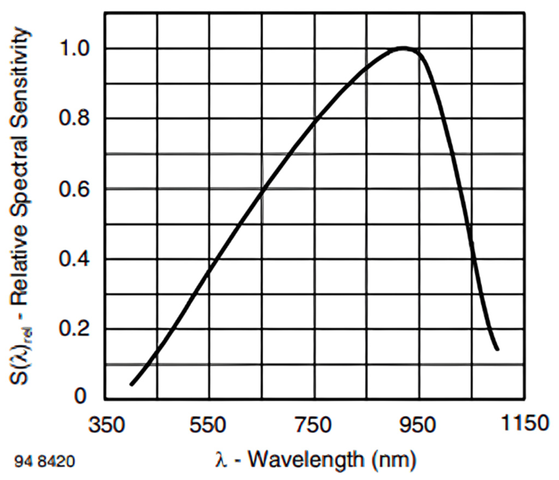
Due to manufacturing time constraints, the PCB was outsourced to a company specializing in rapid prototyping. The assembly process included mounting the mentioned circuit components and the sixteen different LEDs. The 66 mm × 62.7 mm double-sided design was implemented to prevent fragile and excessively long tracks that could generate parasitic resistance. The board was manufactured by JLCPCB (Shenzhen JIALICHUANG Electronic Technology Development Co., Ltd., Shenzhen, China) [36]. All are shown in Figure 5.

2.5. Detector BP34W

In the selection of the photodiode, the primary consideration was the detection range, given the implementation of various LEDs ranging from ultraviolet (UV) to near infrared. We decided to use the BP34W, which has a detection range spanning from 300 nm to 1100 nm. When the sample is exposed to the light source, the BP34W detects the transmitted light from the microplastic. Consequently, the photodiode generates an electrical signal proportional to the intensity of the detected light, thereby providing the attenuation value [37]. Figure 6 shows the relative spectral sensitivity of the BP34W, as provided in the manufacturer’s datasheet by Vishay [38]. Subsequently, an operational amplifier converts the photodiode current into a voltage signal that can be readily interpreted. Finally, the system maps this amplified voltage to the attenuation scale, allowing microplastics to be differentiated based on their optical properties.
The relationship between the optical power ( P o p t ) of the detected light and the output current ( I p h o t o ) of the photodiode is expressed as:
I p h o t o = R λ P o p t
Equation (3) is the photodetector output equation.
where:
  • I p h o t o is the output current generated by the photodiode;
  • R λ is the responsivity of the photodiode at the wavelength of the incident light (units: amperes per watt);
  • P o p t is the optical power of the transmitted light detected by the photodiode (units: watts).
To enhance the performance of the BPW34 photodiode mentioned, the TLC27L2BCD operational amplifier was utilized. The following section will elucidate the alterations made to the operational amplifier. The modification entailed the implementation of a positive gain configuration. Specifically, the configuration of a non-inverting amplifier was implemented, resulting in a gain of 1,000,000. This methodology aligns with the approach outlined by authors Richard Slávik and Miroslav Čekon in their article [39].
We used the circuit illustrated in Figure 7. In the article, they used the TLC271. One reason for this is the supply voltage range, as it supports a supply voltage range of 3 V to 16 V, providing flexibility for various applications.
The gain of the non-inverting amplifier is calculated using the following formula:
A v 1 + R f R 1
Equation (4) is the low-pass filter equation.
where:
  • A v : amplifier gain, representing the ratio between the output signal and the input signal;
  • R f : feedback resistance connected between the output and the negative input terminal of the operational amplifier;
  • R 1 : resistance connected between the negative input terminal and the ground.
TLC271 is characterized by its high input impedance, which mitigates the loading effect on the preceding stage and ensures precise signal amplification. This characteristic allowed us to maintain signal integrity while enhancing the performance of our prototype. For our application, we used the TLC27L2BCD operational amplifier (TME Group, Łódź, Poland) instead of the TCL271, which is ideal for applications requiring multiple Op-Amps (operational amplifiers) in a single package, and due to its superior slew rate. The higher slew rate facilitates expeditious signal processing, a prerequisite for attaining the precision and expediency demanded in our work.
Filters are of great importance in circuit design because they reduce interference from external sources and ensure a clear, undistorted signal. We implemented a passive low-pass filter to mitigate the noise caused by motor vibrations and external interference that affected the output. This filter effectively minimizes the undesired frequencies and preserves signal clarity. We placed the low-pass filter at the front of the amplification stage (Figure 8), which optimizes performance by targeting the noise before the signal enters the amplification process. We chose an RC filter that separates frequencies, allowing certain desired signals to pass. Its simplicity and the RC network’s recognition as the simplest form of a low-pass filter make it a good choice. The RC formula is given by Equation (5).
F c = 1 2 π R C
Equation (5) is the low-pass filter equation.
Utilizing the property of low-pass circuits to filter signals below 100 kHz, we prevent signals above this frequency from reaching the photodiode, effectively cutting very high frequencies that generate noise [40].
Raspberry Pi 4 was used for a graphical user interface (GUI). This interface is key to the system’s operation, functioning as a dedicated application for user interaction and prototype management. It is essential to the system’s architecture to manage the real-time multiplexing wavelengths and the motors. This configuration improves the user experience and enhances the prototype’s mechanical movements. The application’s execution on the device enables touchscreen interaction with the detection platform, improving accessibility. The prototype’s design, intended for use in professional environments and by laboratory personnel, is supported by the GUI’s facilitation of user interaction, as illustrated in Figure 9.
In order to develop the GUI, the following criteria were used, based on experience with microplastics, the specific needs, and the intended purpose of the prototype.
The user interface (UI) design basics are the following:
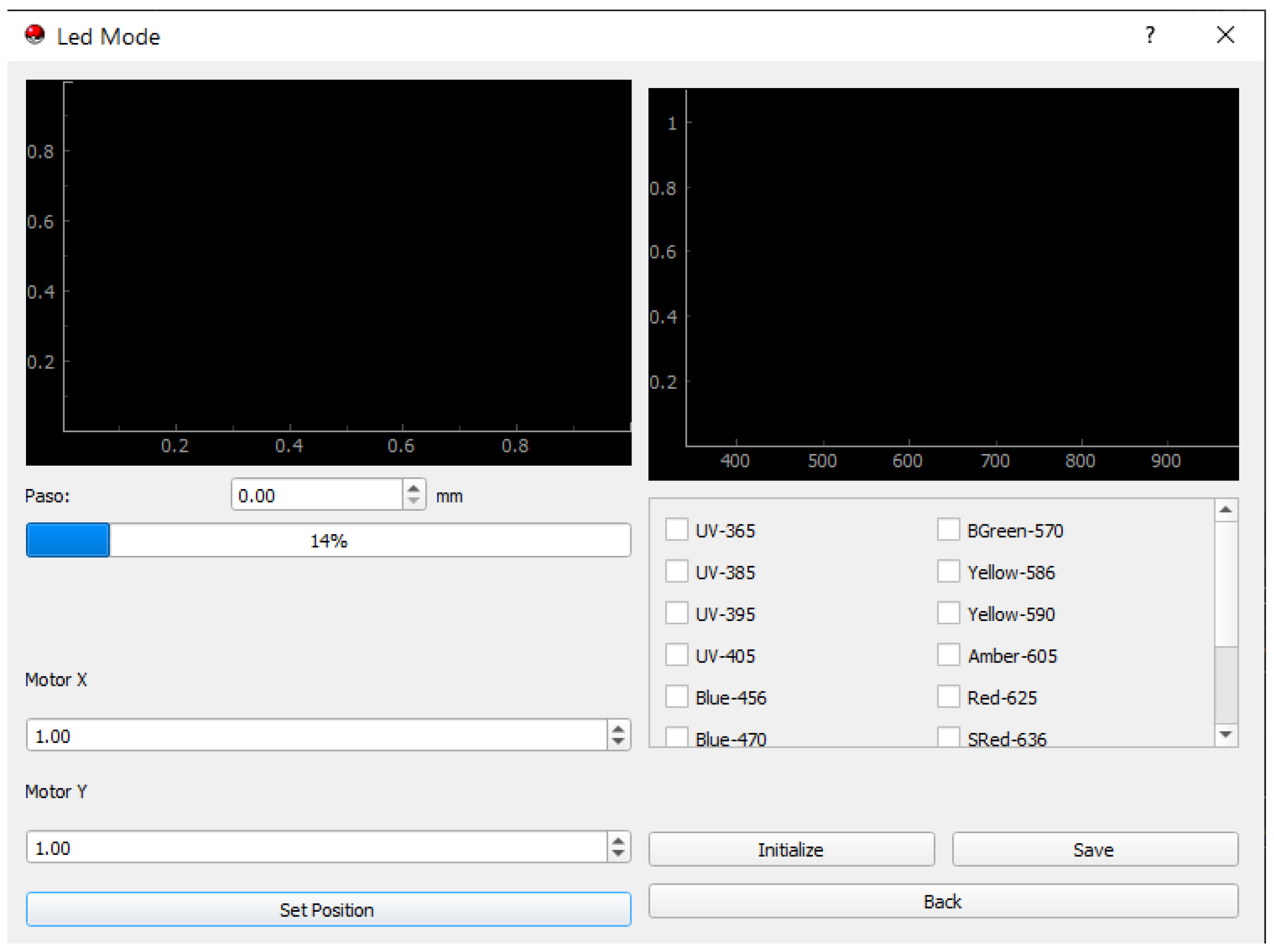
  • Definition: user interface design focuses on anticipating what users need to do;
  • Purpose: UI software bridges the gap between users and the underlying functionality of a system;
  • Importance:
    o
    Usability: a well-designed UI enhances usability, making it easier for users to achieve their goals efficiently;
    o
    Productivity: intuitive interfaces reduce learning curves and increase productivity;
    o
    Aesthetics: a visually appealing UI creates a positive impression and encourages user engagement;
    o
    Consistency: the UI comprises several screens and components to ensure a cohesive experience;
    o
    Accessibility: thoughtful UI design accommodates diverse user needs, including those with disabilities;
  • Methods and techniques:
    o
    Interaction design: defining how users interact with elements (such as buttons, forms, and menus) and ensuring smooth transitions;
    o
    Visual design: designing the look and feel, including colors, typography, and layout;
    o
    Information architecture: organizing content in a logical manner for easy navigation;
    o
    User research: understanding user needs, preferences, and pain points;
    o
    Prototyping: creating interactive mockups to evaluate and iterate on design concepts;
    o
    User testing: gathering feedback from real users to refine the UI [41,42].
The complete structure of the developed GUI user interface is shown in Figure 10, Figure 11 and Figure 12.

3. Results and Discussion

We used commercially purchased microplastics for this study to ensure consistency and reliability. The microplastics were analyzed directly on a glass slide, thereby demonstrating the versatility of the method and the optical sensor’s capacity to detect microplastics under various conditions without the need for a special collection process.
Three stages of evaluation were used to ensure accuracy. Initially, the system was tested in an uncontrolled environment to evaluate its adaptability to external factors. Second, laboratory testing was conducted under controlled conditions to assess baseline performance and identify issues. Finally, we test the sensor in a controlled environment and assess its robustness and stability in real-world conditions.
The prototype systematically scans each sample, acquiring 2000 data points per LED, with a total testing time of 20 s. This balanced approach ensures optimal resolution and efficiency. While augmenting the number of data points enhances resolution, it also extends operating time. Once collected, the data is stored in CSV format for later analysis with various software tools.
The system supports partial automation, enabling users to configure and run multiple samples with different settings. The GUI facilitates user interaction by allowing users to select specific parameters and LEDs. However, the process is not fully automated, as manual intervention is required to select particular parameters and LEDs. Future developments aim to enhance the system’s automation capabilities, making it more user-friendly and efficient for large-scale applications.
Overall, the meticulous testing process and careful design of the sensor ensure its reliability and accuracy in detecting microplastics, making it a valuable tool for environmental monitoring and research.
The following protocol must be followed to operate the sensor:
  • Personal protective equipment (PPE): wear clean lab coats, gloves, and safety goggles;
  • Disinfect work surfaces: wipe down all work surfaces, including benches, tables, and equipment, with a disinfectant solution (e.g., 70% isopropyl alcohol or a bleach solution);
  • Microplastic-handling tools: clean tools (tweezers, scissors, etc.) by rinsing them with distilled water and wiping them with a lint-free cloth soaked in a disinfectant solution;
  • Control samples: Use control samples or blanks to verify the absence of external contamination. Handle these samples with care to avoid introducing contaminants.

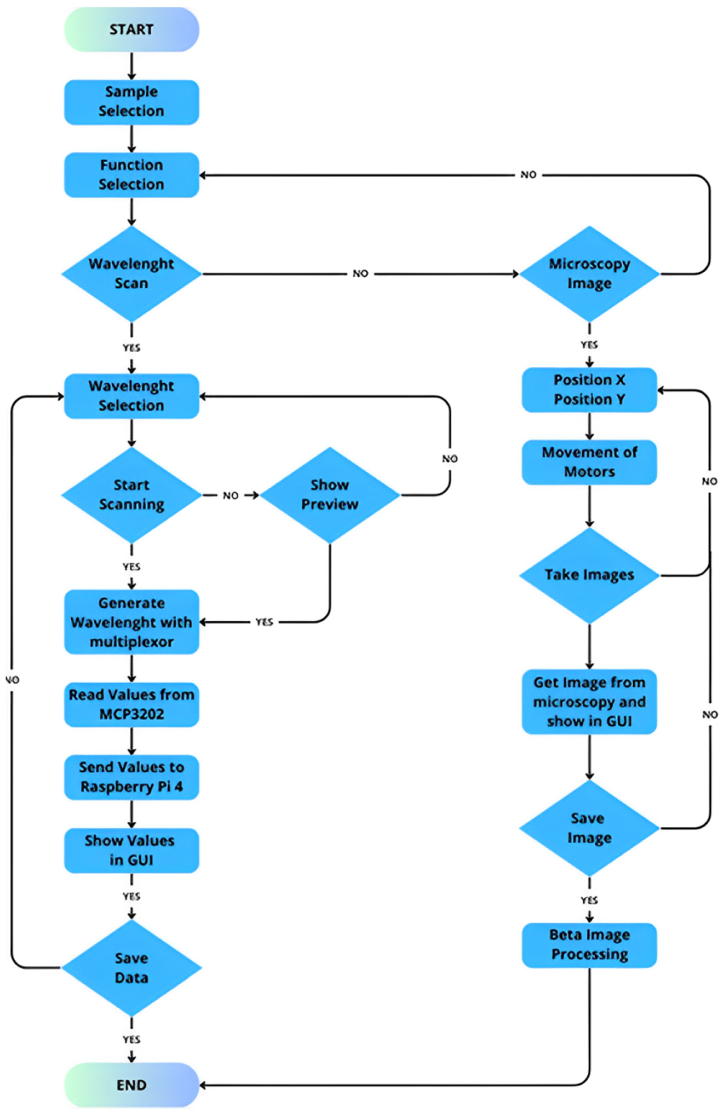
3.1. Operation and Data Acquisition

The operation of the prototype sensor involves a coordinated sequence of steps designed to effectively detect and analyze microplastics. The workflow is as follows:
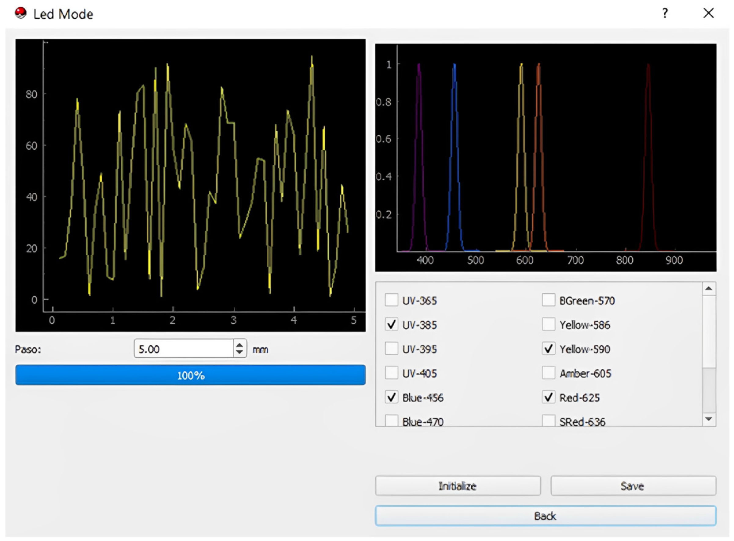
  • The process commences with the selection of wavelengths to scan the sample using the multiplexer, ensuring precise and targeted analysis of the material;
  • Then, the four-bar structure performs a systematic scan across the filter containing microplastics, ensuring comprehensive coverage of the sample area;
  • During the scan, the photodiode captures the transmitted light from the microplastics. The absorbance intensity varies depending on the material’s optical properties;
  • The photodiode generates an analog signal, which we route through an analog-to-digital converter (ADC) circuit that digitizes it for further processing;
  • The Raspberry Pi processes the digitized data, identifying peaks in the signal that correspond to specific wavelengths. These peaks provide critical information about the sample’s optical response;
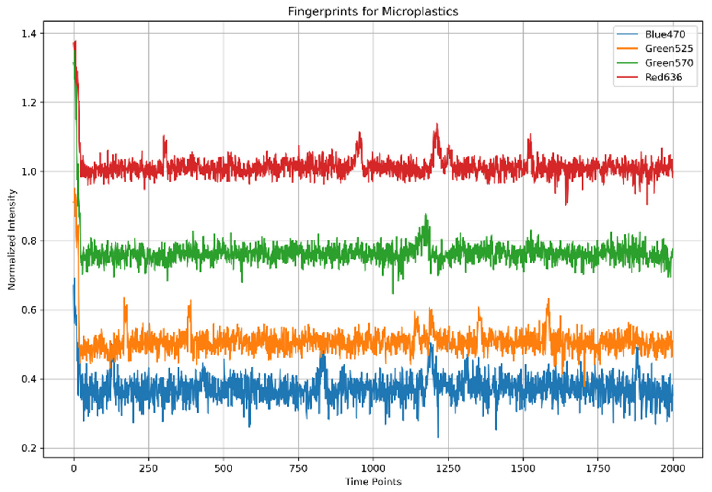
  • Finally, the intensity of the detected signals determines the identification of the microplastics. The system utilizes these intensity patterns to differentiate microplastics from other materials in the sample.
The prototype’s operational workflow allows it to efficiently acquire and process data, enabling the rapid identification of microplastics in diverse sample environments. The integrated mechanism, photodiode, and ADC circuit ensure high-resolution scanning, while Raspberry Pi’s processing capabilities support accurate signal analysis. Together, these components form a robust, portable solution for precisely detecting microplastics.

3.2. Operation in an Uncontrolled Environment

The initial stage entailed the evaluation of the sensor within an uncontrolled environment, thereby simulating real-world conditions characterized by unregulated variables. Figure 13, Figure 14 and Figure 15 show the prototype and the cloth that will be used for testing. This step establishes a baseline for evaluating the sensor’s adaptability and resilience to external factors. This preliminary stage is analogous to a field test, wherein the sensor’s adaptability and resilience to unpredictable factors are assessed.
We assessed the sensor in an open environment with low light, where we observed peak signals of 0.2 V. When the white light of an Asus ROG Phone 6 was directed towards the sensor, the light intensity increased to 2.6 V. Utilizing a handheld flashlight with a 130-lumen output at a distance of 10 cm resulted in the successful saturation of the sensor to 3.3 volts. Over the course of testing with the blue (456 nm) and green (570 nm) wavelengths, the sensor yielded varying results, with 1.1 volts being produced for the blue wavelength and 1.3 volts for the green wavelength. Consequently, the efficacies of the noise reduction filter and the amplification function were confirmed. The motors can be adjusted to select a specific position and scan the sample.

3.3. Operation in a Controlled Environment

The second stage of the experiment transitions into a controlled environment, where we manipulate variables to observe the sensor’s response to specific conditions. We conducted meticulously controlled tests to eliminate extraneous variables that could affect the data, ensuring accurate and reliable measurements. Our method incorporates a nocturnal testing phase to ensure the stability of parameters and to mitigate the impact of extraneous light sources on sensor readings. It should be noted that this approach is not the sole option, and alternative methods may also prove effective. We optimize the conditions by using a black fabric tarp to obstruct external light sources and schedule tests after 11:00 PM, ensuring that the green light beam remains the only variable influencing the sensor readings.
The prototype underwent testing and calibration in a controlled setting using wavelengths in the green and blue spectral ranges. This process generated a spectrum based on the attenuation value obtained by the sensor. It is noteworthy that a dataset comprising 2000 values was collected. Analysis of the prototype’s graph revealed that the sensor’s response plateaued at approximately 500 values, after which it stabilized. This observation persisted, prompting the collection of an extensive dataset to determine if any potential disturbances occurred beyond this point. Additionally, measurements were conducted in the presence of noise to evaluate its impact on the signal, ensuring a comprehensive understanding of the sensor’s behavior.
The high volume of data points collected per measurement can facilitate a detailed statistical analysis, enabling the identification of any anomalies or patterns within the data. With such a dataset, one could employ various analytical techniques, such as regression analysis, standard deviation calculations, and hypothesis testing, to draw meaningful conclusions about the green light’s properties and effects.

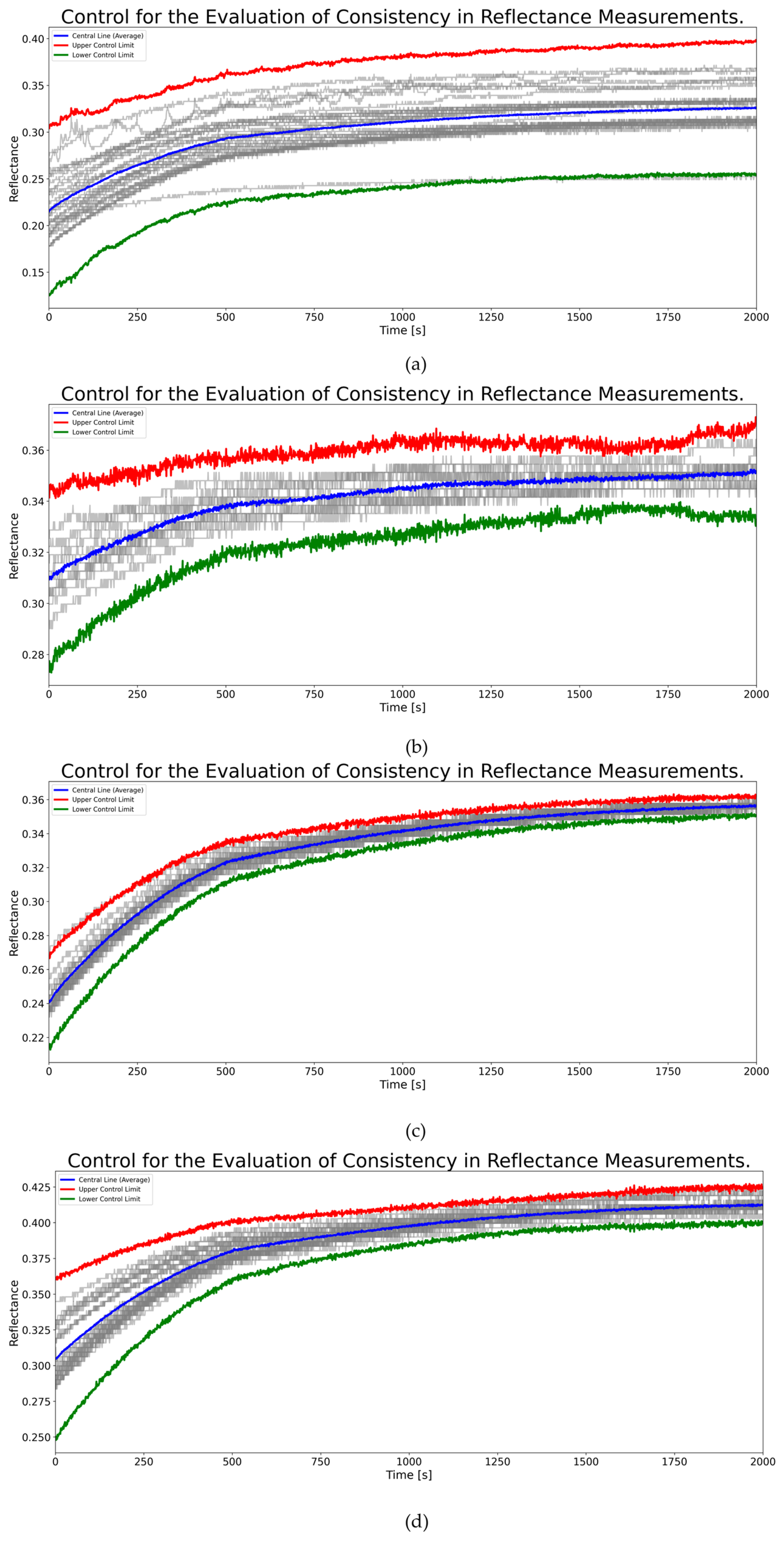
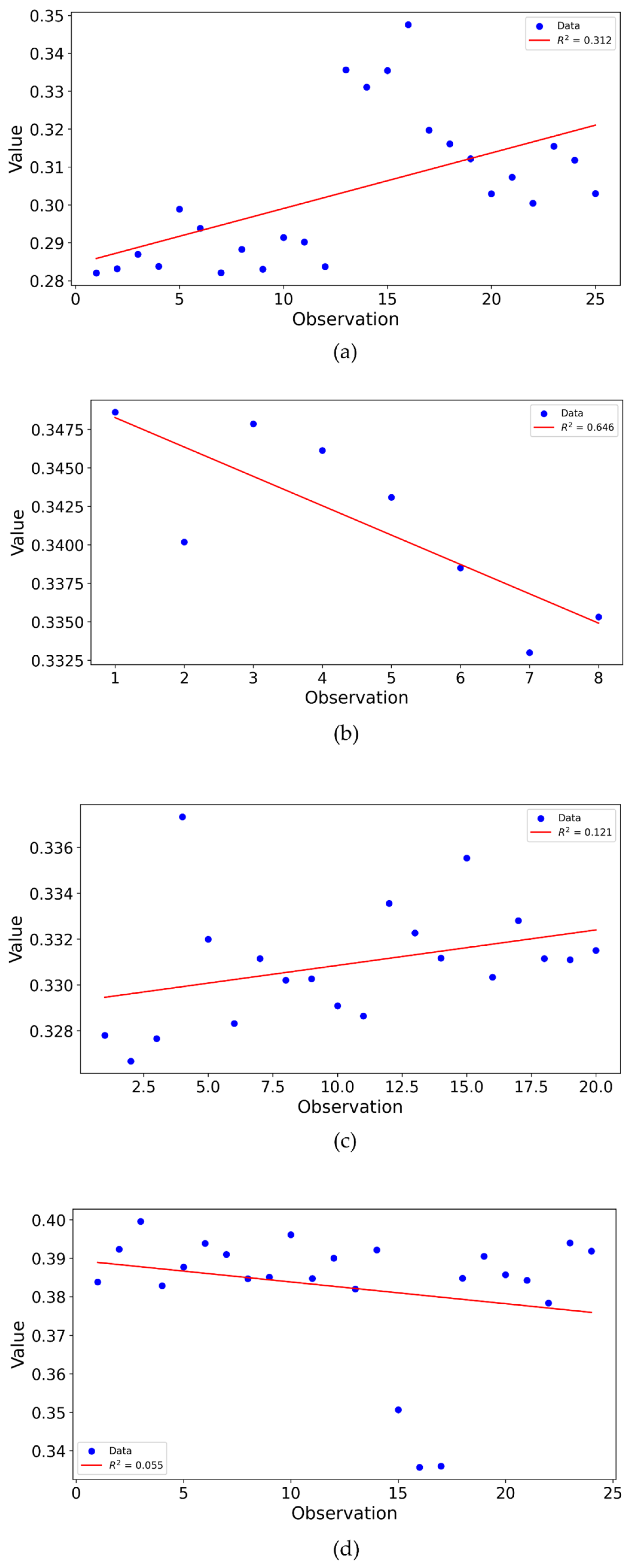
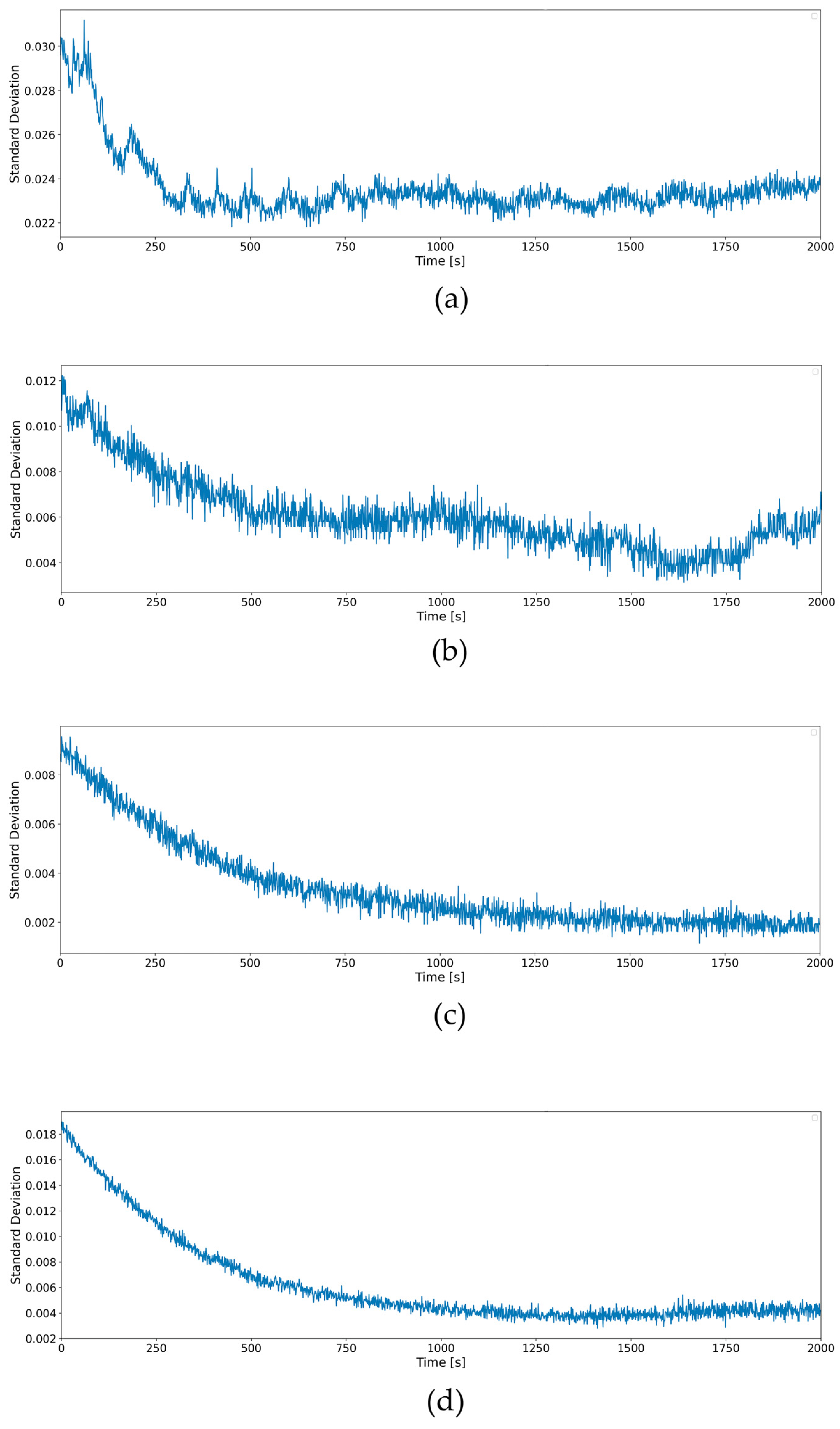
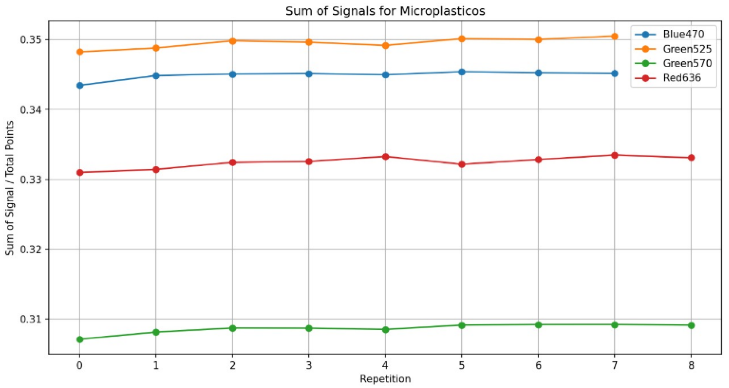
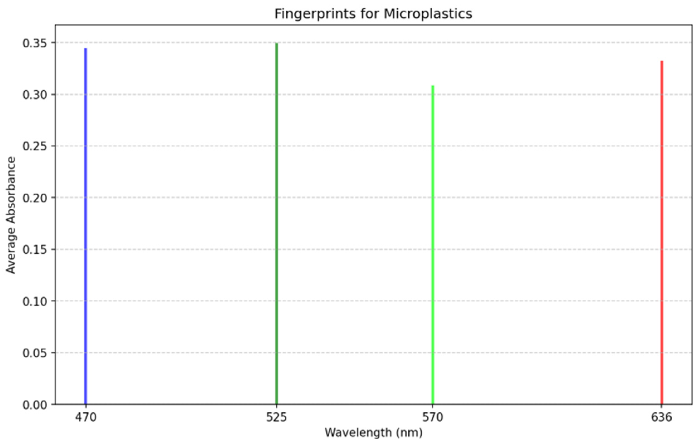
3.4. Reproducibility and Statistical Analysis

The curve analysis is critical to understanding a dataset’s behavior, especially when the relationship involves continuous variables. Repeatability in curve analysis is essential for reliable, reproducible results. Distance from the sample and operator skill level can affect reproducibility, leading to inconsistent results. We rely on standard procedures and training to mitigate these issues.
Optics introduce variability due to differences in light paths and focal lengths. We account for these differences in the analysis. The average and standard deviation provide insights into the central tendency and dispersion of the data. Chebyshev’s theorem estimates the minimum proportion of observations within a certain number of standard deviations from the mean, providing a bound on the data’s variability. Figure 16 shows control charts based on Chebyshev’s theorem, which identifies variability in the reflectance measurements. Using the data, we calculated the upper (red) and lower (green) control limits as three standard deviations above and below the mean (blue line). The points within these limits demonstrate controlled variability in the measurements, indicating stability during testing.
Figure 17 presents the quadratic error analysis for green and blue lasers, with and without optics. The error peaks indicate moments of greater variability, potentially linked to external interferences or optical system adjustments. These findings emphasize the importance of calibrating sensors optimally, particularly in setups without optics.
Functional data analysis (FDA) is another statistical approach that considers data in curves, surfaces, or other continuous variations. FDA is beneficial when the data points are highly correlated, allowing for the analysis of data that vary over a continuum, such as time or wavelength. In the context of the FDA, error handling and variance estimation play crucial roles in interpreting functional data. The reflectance curves analyzed in this study are typical examples of functional data, where each curve represents a continuous function over time. These curves vary not only in their point values but also in their global structures, requiring a statistical approach that can capture these complexities. The variance in FDA describes how the functions (reflectance curves, in this case) are dispersed around the functional mean. In practical terms, variance quantifies the variability of the curves between different measurements or experimental conditions. In studying the reflectance curves of different laser configurations, functional variance helps us understand how much the curves change in response to changes in laser configuration or the introduction of optical components.
Standard methods to analyze this variance include mean function plots and confidence bands that represent functional confidence intervals (Figure 18). These methods visualize where and how the curves deviate significantly from the mean, offering insights into the stability and consistency of the studied laser configurations. We also evaluated temporal dispersion by plotting the time-resolved standard deviation for each configuration (Figure 19), which shows that incorporating optics systematically reduces variability and accelerates convergence toward a stable baseline.
Understanding error and variance in an FDA is key for validating the accuracy of reflectance measurements and optimizing device configurations used in optical experiments. By identifying configurations that minimize variance and error, researchers can improve the reproducibility of their experiments and increase the reliability of their conclusions. Implementing FDA techniques for reflectance curve analysis in this study allows for a robust evaluation of the effects of different laser configurations, ensuring that decisions based on these analyses are well-founded and statistically valid.

3.5. Functional Variance Analysis of Reflectance Measurements with Different Laser Configurations

A Functional analysis of variance (FANOVA) was performed using a linear mixed model to investigate the influence of laser configurations on the reflectance measurements. The dataset consisted of the average reflectance values obtained at regular time intervals for blue and green lasers, both with and without optics. Grouping measurements by time intervals facilitated a direct comparison between the configurations and accounted for the inherent temporal dependence of the functional data.
The linear mixed model was fitted with reflectance as the dependent variable and laser configuration as the independent variable. Fixed terms were included for each configuration, while a random term captured intra-group variations associated with repeated measurements. This approach effectively addressed the correlation within time groups.
Statistical analysis revealed significant differences in reflectance measurements across configurations. For instance, the green laser without optics exhibited a substantial increase in reflectance (+0.028 units, z = 102.427, p < 0.001) compared to the reference configuration, the green laser with optics. Similarly, the blue laser with optics showed a more significant increase ( + 0.047 units, z = 171.488 , p < 0.001 ), while the blue laser without optics presented a reduction in reflectance ( 0.010 units, z = 36.813 , p < 0.001 ). These results underscore the impact of both laser color and the presence of optics on reducing variability and enhancing measurement precision. A summary of the estimated coefficients, confidence intervals, and p-values is provided in Table 2.
Our analysis estimated the group variance to be 0.001, indicating that the measurements remain significantly homogeneous over time within each configuration. However, the model’s convergence limitations suggest caution when interpreting this parameter. These coefficients confirm that subtle adjustments in laser configuration systematically influence reflectance, a finding that is particularly notable for practical applications in both controlled and experimental environments.
Statistical results reinforce the prototype’s robustness in detecting microplastics under various experimental configurations. The integration of FANOVA and control charts enables the identification of optimal setups, such as lasers equipped with optics, which demonstrate reduced variability and improved precision. These findings also emphasize the relevance of carefully selecting optical components based on the specific requirements of the experiment or application.
This methodology highlights the importance of accounting for temporal structure and intra-group correlation when analyzing functional data. Linear mixed models offer a flexible and robust framework for assessing the impact of categorical variables on functional measurements, allowing for precise adjustments for dependencies and variability within groups.
The experimental functionality of the microscope is currently operational, allowing for image acquisition of microplastics and other materials. Although this feature is still in the beta phase, it enables initial image processing for material detection. For specific cases, sample calibration remains a critical step that has yet to be fully implemented. Once samples are detected, the microscope functionality allows for verification of the material’s identity before proceeding with a spectroscopic analysis to confirm its composition.
The sensor has been engineered to optimize sample analysis by facilitating the autonomous processing of numerous samples, thereby reducing reliance on external laboratories and their time-consuming procedures. It facilitates instant detection and precise localization, enabling researchers to visually confirm their findings using a microscope. This innovation addresses the challenges associated with conventional bulk sample analysis, which frequently necessitates substantial time and manual effort. Furthermore, the sensor’s capacity for remote operation enhances its versatility, making it applicable across a wide range of research environments.

3.6. Beta Test of Absorption in Real Life Environment

In the experimental phase, four distinct lasers—red, green, bright green (yellow), and blue—were utilized, as detailed in the experimental section. The samples were irradiated, and absorbance values were obtained using the BPW34 sensor following the previously established calibration procedure. This setup ensured consistency and allowed for a reliable comparison across different laser configurations.
The first sample set consisted of microplastics placed on the right side of a microscope slide, with a thickness not exceeding 0.8 mm (Figure 20).
On the left side of the slide, a 2 × 2 cm section of the outer layer of a golden apple hypanthium was positioned to serve as the organic reference material. The tests were conducted seven times in an uncontrolled environment to evaluate the variability of the measurements and assess the equipment’s portability for use in various locations.
The samples were radiated and then saved in a CVS file and were ready for analysis for each wavelength. This is shown in Figure 21 and Figure 22.
Normalized signals for each laser wavelength (470 nm, 525 nm, 570 nm, and 636 nm) were obtained for both microplastics and organic samples. These signals are shown in Figure 23 for microplastics and in Figure 24 for organic materials. As expected, organic materials consistently exhibited higher light transmittance and lower absorbance compared to microplastics, aligning with theoretical predictions. This behavior is crucial for the rapid and reliable identification of microplastics within mixed samples.
Additionally, as the wavelength shifted toward the red and infrared regions of the spectrum, microplastics exhibited lower absorbance, as illustrated in Figure 25. This trend suggests that microplastics are more easily distinguishable at these wavelengths, providing a practical advantage for detection systems designed to operate within this spectral range.
We calculated the average absorbance for each test to facilitate material classification, yielding unique optical fingerprints for microplastics and organic samples (Figure 26 and Figure 27). These fingerprints provide a foundation for implementing advanced classification methods, such as fuzzy logic or neural networks. The calculated voltage values represent the material’s signature and can be directly employed to train classification models.
The experimental results underscore the potential for integrating intelligent systems into the prototype. Future work aims to develop robust classification algorithms capable of distinguishing materials in real-time by leveraging optical fingerprints. These advancements would significantly enhance the prototype’s versatility and usability, particularly in scenarios requiring rapid, on-site analysis.

3.7. Microscopy and Image Processing

The microscope verifies microplastics in the samples. Depending on the experimental requirements, the sensor can operate in two modes: microscope then light source, or light source then microscope. It is a digital Chiciris model with USB 2.0 connectivity offering 50× to 1000× magnification. Its portability and ability to seamlessly integrate Raspberry Pi 4 make it suitable for field and controlled laboratory applications.
In microscope mode, the sample is first focused, and an image of the area of interest is captured. The image is then processed using a series of algorithms designed to detect microplastics based on their morphological characteristics. The initial step involves applying a grayscale filter to the image. This transformation converts the RGB (red, green, blue) color channels into a single-channel grayscale representation using the following equation:
G r a y = 0.6 R + 0.3 G + 0.1 B
Equation (6) is the grayscale conversion equation.
The grayscale value is calculated by combining the red, green, and blue channels, weighted by coefficients that sum to one. This ensures that the image keeps proper brightness and contrast. However, it should be noted that this method has inherent limitations. The coefficients must be between zero and one, and their sum must equal one.
The next step is binarization, which turns the pixel values into zero or one based on a set threshold. Noise is removed using morphological operations, starting with closing and followed by opening. The cleaned binary image is subtracted from the original to emphasize object borders, which are further improved with Canny edge detection. Skeletonization refines the edges, creating a clearer outline of the detected structures.
After completing the image-processing stage, microplastics are detected. Objects in the processed image are segmented using chain code to outline their boundaries. These segmented objects are then analyzed based on parameters such as color, fractal dimension, centroid distance, width, and height. The topology summary focuses on four main types—fragments, pellets, fibers, and flakes—since they are the most common and easiest to identify [43]. The implemented methods include the following:
  • Gray filter application: we apply a gray filter to the initial images;
  • Gaussian filter application: we use a Gaussian filter to smooth the images;
  • Binarization: we binarize the images to distinguish microplastics from the background;
  • Morphological operations: we perform closing and opening operations to refine shapes and remove noise;
  • Dilation and erosion: before skeletonization, we apply dilation followed by erosion to remove smaller objects from the image;
  • Edge detection: We detect edges by subtracting the binarized image after applying a closing operation. This process is efficient and less computationally expensive, making it suitable for processing on a Raspberry Pi;
  • Skeletonization: We apply skeletonization to all objects in the image to accurately analyze their structure;
  • Chain code application: after skeletonization, we apply chain code to count the number of objects within the image;
  • Morphology determination: we use polynomial approximation and fractal dimension analysis to determine the morphology of each object within the image, which makes it easier to classify them.
These methods help identify and describe the microplastics based on their shape, creating a solid foundation for further research and use in environmental monitoring.

3.8. GUI Usability and Impact on User Experience:

The developed GUI is designed to facilitate user interaction with the prototype, making it more user-friendly. It allows users to select the number of samples to run (one, two, or three) and choose specific LEDs for data collection. This customizable interface enables users to operate the prototype efficiently and tailor the settings to their needs. Our research group has found the prototype more suitable for use with the GUI, as it enhances operational ease and reduces the learning curve for new users.
Although GUI enhances user interaction, it has some limitations. The system only supports partial automation, requiring users to manually choose parameters and LEDs. This study focuses on the LED mode, and detailed image analysis is excluded, as it is covered in a separate short communication on image-processing techniques for identifying microplastics.

3.9. Operation Limits

The research setup has shown the ability to detect microplastics ranging from 0.5 mm to 5 mm, covering the most common sizes found in environmental samples.
  • Surface scanning and sample analysis: The sensor scans the surface, up to 20 cm2 per run, allowing it to analyze a large sample area efficiently. The system can process up to three samples per run, thanks to the three custom-made sample holders and the laser holder’s specific design in a C-shaped form;
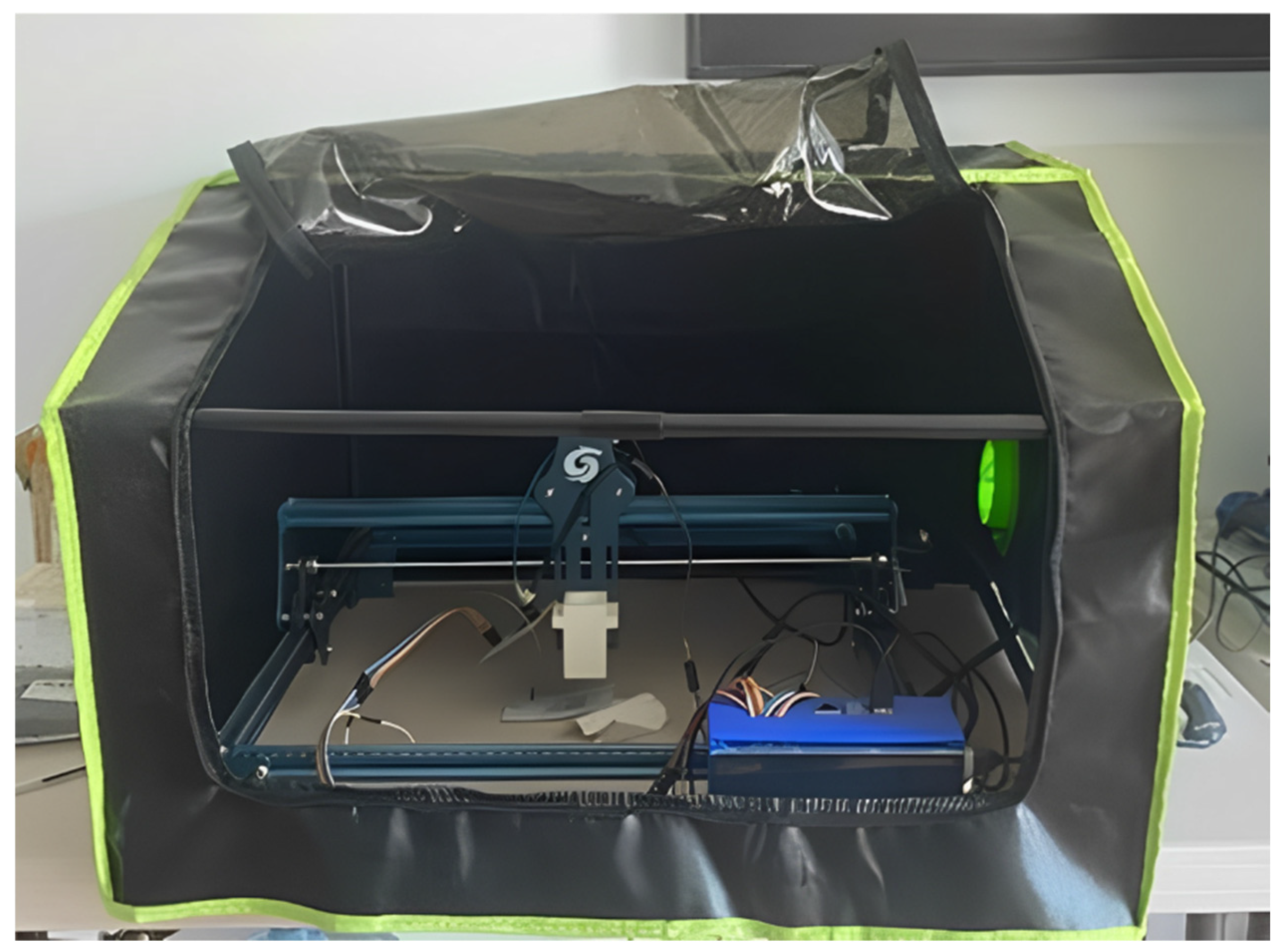
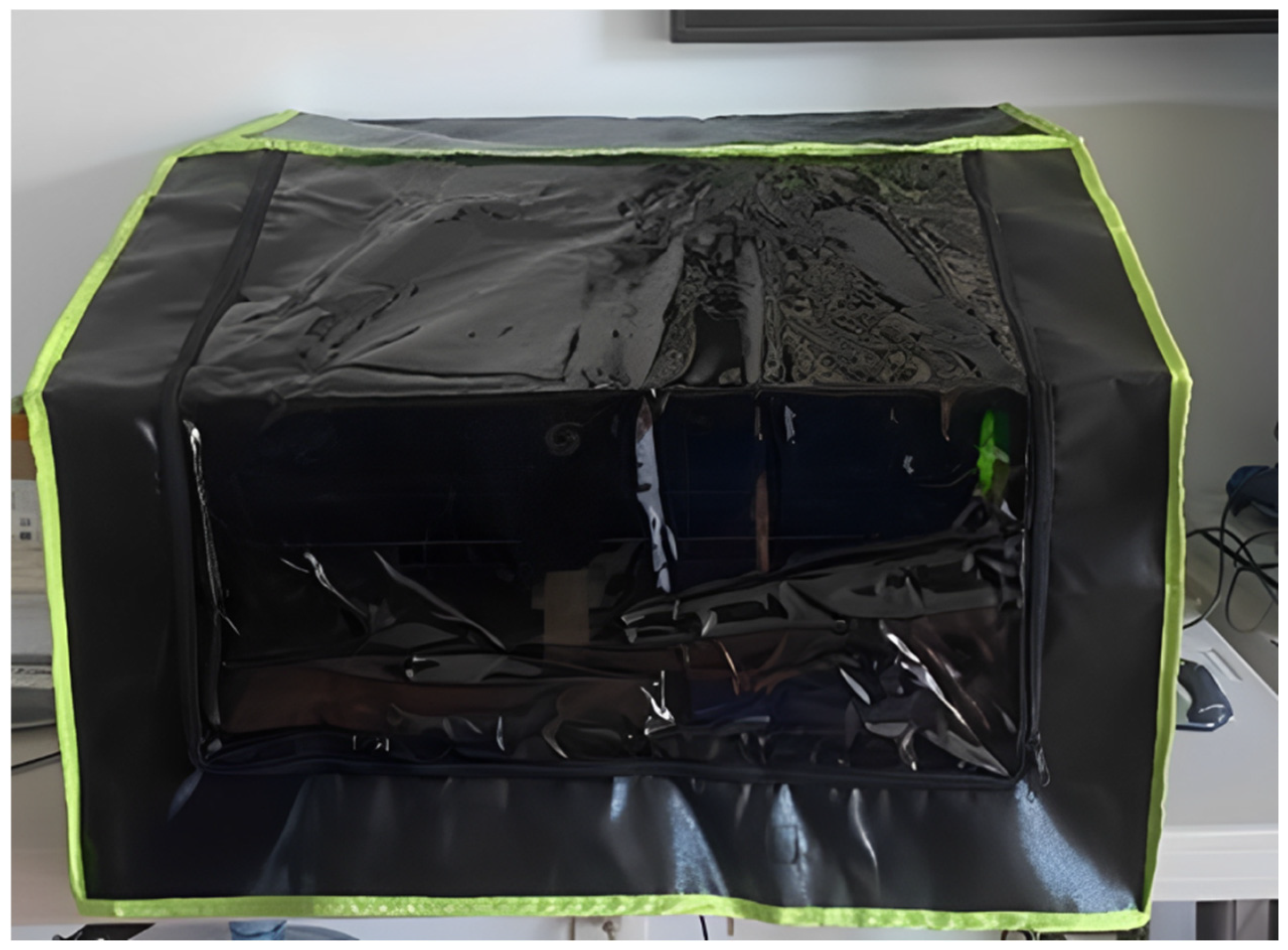
  • Luminosity and environmental conditions: One limitation found during testing is the effect of ambient light. Bright environments can cause detection errors, so a black cloth is needed to reduce light interference during the measurements. The sample should be placed 1.2 to 2 cm away to ensure accurate reading;
  • Specificity: Digital image processing (DIP) techniques improve the sensor’s ability to differentiate microplastics from other particles by analyzing their morphological characteristics. This issue is further explored in another published study [28]. This precision is important for reliable environmental monitoring and avoids mistakes in detecting microplastics.
We evaluated the sensor’s performance by calculating its sensitivity and limit of detection (LOD) as follows:
  • Sensitivity: sensitivity (S) was determined as the slope of the calibration curve, representing the change in signal intensity per unit concentration of microplastics:
S = Δ V Δ C
Equation (7) is the sensitivity equation.
where ΔV is the change in the detected voltage output, and ΔC is the change in microplastic concentration (e.g., grams per liter).
  • Limit of Detection (LOD): the LOD is defined as three times the standard deviation of the blank sample ( σ b ) divided by the slope (S) of the calibration curve:
    L O D = 3 σ b S
Equation (8) is the limit of detection equation.
This equation ensures that the sensor’s detection threshold accounts for natural variability in blank readings, thereby making it reliable for identifying microplastic presence at low concentrations.

3.10. Comparison with Conventional Techniques

We compared the performance of our sensor with that of conventional techniques, including FTIR spectroscopy, Raman spectroscopy, and UV-Vis spectroscopy. The Table 3 below highlights the key features of the standard microplastic detection methods alongside the developed sensor. FTIR and Raman spectroscopy offer high selectivity and precision in molecular identification, but they are expensive, require sample preparation, and are not portable. The developed sensor addresses these limitations, offering rapid analysis, minimal preparation, and field portability, making it an accessible tool for researchers conducting preliminary microplastic analysis.
The prototype achieves sensitivity comparable to that of UV-Vis spectroscopy, effectively identifying the presence of microplastics in controlled conditions. Unlike FTIR and Raman spectroscopy, which detect particles as small as 1 µm and provide detailed morpho-chemical analysis (as highlighted in Xu et al. and Prata et al.), the prototype is designed for practical use and accessibility in different environments. It quickly detects potential microplastic contamination, allowing researchers to identify polluted samples without needing specialized laboratory equipment.
This device combines functionality and simplicity. It combines optical sensing with mechanical and electronic precision to provide reliable results without the high cost or complexity of traditional methods. Moreover, its rapid detection capabilities help researchers process samples quickly and avoid unnecessary analysis. These strengths make the prototype a practical tool for addressing microplastic pollution in research and field work.

4. Conclusions

In conclusion, the development of the sensor prototype presented in this study offers an innovative solution to the pressing issue of microplastic pollution. The integration of mechanical precision, electronic control, and optical sensing enables the effective detection of microplastics, achieving a balance between functionality and accessibility. The following conclusions summarize the main findings, implications, and future opportunities emerging from this work:
  • Integrated approach: This study presents a novel sensor prototype that combines precise mechanical design, electronic control, and optical sensing to effectively detect microplastics. The necessity of integrating diverse technological approaches to confront this pressing environmental concern is underscored by the interdisciplinary nature of the study;
  • Controlled testing and future applications: To ensure accuracy and reproducibility, the prototype was developed and tested in a controlled environment using commercial PLA microplastics. In addition, future applications may include the deployment of the prototype in real-world environments, such as rivers, oceans, or mountains, for on-site detection. This approach should eliminate the need for subsequent visits to collect additional samples if no microplastics are found. As a result, it would help conserve resources and save time;
  • Advanced detection mechanism: The detection is conducted by directing a light source through the samples and measuring the intensity in volts. This method is a reliable way to identify microplastics through absorbance (“experimental absorbance” or “attenuance”) tests.
  • Validation and sensitivity: We measured the prototype’s sensitivity and detection limits with absorbance and attenuation equations. We tested the system with commercial PLA microplastics to ensure accuracy. The prototype cannot measure particles as small as FTIR or Raman, but it identifies microplastics in the visible and near-infrared spectrum through light attenuation. It has been validated by comparison with other methods and can process multiple samples efficiently, making it a useful tool for environmental analysis;
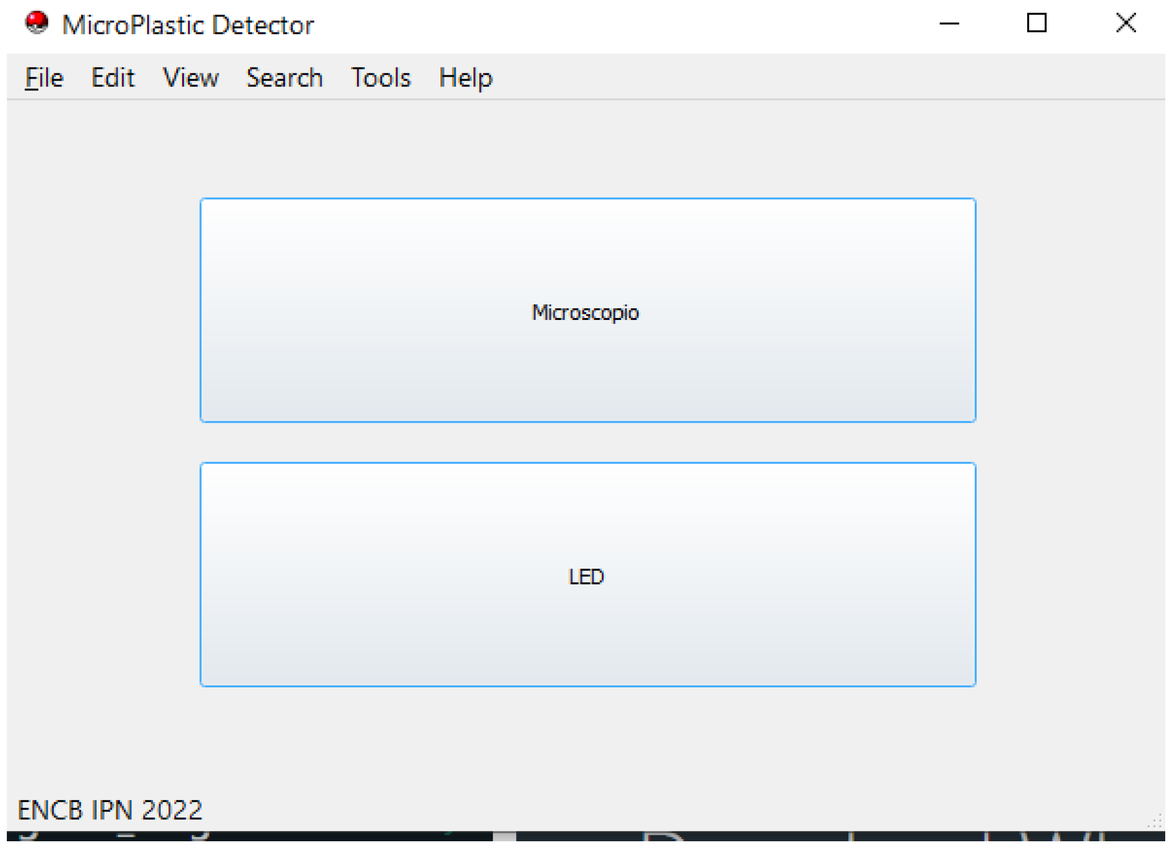
  • Technological innovation: The system uses LEDs with specific wavelengths and a Raspberry Pi 4 to control them. It also includes stepper motors for precise movement, making the setup efficient and accurate. The incorporation of filters serves to eliminate external noise and ensure the accuracy of the measurements. A graphical user interface (GUI) facilitates operations through two modes: microscopy and LED-based detection;
  • Portable and versatile design: The prototype’s modular and portable design allows it to be used in both laboratory and field applications. This flexible approach overcomes the current limitations of traditional detection methods, such as FTIR and Raman spectroscopy, which are often expensive and less flexible.

Future Research and Expansion

In future research, the prototype could be improved in a number of different directions. One possibility is to adapt it for use in environments such as rivers, oceans, and mountains, which would allow direct testing of samples and reduce the need for additional visits if no contamination is found. Another potential direction is to integrate machine-learning algorithms and Adalin networks to enhance classification and detection accuracy. Additionally, creating a database of material fingerprints could help identify microplastics in a larger range of polymers.

Author Contributions

The contributions of each author to this article can be summarized as follows: M.C.-L. was the primary author and contributed to the methodology, software, investigation, and writing. R.A.-G. provided writing corrections and curated the data. D.E.G.-R., V.I.M.-L. and M.M.G.-L. contributed significantly to editing, with M.M.G.-L. also contributing ideas. M.A.R.-G. engaged in methodology, data analysis, writing, editing, and supervision. Á.G.-S. participated in writing, editing, and methodology. V.G.-F. was responsible for supervising, editing, and visualization. Lastly, J.A.M.-P. oversaw supervision, conceptualization, and project management. Each author’s initials are used to respect their privacy and acknowledge their intellectual contributions. All authors have read and agreed to the published version of the manuscript.

Funding

This research was made possible by the generous support of the Secretaría de Ciencia, Humanidades, Tecnología e Innovación (SECIHTI), before named Consejo Nacional de Humanidades, Ciencias y Tecnologías (CONAHCyT) and the Instituto Politécnico Nacional-Escuela Nacional de Ciencias Biológicas (IPN-ENCB), Research and Graduate Secretary (SIP) project (20220263, 20230338, and 20241771). The doctoral scholarship grants, no. 715605 and 1076666, held by Ricardo Aguilar-Garay and Maximiliano Campos-López. Ricardo Aguilar-Garay and Maximiliano Campos-López are students in the Programa de Doctorado en Nanociencias y Micro-Nanotecnologías at the Escuela Nacional de Ciencias Biológicas, Instituto Politécnico Nacional.

Institutional Review Board Statement

Not applicable.

Informed Consent Statement

Not applicable.

Data Availability Statement

The raw data supporting the conclusions of this article will be made available by the authors on request.

Acknowledgments

I would like to express my deepest gratitude to the Instituto Politécnico Nacional and CONACYT for their unwavering support and invaluable resources. Special thanks are also given to UPIITA for providing the necessary facilities and environment conducive to research. Lastly, I am immensely thankful to my advisors, whose guidance and insights have been instrumental in completing my work. Their dedication and expertise have significantly shaped this project and contributed to my professional growth.

Conflicts of Interest

The authors declare no conflicts of interest.

Abbreviations

The following abbreviations are used in this manuscript:
MPsMicroplastics
RMSRaman Spectroscopy
FTIRFourier-Transform Infrared
ABSAcrylonitrile Butadiene Styrene
PLAPolylactic Acid
PETPolyethylene Terephthalate
CNCComputer Numerical Control
LEDLight-Emitting Diode
GUIGraphical User Interface
UIUser Interface
LEDLight Emitting Diode
PCBPrinted Circuit Board
DIPDigital Image Processing
NEMANational Electrical Manufacturers Association
GPIOGeneral-Purpose Input/Output
ADCAnalog-to-Digital Converter
OP-AMPOperational Amplifier
DEMUXDemultiplexer
UVUltraviolet
FDAFunctional Data Analysis
FANOVAFunctional Analysis of Variance

References

  1. Frias, J.P.G.L.; Nash, R. Microplastics: Finding a consensus on the definition. Mar. Pollut. Bull. 2019, 138, 145–147. [Google Scholar] [CrossRef] [PubMed]
  2. Atkinson, J.T.; Su, L.; Zhang, X.; Bennett, G.N.; Silberg, J.J.; Ajo-Franklin, C.M. Real-time bioelectronic sensing of environmental contaminants. Nature 2022, 611, 548–553. [Google Scholar] [CrossRef] [PubMed]
  3. Ghosh, S.; Sinha, J.K.; Ghosh, S.; Vashisth, K.; Han, S.; Bhaskar, R. Microplastics as an Emerging Threat to the Global Environment and Human Health. Sustainability 2023, 15, 10821. [Google Scholar] [CrossRef]
  4. Lehner, R.; Weder, C.; Petri-Fink, A.; Rothen-Rutishauser, B. Emergence of Nanoplastic in the Environment and Possible Impact on Human Health. Environ. Sci. Technol. 2019, 53, 1748–1765. [Google Scholar] [CrossRef]
  5. Pham, D.T.; Kim, J.; Lee, S.-H.; Kim, J.; Kim, D.; Hong, S.; Jung, J.; Kwon, J.-H. Analysis of microplastics in various foods and assessment of aggregate human exposure via food consumption in korea. Environ. Pollut. 2023, 322, 121153. [Google Scholar] [CrossRef]
  6. Synani, K.; Abeliotis, K.; Velonia, K.; Maragkaki, A.; Manios, T.; Lasaridi, K. Environmental Impact and Sustainability of Bioplastic Production from Food Waste. Sustainability 2024, 16, 5529. [Google Scholar] [CrossRef]
  7. Nampoothiri, K.M.; Nair, N.R.; John, R.P. An overview of the recent developments in polylactide (PLA) research. Bioresour. Technol. 2010, 101, 8493–8501. [Google Scholar] [CrossRef]
  8. Liu, F.-F.; Wang, S.-C.; Zhu, Z.-L.; Liu, G.-Z. Current Progress on Marine Microplastics Pollution Research: A Review on Pollution Occurrence, Detection, and Environmental Effects. Water 2021, 13, 1713. [Google Scholar] [CrossRef]
  9. Baruah, A.; Sharma, A.; Sharma, S.; Nagraik, R. An insight into different microplastic detection methods. Int. J. Environ. Sci. Technol. 2022, 19, 5721–5730. [Google Scholar] [CrossRef]
  10. Joshi, A.; Akhtar, N.; Kumar, A. Microplastics Detection Techniques BT-Microplastics Pollution and its Remediation; Kumar, A., Singh, V., Eds.; Springer Nature: Singapore, 2024; pp. 25–53. [Google Scholar] [CrossRef]
  11. Chen, Q.; Wang, J.; Yao, F.; Zhang, W.; Qi, X.; Gao, X.; Liu, Y.; Wang, J.; Zou, M.; Liang, P. A review of recent progress in the application of Raman spectroscopy and SERS detection of microplastics and derivatives. Microchim. Acta 2023, 190, 465. [Google Scholar] [CrossRef]
  12. Thomas, D.; Schütze, B.; Heinze, W.M.; Steinmetz, Z. Sample Preparation Techniques for the Analysis of Microplastics in Soil—A Review. Sustainability 2020, 12, 9074. [Google Scholar] [CrossRef]
  13. Subharthe, S.; Clarke, B. From Collection to Analysis: A Practical Guide to Sample Preparation and Processing of Microplastics. Agilent, 2024. Available online: https://www.agilent.com/cs/library/technicaloverviews/public/te-microplastics-sample-preparation-guide-8700-ldir-5994-7587en-agilent.pdf (accessed on 25 February 2025).
  14. Vojnović, B.; Mihovilović, P.; Dimitrov, N. Approaches for Sampling and Sample Preparation for Microplastic Analysis in Laundry Effluents. Sustainability 2024, 16, 3401. [Google Scholar] [CrossRef]
  15. Xu, G.; Cheng, H.; Jones, R.; Feng, Y.; Gong, K.; Li, K.; Fang, X.; Tahir, M.A.; Valev, V.K.; Zhang, L. Surface-Enhanced Raman Spectroscopy Facilitates the Detection of Microplastics <1 μm in the Environment. Environ. Sci. Technol. 2020, 54, 15594–15603. [Google Scholar] [CrossRef]
  16. Prata, J.C.; da Costa, J.P.; Lopes, I.; Duarte, A.C.; Rocha-Santos, T. Environmental exposure to microplastics: An overview on possible human health effects. Sci. Total Environ. 2020, 702, 134455. [Google Scholar] [CrossRef]
  17. Cobos, A.G.Z.; Amón, J.; León, E.; Caballero, P. Standardization of FTIR-Based Methodologies for Microplastics Detection in Drinking Water: A Meta-Analysis Indeed and Practical Approach. Water 2024, 16, 3170. [Google Scholar] [CrossRef]
  18. Willans, M.; Szczecinski, E.; Roocke, C.; Williams, S.; Timalsina, S.; Vongsvivut, J.; McIlwain, J.; Naderi, G.; Linge, K.L.; Hackett, M.J. Development of a rapid detection protocol for microplastics using reflectance-FTIR spectroscopic imaging and multivariate classification. Environ. Sci. Adv. 2023, 2, 663–674. [Google Scholar] [CrossRef]
  19. Nene, A.; Sadeghzade, S.; Viaroli, S.; Yang, W.; Uchenna, U.P.; Kandwal, A.; Liu, X.; Somani, P.; Galluzzi, M. Recent advances and future technologies in nano-microplastics detection. Environ. Sci. Eur. 2025, 37, 7. [Google Scholar] [CrossRef]
  20. Carrieri, V.; Varela, Z.; Aboal, J.R.; De Nicola, F.; Fernández, J.A. Suitability of aquatic mosses for biomonitoring micro/meso plastics in freshwater ecosystems. Environ. Sci. Eur. 2022, 34, 72. [Google Scholar] [CrossRef]
  21. Marcuello, C. Present and future opportunities in the use of atomic force microscopy to address the physico-chemical properties of aquatic ecosystems at the nanoscale level. Int. Aquat. Res. 2022, 14, 231–240. [Google Scholar] [CrossRef]
  22. Oßmann, B.E.; Sarau, G.; Schmitt, S.W.; Holtmannspötter, H.; Christiansen, S.H.; Dicke, W. Development of an optimal filter substrate for the identification of small microplastic particles in food by micro-Raman spectroscopy. Anal. Bioanal. Chem. 2017, 409, 4099–4109. [Google Scholar] [CrossRef]
  23. Taib, N.-A.A.B.; Rahman, R.; Huda, D.; Kuok, K.K.; Hamdan, S.; Bin Bakri, M.K.; Bin Julaihi, M.R.M.; Khan, A. A review on poly lactic acid (PLA) as a biodegradable polymer. Polym. Bull. 2023, 80, 1179–1213. [Google Scholar] [CrossRef]
  24. Mohammadizadeh, M.; Pourabbas, B.; Mahmoodian, M.; Foroutani, K.; Fallahian, M. Facile and rapid production of conductive flexible films by deposition of polythiophene nanoparticles on transparent poly(ethyleneterephthalate): Electrical and morphological properties. Mater. Sci. Semicond. Process. 2014, 20, 74–83. [Google Scholar] [CrossRef]
  25. López Galindo, E.; Sarabia, C.H.; Pérez Aguilar, J.A.; Gómez Vieyra, A. Espectrofotometría del PET y PVC basado en Transmitancia. Rev. Tend. Docencia Investig. Química 2016, 2. Available online: https://zaloamati.azc.uam.mx/items/d5d3556b-64fb-4231-914e-b1f5de1cf6cc (accessed on 18 February 2024).
  26. Martinez-Hernandez, U.; West, G.; Assaf, T. Low-Cost Recognition of Plastic Waste Using Deep Learning and a Multi-Spectral Near-Infrared Sensor. Sensors 2024, 24, 2821. [Google Scholar] [CrossRef]
  27. Endo, T.; Gemma, A.; Mitsuyoshi, R.; Kodama, H.; Asaka, D.; Kono, M.; Mochizuki, T.; Kojima, H.; Iwamoto, T.; Saito, S. Discussion on effect of material on UV reflection and its disinfection with focus on Japanese Stucco for interior wall. Sci. Rep. 2021, 11, 21840. [Google Scholar] [CrossRef]
  28. Campos-Lopez, M.; Aguilar-Garay, R.; Bonilla-Martínez, I.B.; O Gomez-Castrejon, J.; A Mendoza-Pérez, J.; A Reyes-Guzmán, M.; Garibay-Febles, V. Advancing Microplastic Detection Technology through Digital Image Processing, Fractal Analysis, and Polynomial Approximation Methods. Microsc. Microanal. 2024, 30 (Suppl. 1), ozae044.195. [Google Scholar] [CrossRef]
  29. Löder, M.G.J.; Gerdts, G. Methodology Used for the Detection and Identification of Microplastics—A Critical Appraisal BT-Marine Anthropogenic Litter; Bergmann, M., Gutow, L., Klages, M., Eds.; Springer International Publishing: Cham, Switzerland, 2015; pp. 201–227. [Google Scholar] [CrossRef]
  30. Woo, H.; Seo, K.; Choi, Y.; Kim, J.; Tanaka, M.; Lee, K.; Choi, J. Methods of Analyzing Microsized Plastics in the Environment. Appl. Sci. 2021, 11, 10640. [Google Scholar] [CrossRef]
  31. Würth Elektronik eiSos GmbH & Co. KG. Würth Elektronik. 2024. Available online: https://www.we-online.com/de (accessed on 13 December 2023).
  32. Asamoah, B.O.; Kanyathare, B.; Roussey, M.; Peiponen, K.-E. A prototype of a portable optical sensor for the detection of transparent and translucent microplastics in freshwater. Chemosphere 2019, 231, 161–167. [Google Scholar] [CrossRef]
  33. Systemes, D. SolidWorks. SolidWorks Corporation. Available online: https://my.solidworks.com/try-solidworks?mktid=13827&utm_campaign=202007_nam_sw_BINGSWOPT_en_XOP2064_rise_brand_mx_exact&utm_medium=cpc&utm_source=bing&utm_content=search&utm_term=4de94bc1938718e0f04e2de9168f55c0&gclid=4de94bc1938718e0f04e2de9168f55c0&gcl (accessed on 20 January 2024).
  34. Raspberry Pi Foundation. About Us. Available online: https://www.raspberrypi.com/about/ (accessed on 20 January 2024).
  35. Autodesk, Inc. Autodesk EAGLE. Available online: http://eagle.autodesk.com/ (accessed on 20 January 2024).
  36. JLCPCB. Available online: https://jlcpcb.com/ (accessed on 25 January 2024).
  37. Pini, A. The Basics of Photodiodes and Phototransistors and How to Apply Them. Contributed By DigiKey’s North American Editors. Available online: https://www.digikey.com/en/articles/the-basics-of-photodiodes-and-phototransistors-and-how-to-apply-them (accessed on 20 November 2023).
  38. VISHAY. BPW34. Vishay Semiconductors. Available online: https://www.vishay.com/docs/81521/bpw34.pdf (accessed on 15 December 2023).
  39. Slávik, R.; Čekon, M. Correction Factor Estimating of Silicon PIN Photodiode Derived from Outdoor Long-Term Measurement. In Proceedings of the ATF2016 4th Conference on Building Physics and Applied Technology in Architecture and Building Structures, Leuven, Belgium, 15–17 September 2016; Available online: https://www.researchgate.net/publication/311970903_CORRECTION_FACTOR_ESTIMATING_OF_SILICON_PIN_PHOTODIODE_DERIVED_FROM_OUTDOOR_LONGTERM_MEASUREMENT (accessed on 15 December 2023).
  40. Aponte Suárez, R.A.; Serrato Sosa, J.M.; Rojas Castellanos, M.R. Informe №6: Amplificadores Operacionales. April 2015. Available online: https://www.researchgate.net/publication/327656561_Informe_No6_amplificadores_operacionales (accessed on 16 March 2024).
  41. Wohlmuth, C.; Correia, N. User Interface for Interactive Scientific Publications: A Design Case Study BT-Digital Libraries for Open Knowledge; Doucet, A., Isaac, A., Golub, K., Aalberg, T., Jatowt, A., Eds.; Springer International Publishing: Cham, Switzerland, 2019; pp. 215–223. [Google Scholar]
  42. Gram, C. A software engineering view of user interface design BT-Engineering for Human-Computer Interaction. In Proceedings of the IFIP TC2/WG2.7 Working Conference on Engineering for Human-Computer Interaction, Yellowstone Park, WY, USA, August 1995; Bass, L.J., Unger, C., Eds.; Springer: Boston, MA, USA, 1996; pp. 293–306. [Google Scholar] [CrossRef]
  43. Massarelli, C.; Campanale, C.; Uricchio, V. A Handy Open-Source Application Based on Computer Vision and Machine Learning Algorithms to Count and Classify Microplastics. Water 2021, 13, 2104. [Google Scholar] [CrossRef]
Figure 1. The figure shows the spectrum of the blue wavelength at 456 nm, illustrating the peak intensity and bandwidth of the selected LED.
Applsci 15 04757 g001
Figure 2. The figure illustrates a 4-bar linkage system with bidirectional movement along the X and Y axes, resembling a CNC machine setup. The two stepper motors enable precise positioning and maneuvering for detailed surface mapping.
Applsci 15 04757 g002
Figure 3. The figure shows the wiring diagram detailing the connections between the Raspberry Pi, the A4988 stepper motor driver, and the stepper motor. This schematic illustrates how the system enables stepper motor control through GPIO pins.
Applsci 15 04757 g003
Figure 4. The figure shows a flowchart of programming logic implemented on the Raspberry Pi 4. The chart outlines the sequence of operations, including wavelength selection, motor control, data acquisition, and image processing.
Applsci 15 04757 g004
Figure 5. The figure shows the double-sided PCB design. Panel (A) illustrates the physical connections between components, such as LEDs and resistors, while panel (B) presents a detailed electrical schematic.
Applsci 15 04757 g005
Figure 6. The figure shows the spectral sensitivity of the BP34W photodiode, highlighting its detection range from 430 to 1100 nm. The photodiode’s peak sensitivity is at 900 nm, ensuring effective performance across the spectrum [38].
Applsci 15 04757 g006
Figure 7. The figure shows the schematic of the amplifier circuit designed to boost the BPW34 photodiode’s signal. The circuit uses a TLC27L2BCD operational amplifier to achieve high gain and maintain signal integrity [39].
Applsci 15 04757 g007
Figure 8. The figure shows, in section (A), the schematic of a low-pass filter and an analog-to-digital converter circuit implemented with an MCP3202MS and the TLC27L2BCD operational amplifier for noise reduction and improved signal clarity. Section (B) shows the PCB mounted.
Applsci 15 04757 g008
Figure 9. The figure shows the graphical user interface (GUI) layout on the Raspberry Pi screen. The interface supports user interaction for wavelength multiplexing, motor control, and the display of test results in real-time.
Applsci 15 04757 g009
Figure 10. The figure shows the schematic of the light-source mechanism, detailing how the LEDs generate specific wavelengths for interaction with samples.
Applsci 15 04757 g010
Figure 11. The figure illustrates the LED mode interface, showing the operational controls for microplastic detection. The interface features wavelength selection checkboxes, a power slider for adjusting LED intensity, and motor-positioning inputs (“Motor X” and “Motor Y”) for sample alignment. Additional options include initializing the system (“Initialize”), saving configurations (“Save”), and returning to the previous menu (“Back”).
Applsci 15 04757 g011
Figure 12. The figure shows the microscope mode interface, which showcases control options for precise X- and Y-axis motor positioning via dropdown menus. Features include buttons for capturing and saving images (“Snap”! and “Save Snap”!), alongside initialization and configuration options (“Initialize” and “Set Microscope”).
Applsci 15 04757 g012
Figure 13. The figure shows the mounted prototype within a four-bar frame structure designed to support precise movements along the X and Y axes.
Applsci 15 04757 g013
Figure 14. The figure shows the prototype enclosed in a fabric cover designed to eliminate external interferences, such as ambient light and dust. The fabric ensures optimal operating conditions by minimizing noise and preserving the accuracy and reliability of the optical sensing system during microplastic detection.
Applsci 15 04757 g014
Figure 15. The figure shows a fully enclosed prototype featuring a transparent section that allows the user to observe the internal components during operation.
Applsci 15 04757 g015
Figure 16. The figure compares reflectance over time for green (a) without optics and (b) with optics and blue (c) without optics and (d) with optics. Charts display mean reflectance and their upper and lower control limits at ±3 standard deviations. Grey points within these limits illustrate controlled variability, emphasizing improved measurement stability.
Applsci 15 04757 g016
Figure 17. The figure shows the quadratic error comparison over time for reflectance measurements using (a) a green laser without optics, (b) a green laser with optics, (c) a blue laser without optics, and (d) a blue laser with optics. Plots illustrate fluctuations in measurement precision, where peaks indicate increased variability. The progressive error reduction demonstrates the system’s capacity to stabilize, highlighting the beneficial effect of optical components on measurement consistency.
Applsci 15 04757 g017
Figure 18. The figure shows the scatter plots of mean reflectance values for (a) the green laser without optics, (b) the green laser with optics, (c) the blue laser without optics, and (d) the blue laser with optics. Red trend lines with corresponding R2 values indicate the variance explained by linear regression. Lower R2 values indicate stable reflectance across observations, while higher values reflect greater variability, aiding in the assessment of measurement consistency for microplastic detection.
Applsci 15 04757 g018
Figure 19. The figure shows the reflectance variability (standard deviation) over time for four laser configurations: (a) green laser without optics shows high initial variance that stabilizes gradually; (b) green laser with optics exhibits lower overall variance, indicating enhanced precision from optical components; (c) blue laser without optics mirrors the trend in (a), displaying decreasing variance over time; and (d) blue laser with optics has the lowest initial variance, which further decreases, emphasizing optics’ role in improving measurement consistency. These trends underscore the precision and reliability of laser-based microplastic detection.
Applsci 15 04757 g019
Figure 20. The figure shows the experimental setup displaying the placement of microplastics (right) and organic material (golden apple hypanthium, left) on a microscope slide. This arrangement highlights the comparison between synthetic and organic samples for analytical purposes.
Applsci 15 04757 g020
Figure 21. The figure shows the graphical user interface for controlling and monitoring a system in ‘LED Mode’, featuring a graph that displays the voltage value of the wavelength 636 applied to microplastics.
Applsci 15 04757 g021
Figure 22. The figure shows the sensor applying different wavelengths to detect microplastics over deposited microplastics, currently using the 636 nm wavelength.
Applsci 15 04757 g022
Figure 23. The figure shows the normalized intensity profiles for microplastics at four laser wavelengths: blue (470 nm), green (525 nm), bright green (570 nm), and red (636 nm). The figure highlights the stability and distinct signatures of the microplastics across the wavelengths.
Applsci 15 04757 g023
Figure 24. The figure shows the normalized intensity profiles for organic materials at four laser wavelengths: blue (470 nm), green (525 nm), bright green (570 nm), and red (636 nm). Organic samples exhibit higher transmittance and distinct spectral behavior compared to microplastics.
Applsci 15 04757 g024
Figure 25. The figure shows the sum of normalized signals across 7–8 repetitions for microplastics, highlighting the reproducibility of measurements for each laser wavelength.
Applsci 15 04757 g025
Figure 26. The figure shows the average absorbance values for microplastics at laser wavelengths of blue (470 nm), green (525 nm), bright green (570 nm), and red (636 nm). The figure shows lower absorbance in the red and infrared regions, which aids in identification.
Applsci 15 04757 g026
Figure 27. The figure shows the average absorbance values for organic materials at laser wavelengths of blue (470 nm), green (525 nm), bright green (570 nm), and red (636 nm). Organic materials demonstrate a distinct spectral fingerprint compared to microplastics.
Applsci 15 04757 g027
Table 1. A4988 control library reference.
ArgumentNameTypeDescription
1DirectionIntConnects the general-purpose input/output (GPIO) pin that sets the direction of rotation.
2Step_PinIntStep-pin Int connects to the GPIO pin that sets the number of steps.
3Mode_PinsTuple 3 IntMode-pin tuple connects the GPIO that determines the micro-stepping mode.
4Motor_typeStringMotor-type string controller type, for this project, the. A4988” will be used.
Table 2. Estimated coefficients, 95% confidence intervals, and p-values from the functional analysis of variance (FANOVA) for different laser configurations. The table highlights the impact of laser type and the inclusion of optics on reflectance measurements.
ConfigurationEstimated CoefficientConfidence Interval (95%)p-Value
Green laser without optics+0.028[0.026, 0.030]<0.001
Blue laser with optics+0.047[0.045, 0.049]<0.001
Blue laser without optics−0.010[−0.012, −0.008]<0.001
Table 3. Comparison of the developed sensor with conventional techniques, including FTIR, Raman, and UV-Vis spectroscopy.
FeatureFTIR SpectroscopyRaman SpectroscopyUv-Vis SpectroscopyDeveloped Sensor
Detection MechanismAbsorption of infrared lightInelastic scattering of photonsAbsorption of ultraviolet and visible lightAbsorption of multiple wavelengths using LEDs and detection through DIP
Sensitivity RateDetects down to ~20 µm; highly detailed molecular infoDetects as small as 1 µm; exceptional morpho-chemical analysisDetects changes in light absorption for MPs > 100 µmDetects changes in light absorption optimized for MPs > 100 µm
SelectivityHigh, based on molecular vibrationsHigh, based on molecular vibrationModerate, based on the electronic transitionModerate, based on electronic transition and based on morphological characteristics
Sample preparationRequires sample preparation [13]Requires sample preparation [13]Minimal sample preparationMinimal sample preparation
Measurement DurationSeveral minutesSeveral minutesFew minutes20 s per LED. And 2 min for image processing.
Data OutputSpectraSpectraAbsorbance spectraCSV file with 2000 data values, using absorbance as a function of voltage.
AutomationPartialPartialPartialPartial
PortabilityLimitedLimitedModerateHigh, optimized for field use with simple preparation protocols
CostHighHighModerate to HighLow to mid-low
ReproducibilityHigh, but it depends on the sample preparationHigh, but it depends on the sample preparationModerate to HighModerate varies with environmental conditions.
Disclaimer/Publisher’s Note: The statements, opinions and data contained in all publications are solely those of the individual author(s) and contributor(s) and not of MDPI and/or the editor(s). MDPI and/or the editor(s) disclaim responsibility for any injury to people or property resulting from any ideas, methods, instructions or products referred to in the content.

