Article

Synchronous Rectification Method for CLLC Resonant Converters Based on State-Trajectory Models

College of Information Science and Engineering, Northeastern University, Shenyang 110819, China
*
Author to whom correspondence should be addressed.
Appl. Sci. 2025, 15(8), 4372; https://doi.org/10.3390/app15084372
Submission received: 15 March 2025 / Revised: 1 April 2025 / Accepted: 8 April 2025 / Published: 15 April 2025

Abstract

:
The synchronous rectification (SR) strategy in CLLC resonant converters can effectively enhance operational efficiency, meeting the stringent requirements of application scenarios such as renewable energy systems, DC distribution systems, and electric vehicle-to-grid (V2G) technology. However, due to the complex mathematical model, achieving precise SR directly in CLLC resonant converters is challenging. To realize high-precision and low-complexity SR in CLLC resonant converters, this paper proposes a state-trajectory-based SR strategy. By leveraging geometric principles and tailored simplifications, the expression for SR timing is derived. The proposed SR strategy exhibits excellent versatility and is suitable for the entire frequency range of CLLC resonant converters. The feasibility and accuracy of the proposed SR strategy are validated through an 800 W CLLC resonant converter prototype, demonstrating a robust dynamic performance and achieving a rated efficiency of 97.38%.

1. Introduction

A CLLC converter is a high-frequency, high-power, directional and bidirectional DC-DC converter, which has had a high research fever in academia and industry in recent years. The application areas of the CLLC converter include renewable energy systems, DC power distribution systems, electric vehicle vehicle-to-grid technology (V2G), On-Board Charger (OBC) systems, battery energy storage systems, and aspects of rail transportation and aerospace [1,2,3,4,5].
The CLLC converter is an isolated, symmetrical DC-DC converter with robust bidirectional power operation characteristics [6,7]. However, a simple rectification using the body diode of the MOSFET can significantly reduce efficiency. Therefore, a SR technique must be introduced so that the current flows through the drain-source channel of the MOSFET instead of the body diode. SR reduces the conduction loss of the CLLC converter and significantly improves the overall efficiency and power density. The original SR strategy was implemented using a current sensor, which detects the current through the MOSFET, determines its direction, and subsequently adjusts the gate drive signal. Although this method exhibits high accuracy and stability, it requires an additional current transformer on the rectifier side, resulting in increased winding losses in the system. Meanwhile, due to the symmetry of the CLLC resonant converter, when the converter is not transferring energy, the LC circuit on the secondary side remains in resonance. This leads to the formation of oscillating currents on the secondary side, causing the MOSFETs to oscillate and compromising the stability of the circuit.
In recent years, scholars have proposed numerous SR methods for CLLC resonant converters, broadly classified into sensor-based SR methods and sensorless SR methods. Sensor-based synchronous rectification methods are primarily divided into two categories: voltage-based and current-based approaches. The key to the voltage-based synchronous rectification method lies in accurately detecting the conduction state of the body diode, which is typically achieved through diode conduction detection circuits [8,9], and some scholars carry out synchronous rectification by measuring the resonant inductor voltage [10]. The voltage-based SR method has certain limitations; when the current on the secondary side is zero, the drain voltage and inductor voltage oscillate [11], leading to errors in the SR signal. To address the issues associated with voltage-based SR methods, some scholars have proposed current-based SR methods [12,13], and then SR through the current transformer is also problematic due to the inductor’s inherent measurement errors, resulting in a relatively large phase shift detection error. This makes it unsuitable for high-frequency converter applications. Furthermore, for CLLC converters with bidirectional capability, sensors need to be added to both the primary and secondary sides, making sensor-based SR methods costly and difficult to implement on a large scale.
The conventional sensor-based SR method is unsuitable for CLLC converters, necessitating the proposal of an accurate, stable, and low-cost synchronous rectification strategy. In parallel with advancements in converter modeling methods, many scholars have proposed sensorless SR methods. The sensorless SR method offers the advantage of it being possible to obtain the driving signal of SR by solving the mathematical model of the CLLC resonant converter. The literature [14,15] derives the driving signal of SR by constructing a harmonic approximation (FHA) model. However, with the increase in the switching frequency, this sensorless SR method faces issues of low accuracy. To solve the problem of low accuracy, some scholars have proposed a sensorless SR method based on the time-domain model [16,17,18,19], which significantly improves the accuracy. Still, the calculation process is complicated and relies on the look-up table method, which cannot update control parameters in real time, leading to control delays. An accurate time-domain modeling method for an asymmetric CLLC resonant converter has been proposed by [20], which achieves accurate SR and a wide voltage regulation range parameter design, but the modeling method is very complicated and is only for the asymmetric CLLC resonant converter, and the computational process is complicated, although sensorless synchronous rectification can be achieved. Some scholars [21] proposed a hybrid modulation digital synchronous rectification algorithm for the CLLC resonant converter based on time-domain modeling, which has a great advantage in the hybrid modulation of the CLLC resonant converter but is not applicable to single frequency control. Although the aforementioned techniques can achieve sensorless SR, their calculation processes remain overly complex. To solve this problem, some scholars have proposed a simplified [22,23] sensorless SR method by reasonably simplifying the circuit and the calculation process. While these methods reduce the computational complexity, they suffer from poor accuracy. The state-trajectory model can transform abstract state formulas into concrete state trajectories [24], simplify the modeling process using geometric principles, and obtain more accurate results. Therefore, introducing the state-trajectory model into the sensorless SR of the CLLC resonant converter can give full play to the advantages of low computation, low complexity, and high accuracy.
The state-trajectory method effectively addresses key challenges in CLLC converter modeling by transforming complex coupled differential equations into intuitive geometric relationships on a voltage–current phase plane, where resonant states appear as circular arcs and their intersections represent mode transitions. This approach provides three significant advantages: (1) substantially reducing the model complexity through the geometric visualization of transient behaviors, (2) enabling the direct extraction of switching timings from the angular and radial parameters of the trajectories, and (3) improving the computational efficiency by eliminating the need for iterative numerical solutions while maintaining modeling accuracy.
The simplified CLLC resonant converter model proposed in this paper is developed based on the state-trajectory model. By representing the resonant capacitor voltage and resonant inductor current of the resonant tank on the coordinate axes [22], the operating state of a one-cycle CLLC resonant converter is plotted making the abstract operating state of the circuit visualized and concrete. The delayed on-time and duty cycle of the dynamic synchronous rectifier signals are calculated using essential DC variables such as input voltage, output voltage, and output current resulting in more accurate expressions for the synchronous rectifier method.
The sections of this paper are organized as follows:
In Section 2, the process of synchronous rectification in the CLLC resonant converter is analyzed; the principles and driving signals of the converter for synchronous rectification under both under-resonance (where the resonance point is a special case of under-resonance) and over-resonance conditions are discussed.
Section 3 describes the principle of the state-trajectory-based SR scheme proposed in this paper, derives the specific mathematical expressions for the driving signals, and presents the simulation results.
Experimental results are provided in Section 4 to validate the synchronous rectification method proposed in this paper. Finally, Section 5 summarizes the paper.

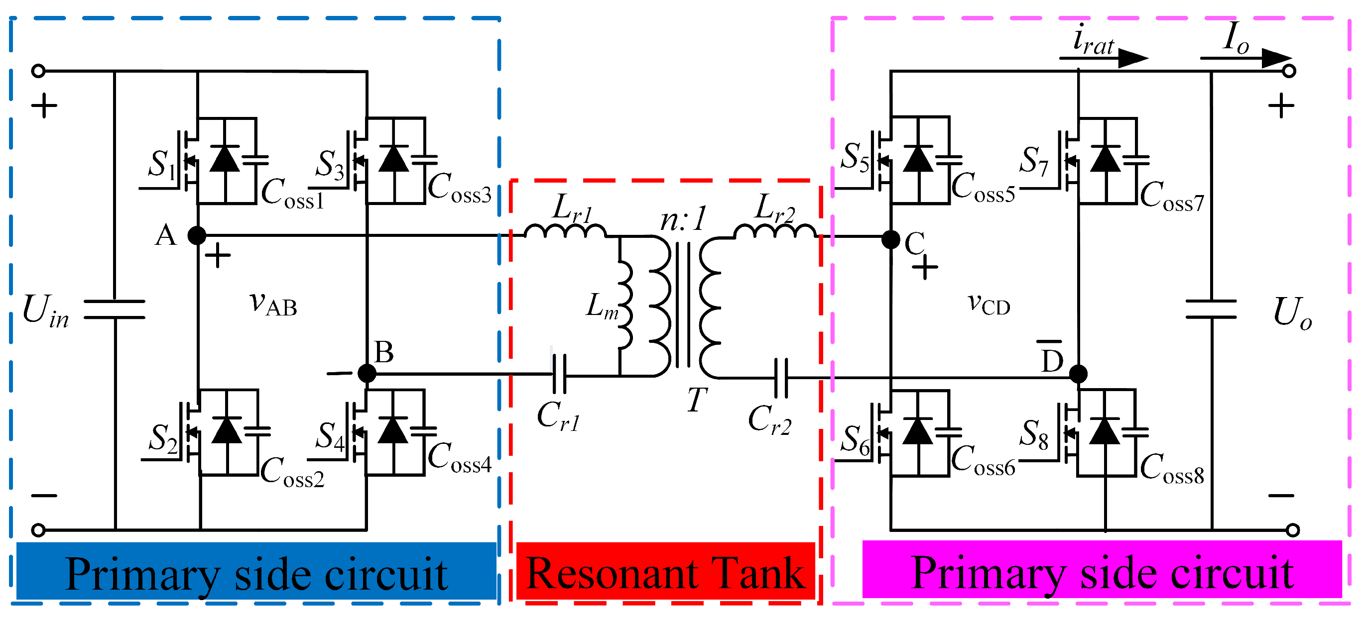
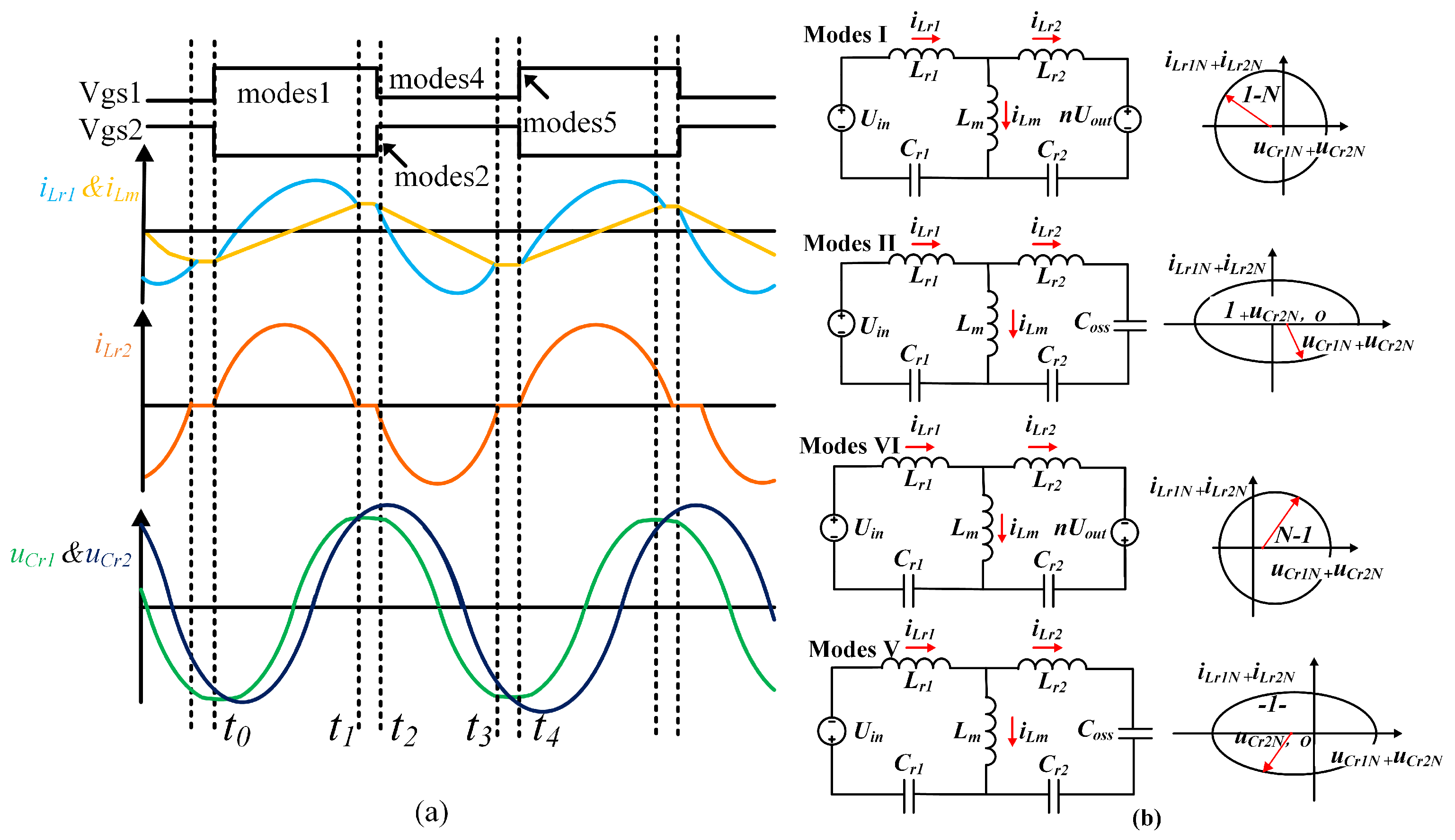
2. The SR Process for CLLC Resonant Converter

The topology of the CLLC resonant converter is shown in Figure 1. It consists of two H-bridge circuits on the primary and secondary sides; the primary-side switching devices are denoted as S 1 S 4 , and the secondary-side switching devices are denoted as S 5 S 8 . The resonant tank is symmetrically distributed, and the resonant tank comprises resonant capacitors C r 1 , C r 2 , resonant inductors L r 1 , L r 2 , magnetizing inductors L m , and a transformer. The parameters of the resonant tank are designed symmetrically, following the specific relationship equations L r 1 = n 2 L r 2 , C r 1 = C r 2 n 2 . For simplicity, parasitic parameters are neglected in the subsequent modeling process.
In the driving of SR, several main issues arise: turning on too early or too late, and turning off too early or too late. As shown in Figure 2a,b, the late turn-on or early turn-off of the rectifier’s signal will cause the current on the secondary side to pass through the body diode of the MOSFET. While this does not affect the operation of the resonant converter, it results in additional conduction losses and reduced efficiency. As shown in Figure 2c,d, if the rectifier signal turns on early or turns off late, the load will be discharged, causing the output current to flow back to the rectifier in the reverse direction. This leads to energy transfer from the secondary side to the primary side, resulting in a large circulating current. As the circulating current continues to increase, the primary-side circuit may be damaged.

2.1. Below-Resonant State

Figure 3a shows the waveforms of the resonant converter operating in below-resonance mode, which is referred to as PO mode [25] in the literature. The time t 0 t 1 denotes the dead time of the MOSFET, and the optimal turn-on time of the synchronous rectifier gate signal is t 1 and the optimal turn-off time of the synchronous rectifier gate signal is t 2 . The primary resonant inductor current i L r 1 and the magnetizing inductor current i L m are equal during t 2 t 3 .
At the t 0 moment, the gate drive signal of S 2 and S 3 drops low. S 2 and S 3 turn OFF instantly if the C d s of the MOSFET is not taken into account. The inductor current of the primary side i L r 1 flows through the body diode of S 2 , S 3 . L r 1 , C r 1 , L m participate in resonance; the primary side ceases to transfer energy to the secondary side. L r 2 , C r 2 participate in resonance in this state. At moment t 1 , the L m stops resonating and is clamped at n U o .
At the t 1 moment, the primary switch tube S 1 , S 4 turns ON, and the rectifier tube S 5 , S 8 also turns ON simultaneously. At the t 2 moment, the current i L r l equals the current i L m , the resonant inductor is no longer clamped by the magnetizing inductor and participates in the resonance again, and all the secondary-side switches are turned OFF.
At the t 3 moment, the primary-side switching tube S 1 , S 4 turns OFF and continues to repeat the symmetrical half-switching cycle. In summary, the key to accurate SR in below resonance is accurately calculating the duty cycle D S R _ D u t y . The resonant frequency point can be considered a special below resonance, and SR can be implemented in the same manner as below-resonance SR.

2.2. Above-Resonant State

Figure 3b shows the critical waveforms for the over-resonant operation of the CLLC resonant converter. The optimal SR signal on and off times are when the resonant inductor current i L r l and the magnetizing inductor current i L m are twice equal. The key lies in calculating the delayed duty cycle D S R _ D e l a y of the rectifier tubes. The half-cycle states of the CLLC resonant converter are as follows.
At the t 0 moment, the drive signal of the primary-side switch S 2 , S 3 becomes zero and S 2 , S 3 is immediately turned off. Between t 0 and t 1 , the primary resonant current i L r l flows through the body diode S 1 , S 4 , the secondary-side current i r a t continues to be rectified, and the magnetizing inductor i L m is clamped.
At the t 1 moment, the primary-side switch over S 1 , S 4 turns off for dead-time, and the primary-side resonant inductor current i L r l flows through the drain-source channel S 1 , S 4 while the secondary-side current i r a t still flows through S 7 , S 8 for rectification.
At the t 2 moment, the primary-side resonant inductor current i L r l is equal to the excitation inductor current i L m . The rectifier tube S 6 , S 7 is disconnected and, after t 2 moments, the primary-side L r 1 , C r 1 forms a resonant network, the secondary-side L r 2 , C r 2 forms a resonant network, and the rectifier tube does not participate in the resonance.
Table 1 shows the state variables and normalization of the CLLC converter.

3. SR Method for CLLC Resonant Converters Based on State-Trajectory Models

It is obtained from the analysis of the Section 2 that the key to synchronous rectification is to calculate the timing of synchronous rectifier tubes in over-resonant and under-resonant states, and to propose a synchronous rectification strategy based on the state-trajectory model.

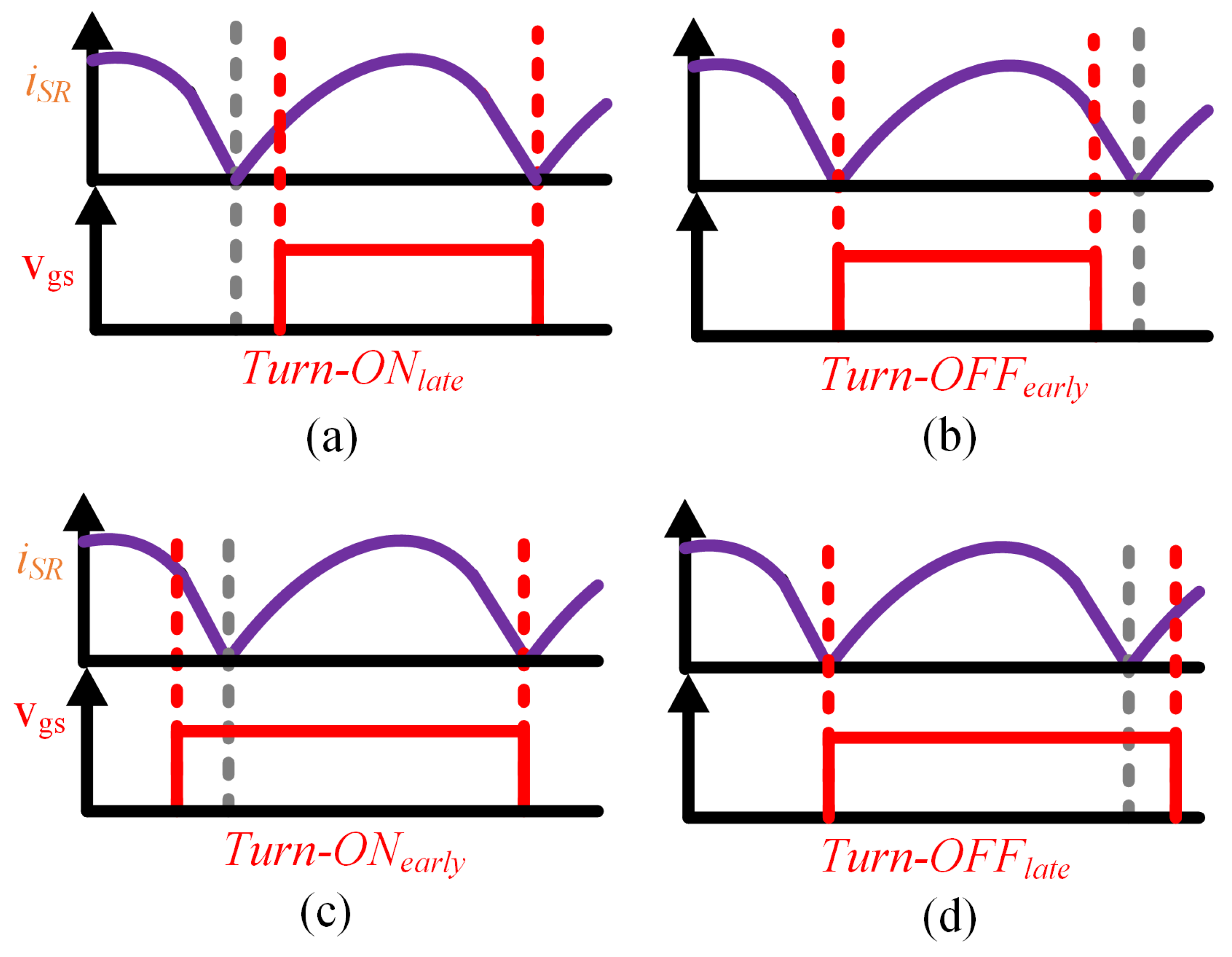
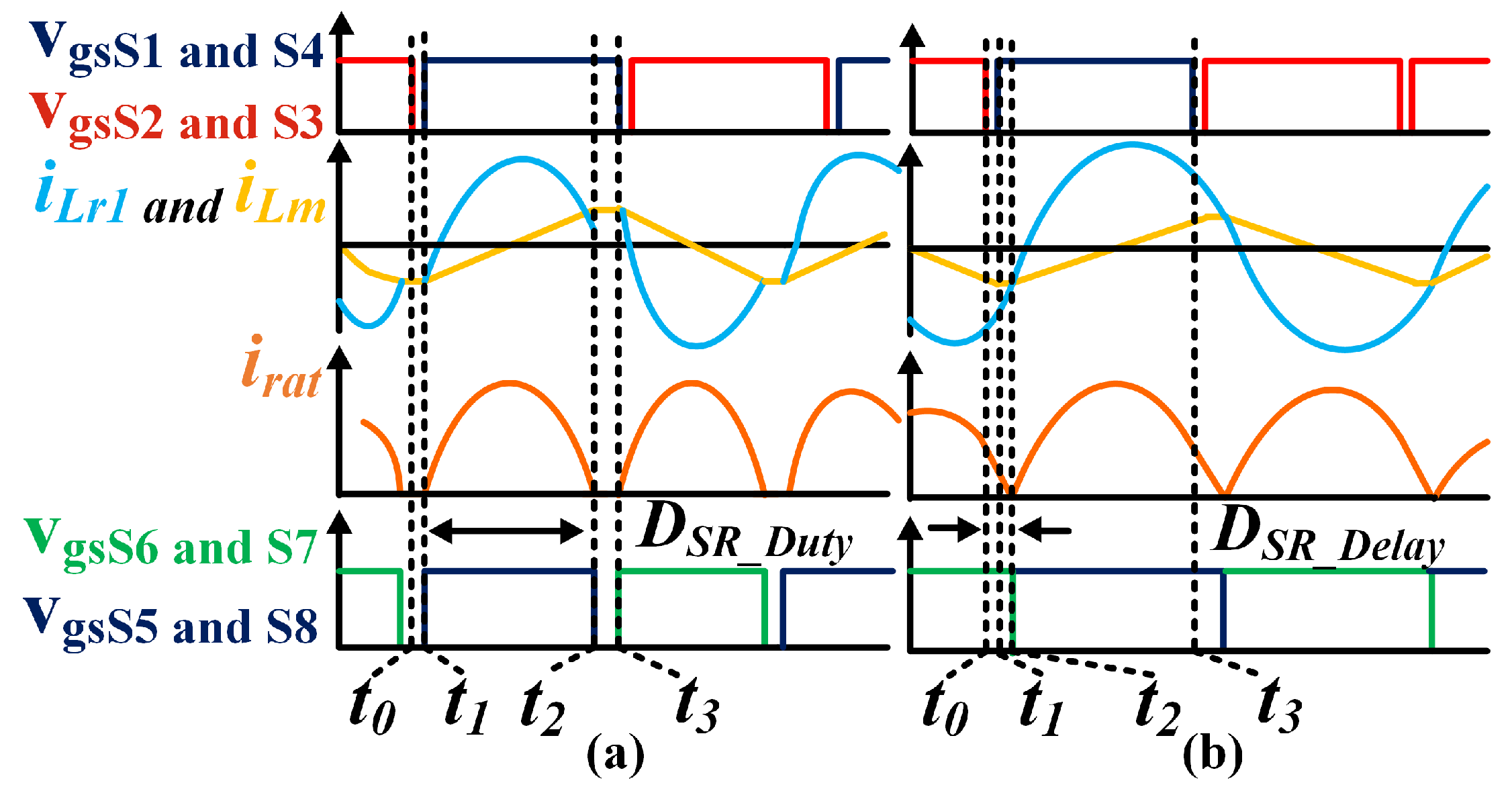
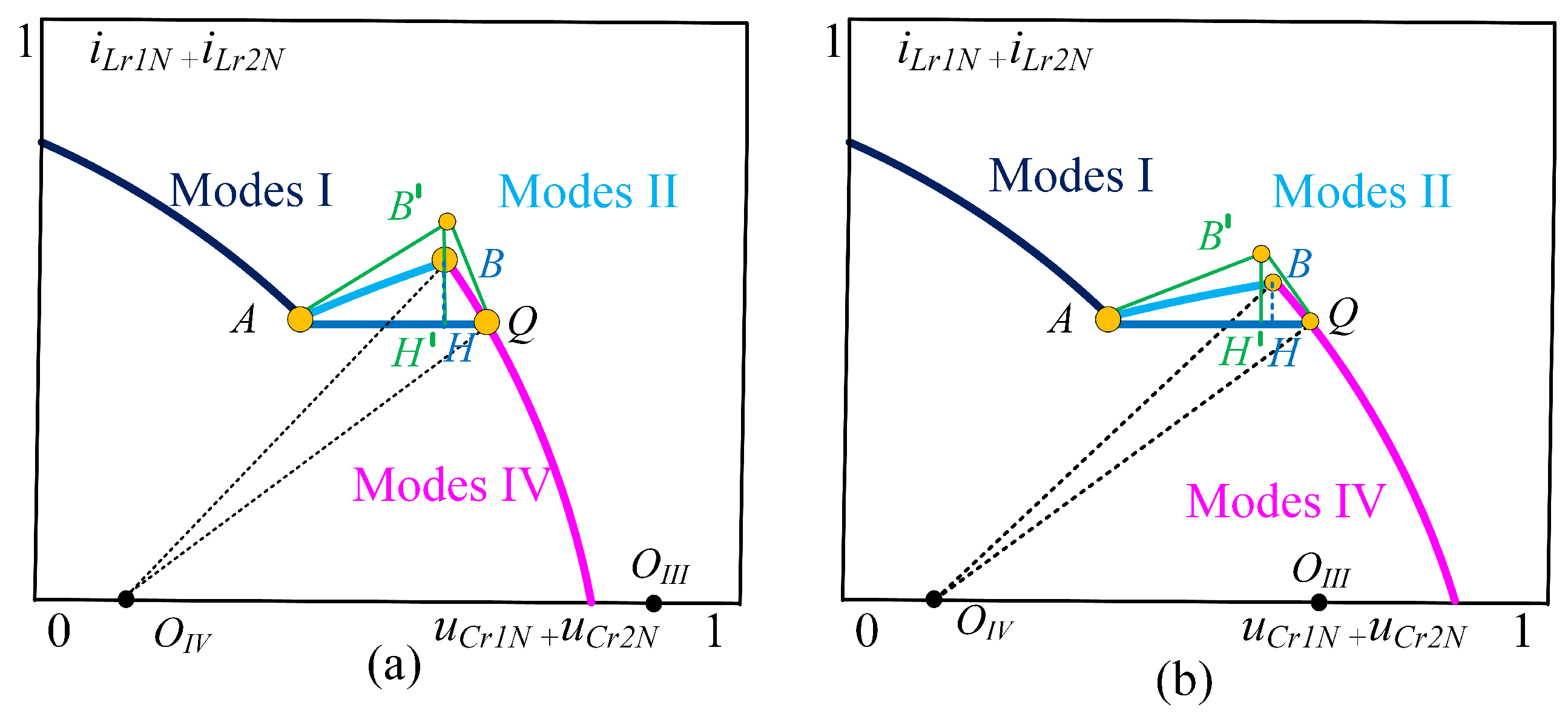
3.1. Above-Resonant Synchronous Rectification Method

Through the analysis in the Section 2, it can be seen that the resonant converter has a total of six modes. There are four modes in the over-resonant state—mode 1, mode 3, mode 4, and mode 6—as shown in Figure 4a for the modes corresponding to the middle of the key waveforms and Figure 4b for the trajectory diagrams and equivalent circuits corresponding to the four modes. The following expressions for the trajectories corresponding to the four modes are obtained from the KVL analysis circuit:
i L r 1 N ( t ) + i L r 2 N ( t ) 2 + u C r 1 N ( t ) + u C r 2 N ( t ) ( 1 N ) 2 = 4 P 1 2
i L r 1 N ( t ) + i L r 2 N ( t ) 2 + u C r 1 N ( t ) + u C r 2 N ( t ) ( 1 + N ) 2 = 4 P 1 2
i L r 1 N ( t ) + i L r 2 N ( t ) 2 + u C r 1 N ( t ) + u C r 2 N ( t ) ( 1 N ) 2 = 4 P 1 2
i L r 1 N ( t ) + i L r 2 N ( t ) and u C r 1 N ( t ) + u C r 2 N ( t ) are the sums of the resonant inductor currents and resonant capacitor voltages on the primary and secondary sides normalized to different modes, where the at-harmonic voltage gain is N = n U o u t U i n .
D S R _ D e l a y = θ I V / ω r
θ I V = θ 1 θ 2
θ 1 = arccos ( V C r 1 N _ E + V C r 2 N _ E ) x O I V R I V θ 2 = arccos ( V C r 1 N _ F + V C r 2 N _ F ) x O I V R I V
where θ I V is the angle of the center of the circle corresponding to the state IV, θ I V is as shown in Equation (6), and, according to the expression in Equation (7), it can be obtained that the final expression of θ I V is as follows:
θ I V = arccos ( V C r 1 N E + V C r 2 N E ) x O I V R I V arccos ( V C r 1 N F + V C r 2 N F ) x O I V R I V
where V C 1 N _ E + V C 2 N _ E and V C 1 N _ F + V C 2 N _ F are the sums of normalized resonant capacitance voltages C r 1 , C r 2 at the points E and F, respectively. Points E and F are the start and end points of mode 4, R I V is the radius corresponding to the pair of modes 4, O I V is the center of the circle of mode 4, and x O I V = 1 + N . Since points E and F are included in modes 1 and 4 and the CLLC resonant converter operates symmetrically for two half cycles, the following equations can be obtained by analyzing modes 1 and 4 and substituting points E, F, and H:
R I = ( i L r 1 N E + i L r 2 N E ) 2 + [ u C r 1 N E + u C r 2 N E ( 1 N ) ] 2 R I V = ( i L r 1 N E + i L r 2 N E ) 2 + [ u C r 1 N E + u C r 2 N E ( 1 + N ) ] 2 R I = ( i L r 1 N H + i L r 2 N H ) 2 + [ u C r 1 N H + u C r 2 N H ( 1 N ) ] 2 R I V = ( i L r 1 N F + i L r 2 N F ) 2 + [ u C r 1 N F + u C r 2 N F + ( 1 + N ) ] 2
In Equation (9), in which u C r 1 N E + u C r 2 N E , u C r 1 N H + u C r 2 N H , and u C r 1 N F + u C r 2 N F correspond to the sum of the resonant capacitor u C r 1 N F + u C r 2 N F voltages for modes E, F, and H, and i L r 1 N E + i L r 2 N E , i L r 1 N H + i L r 2 N H , and i L r 1 N F + i L r 2 N F correspond to the sum of the resonant capacitor i L r 1 , i L r 2 currents for modes E, F, and H, R I is the radius of the mode 1 trajectory, and R I V is the radius of the trajectory of mode 4.
n U o u t N = ( u C r 1 N E + u C r 2 N E ) / ( u C r 1 N F + u C r 2 N F )
Next, the output current I o u t N is determined by solving, and the output current can be solved by the difference between the primary resonant inductor current i L r 1 N and the excitation inductor current i L m N :
I outN = f N π t s | i L rN i L mN | d t
Half of the cycle consists of mode 1 and mode 4, where L m is clamped in a voltage of magnitude n U o u t . The other half of the state consists of mode 3 and mode 5, where L m is clamped in a voltage of magnitude n U o u t . According to the principle of volt-second equilibrium, one can be derived as follows:
i L mN = ( t t 1 t s / 4 ) n Z 1 U outN L m
By taking (12) into (11), it can be derived as follows:
I outN = f N π t 1 t 3 | i L rN i L mN | d t = f N π [ ( u Cr 1 N E u Cr 1 N G ) + ( Cr 1 N F u Cr 1 N E ) ] = 2 f N π u Cr 1 N F
As shown in Figure 5, the resonant capacitors C r 1 and C r 2 have equal voltages at the time indicated in the figure, corresponding to the points in the trajectory diagram. Therefore, the following relationship can be derived:
u Cr 1 N F + u Cr 2 N F = I o u t N π / f N
By taking (14) into (11), it can be obtained as follows:
u C r 1 N E + u C r 2 N E = n U o u t N I o u t N π / f N
From Figure 5, i L r 1 N and i L m N are equal at times t 0 and t 2 , so the voltage difference i L r 2 N is zero at these two time points. Therefore, from Equation (12), the following relationship can be derived:
i L r 1 N F = n Z 1 U outN 4 f s L m
The delayed duty cycle of the synchronous rectifier gate signal in the over-resonant state can be obtained by substituting Equations (14)–(16) into Equation (8):
D S R _ D e l a y = ( arccos n U o u t N I o u t N π / f N + ( 1 + N ) I o u t N π / f N + 1 + N 2 + n Z 1 U o u t N / ( 4 f s L m ) 2 arccos I o u t N π / f N + ( 1 + N ) I o u t N π / f N + 1 + N 2 + n Z 1 U o u t N / ( 4 f s L m ) 2 ) / ( 1 L r 1 C r 1 )

3.2. SR Method in the Below-Resonance Region

There are four modes in the below-resonant state: mode 1, mode 2, mode 4, and mode 5. As shown in Figure 6a, the key waveforms corresponding to these modes are illustrated, while Figure 6b presents the trajectory diagrams and equivalent circuits for the four modes.
i L r 1 N ( t ) + i L r 2 N ( t ) k 2 2 + u C r 1 N ( t ) + u C r 2 N ( t ) ( 1 + u C r 2 N , O ) 2 = I 1 O k 2 2
I ˙ L r 1 N ( t ) + I ˙ L r 2 N ( t ) k 2 2 + u C r 1 N ( t ) + u C r 2 N ( t ) ( 1 u C r 2 N , O ) 2 = I 1 O k 2 2
where k 2 = k + 1 , I 1 O are quantities related to the initial state of the circuit.
It is straightforward in the literature to simplify the two segments AB and CD by arguing that, in the case of L m L r 1 , where AB and CD are constant in the case of modes 2 and 5, these two segments can be thought of as the two segments CP and AQ. Thus, the duration of i L r 1 N A + i L r 2 N A = i L r 1 N Q + i L r 2 N Q , i L r 1 N C + i L r 2 N C = i L r 1 N P + i L r 2 N P and mode 1 is half the period and is no longer related to the voltage gain and load.
Figure 7 shows an enlarged view of the state trajectory of mode 2 of the CLLC resonant converter. From this figure, it can be observed that the exact trajectory of mode 2 is not linear. If the duration of mode 1 and mode 4 is t r / 2 , then BR in mode 4 becomes redundant. Therefore, based on the analysis according to Figure 8, a relatively large error occurs when performing synchronous rectification. Due to the symmetry of the operating state of the resonant converter, it is only necessary to analyze half a cycle, focusing on mode 2 and mode 4. The duty cycle of the synchronous rectified signal is derived as follows:
D S R _ D u t y = 0.5 t I I f s
Equation (21) Δ u C r 1 N _ A B is the sum of the resonant capacitor voltage difference between the two points AB. i L r 1 N I I is the resonant inductor current because, in the period t I I , the secondary resonant current i L r 2 N I I is zero, so t I I is calculated only by the primary resonant inductor current and the voltage of the resonant capacitor. Because AB is a circular arc, the process is very complicated in solving for the u C r 1 N A B time. To simplify the solution process, the tangent lines of modes 2 and 4 are constructed using geometrical methods and solved within the triangle. The tangents of modes 2 and 4 intersect at a point B ; as shown in Figure 7a, the perpendiculars B H and BH from AB are drawn and almost coincident, proving that the errors of B H and BH are minimal. This Δ U C r 1 N A B can be expressed as Δ U C r 1 N A B , which follows from the tangent principle:
Δ u C r 1 N _ A B = k R _ I V Δ u C r 1 _ A Q / ( k Q _ I V + k A _ I I )
k R _ I V and k R _ I I in (21) are the slopes of A B and R B , respectively, and k R _ I V , k R _ I I can be obtained by substituting the coordinates of point A and point B into (3) and (17).
k A I I = Z 1 Z 2 × u Cr 1 N _ A + 1 i L r 1 N _ A
k R _ IV = Z 1 Z 2 × u Cr 1 N _ Q + u Cr 2 N _ Q + n U o u t N + 1 i L r 1 N _ Q + i L r 2 N _ Q
where u Cr 1 N _ A and u Cr 1 N _ Q are the normalized resonant capacitor voltages at points A and B.
As shown in Figure 7b, as the output voltage and load increase, point A will reach the right side of the vertex of the mode 2 trajectory, x O I I = 1 . It is no longer accurate to continue to view mode 2 simply as a tangent to point A to facilitate the simulation of the trajectory of mode 2. Instead of k A _ I I , the weighted slope of mode 2, k I I is introduced in (21), and its expression is given by the following:
k II = k A _ I I 1 u Cr 1 N _ A + k Q _ II 1 u Cr 1 N _ Q u Cr 2 N _ Q Δ u Cr 1 N _ AQ + Δ u Cr 2 N _ AQ
where A is the imaginary slope of mode 2 at point B, which can be derived as follows:
k Q ⨿ = Z 1 Z 2 × u Cr 1 N Q + u Cr 2 N Q 1 i Lr 1 N Q + i Lr 2 N Q
It follows from (22)–(25) above that the variables involved are u Cr 1 N _ Q + u Cr 2 N _ Q , i Lr 1 N _ Q + i Lr 2 N _ Q , u Cr 1 N _ A , and i L r 1 N _ A , which can be calculated by clamping the voltage:
i L r 1 N _ R = i L r 1 N _ A = i L m N A = n Z 1 U o u t N / 4 f r L m
The trajectory radius of mode 1 can be expressed as follows:
R I = i L mN 2 + i ratN 2
In Equation (27), i L m N equals i L r 1 N _ A and i L m N is the maximum current of the excitation inductor. Since the output current I O N is the average of the rectifier current i r a t N , and assuming that i r a t N is a sinusoidal waveform, the I O N in the lower resonance region is as follows:
I outN = f N π ʃ t s i ratN d t = f N π ʃ t s i ratN sin ( ω r t ) d t = 2 f N I ratN / π
The following is available:
u Cr 1 N _ A = I ratN + x OI = 0.5 I oN π / f N + 1 n V oN
Since AB is parallel to the x-axis, the difference between points A and B is equal to the center distance between mode 1 and mode 4; this can be obtained as follows:
Since A is parallel to the x-axis, the difference between point A and B is equal to the center distance between mode 1 and mode 4, and b denotes the voltage difference between the AB segments. From Equations (18) and (19), we can obtain the coordinates of the circle centers of mode 1 and mode 4: mode 1 center O I : ( 1 N , 0 ) , and mode 4 center O I V : ( 1 N , 0 ) , and the voltage difference is equal to the horizontal distance between the center of the circle, which is therefore obtained as follows:
Δ U C r 1 N A R = 2 n U o N 2
The process of point P to R corresponds to the transition from mode 4 to mode 2, and, according to the symmetry of the state trajectory, u C r N P = u C r N Q (Q is a symmetry point). From Equation (30), the voltage at point R increases by Δ u Cr 1 N A B compared to point P . Substitute the circular center position correction term for mode 2, 1 u Cr 2 N in Equation (19). The following is available:
V CrN _ R = V CrN _ P + 2 n V oN 2
The slope of the tangent line at point A is based on the mode 2 trajectory equation Equation (19). Derive Equation (19) and substitute the coordinates of point A : ( i Lr 1 N A , u Cr 1 N A ) . Combine the current/voltage expressions of Equations (26) and (29), the mode 4 trajectory radius R I V versus the output current, Equations (14)–(16). Utilizing the property that point R is on the rightmost side of the mode 4 trajectory i Lr 1 N R = 0 , eventually, the following can be obtained:
k A _ I I = k π I ON 2 n 2 U ON f N π ( 1 + k ) n 2 U ON f N k R _ I V = 2 π k I ON n 2 U ON f N k R _ I I = k π I ON + 2 n 2 + n U ON f N π ( 1 + k ) n 2 U ON f N
By taking (32) and (22) into (21), the following can be obtained:
D S R _ D u t y = 0.5 2 k I outN ( 1 + k ) [ 1 / ( n U outN ) + 1 ] π [ 4 n + I outN ( 1 + k ) π / f N ]

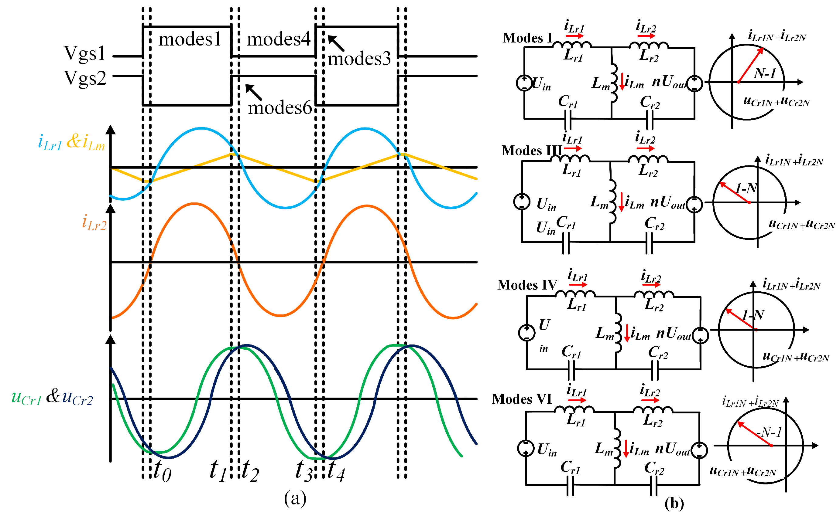
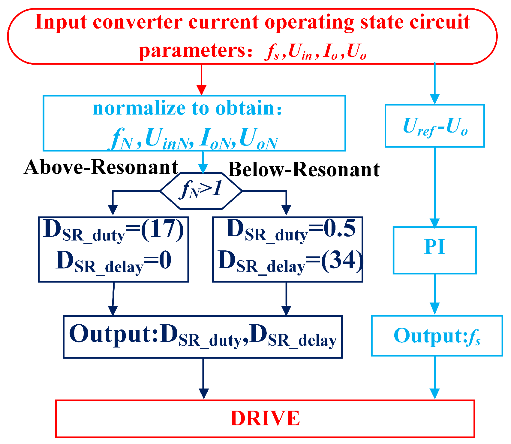
3.3. SR Strategy Based on State Trajectories

In this paper, we propose a synchronous rectification method based on the gate signal delay duty cycle and the switching duty cycle calculated above.
Due to the difference between the synchronous rectification strategies for the over-resonant state and the under-resonant state, it is necessary to determine whether the system is in an over-resonant or under-resonant state based on the normalized switching frequency.
The duty cycle of the synchronous rectifier signal is selected according to the determined resonant state, as defined by Equation (5) or Equation (32).
Therefore, the synchronous rectification signal only requires sampling the input voltage, output voltage, and output current, eliminating the need for additional sampling circuits. This enables the dynamic real-time synchronization of the circuit state. The flowchart of the proposed synchronous rectification scheme for the CLLC resonant converter is illustrated in Figure 9. The CLLC resonant converter employs closed-loop control based on the voltage difference, and the control block diagram is presented in Figure 10.

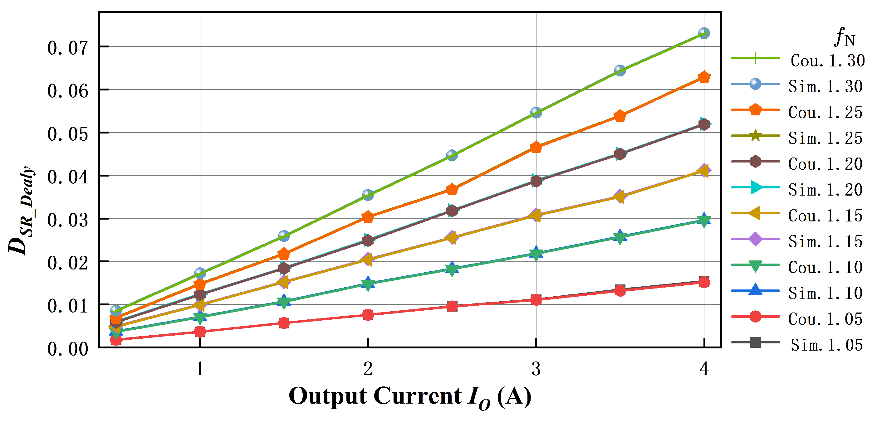
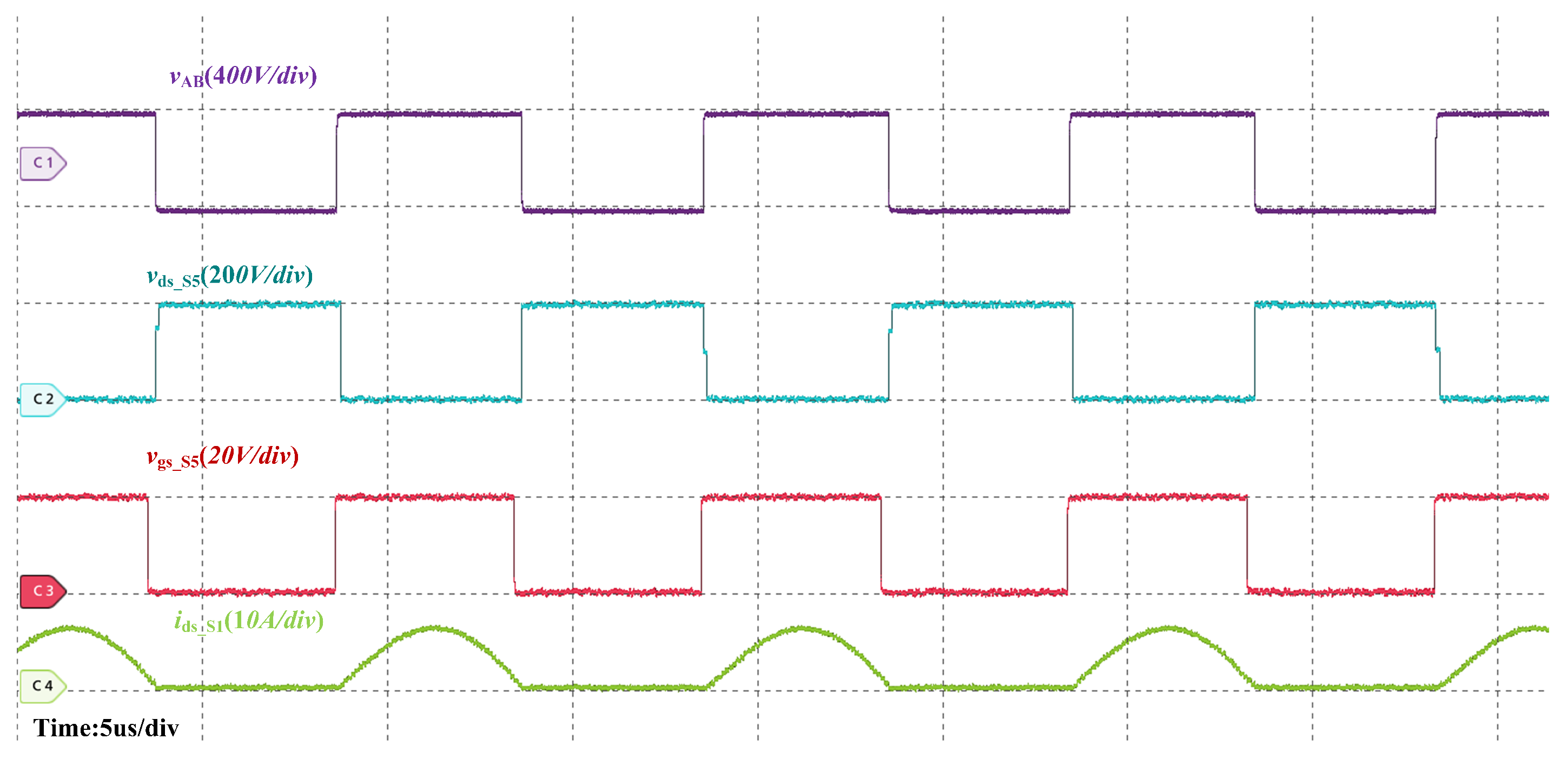
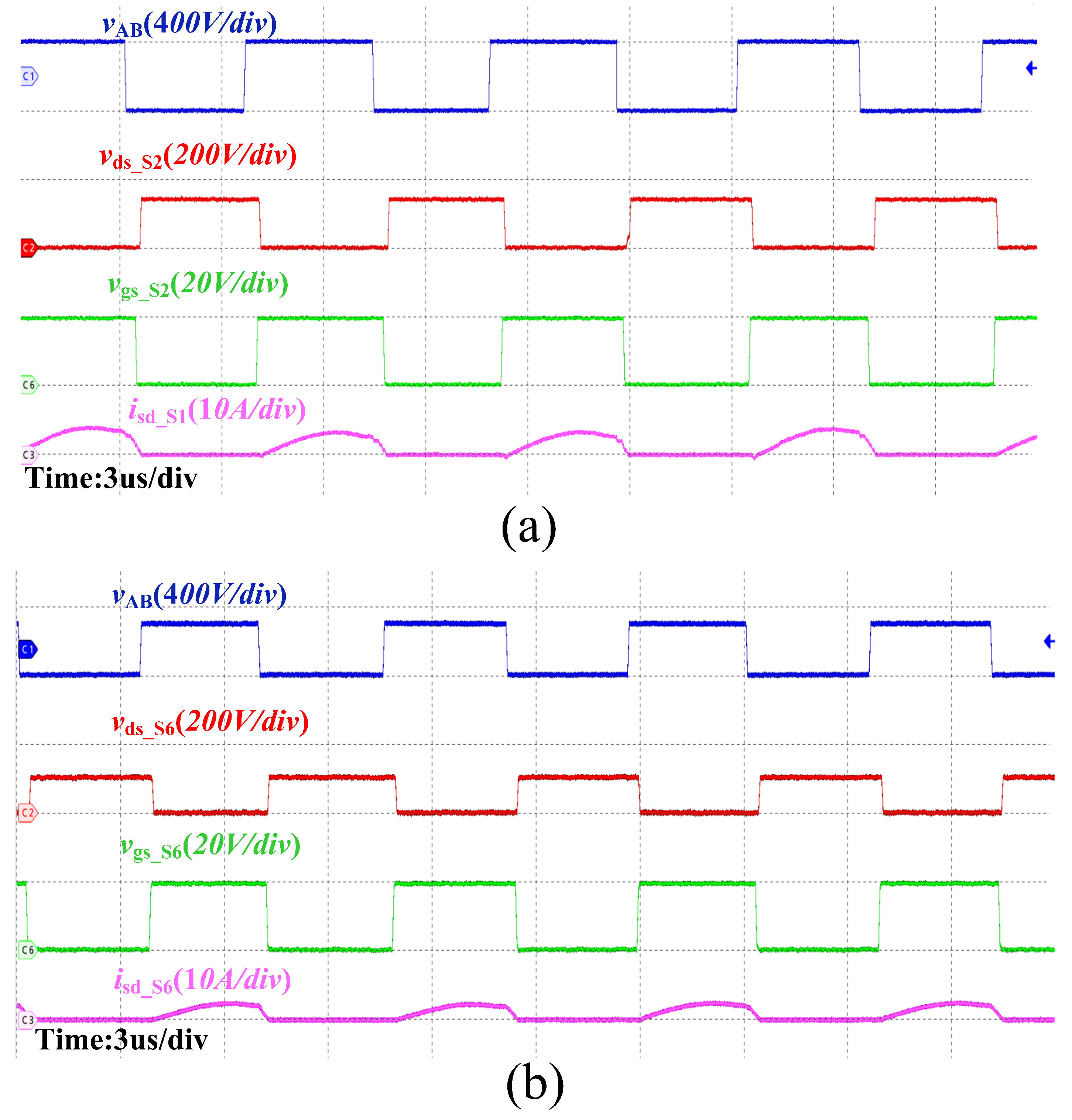
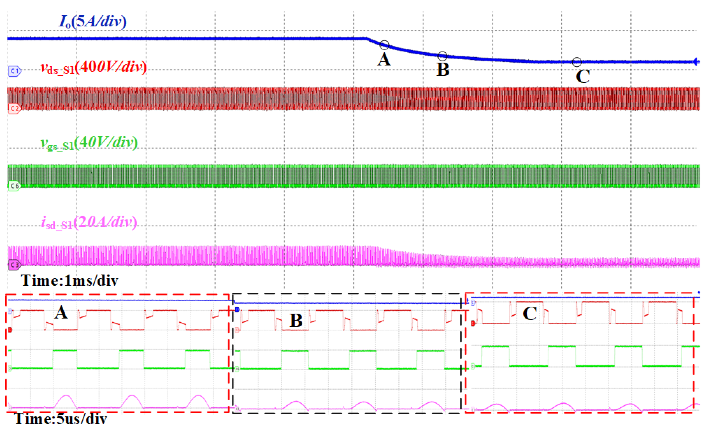
3.4. Simulation Verification
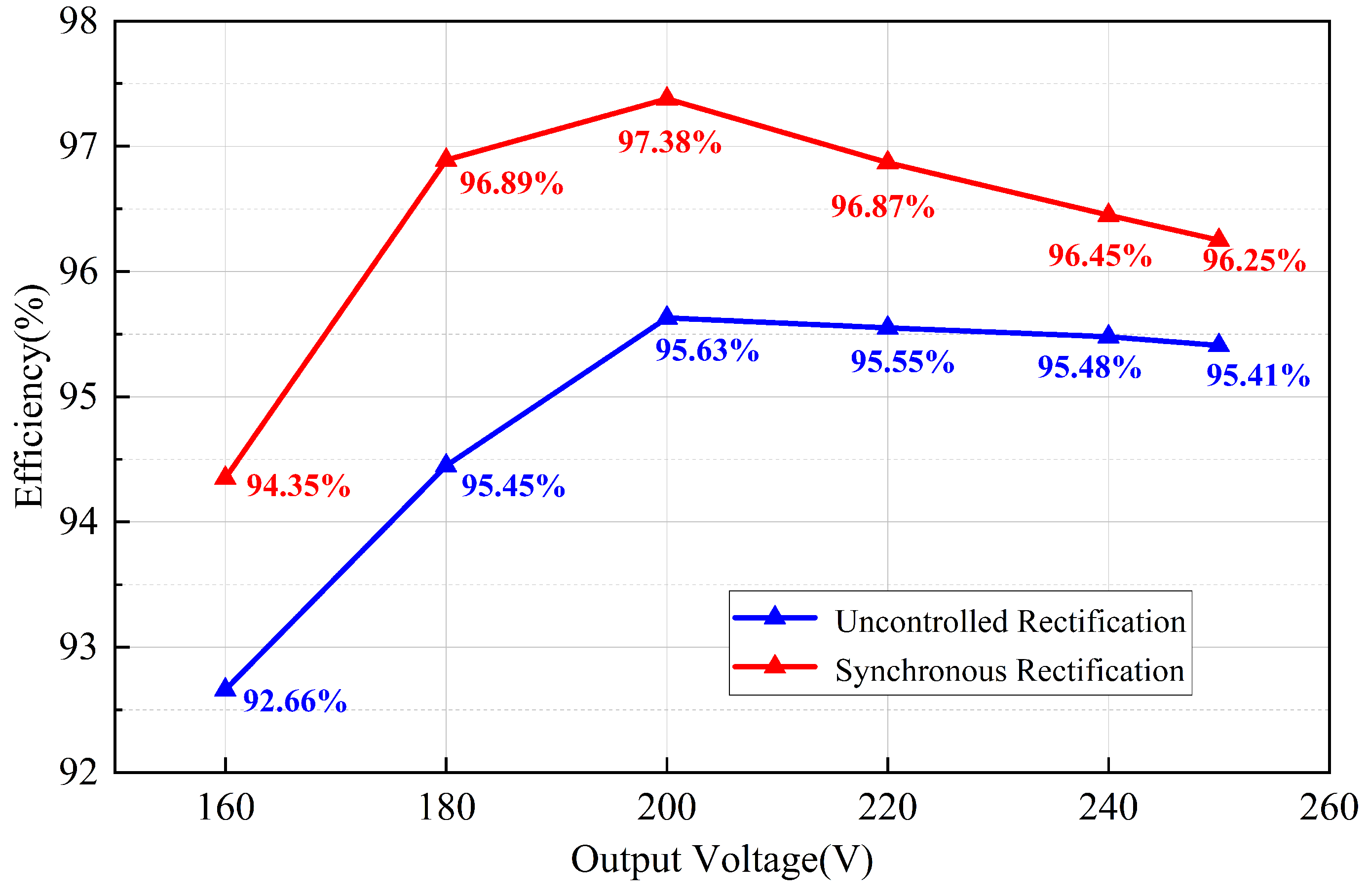
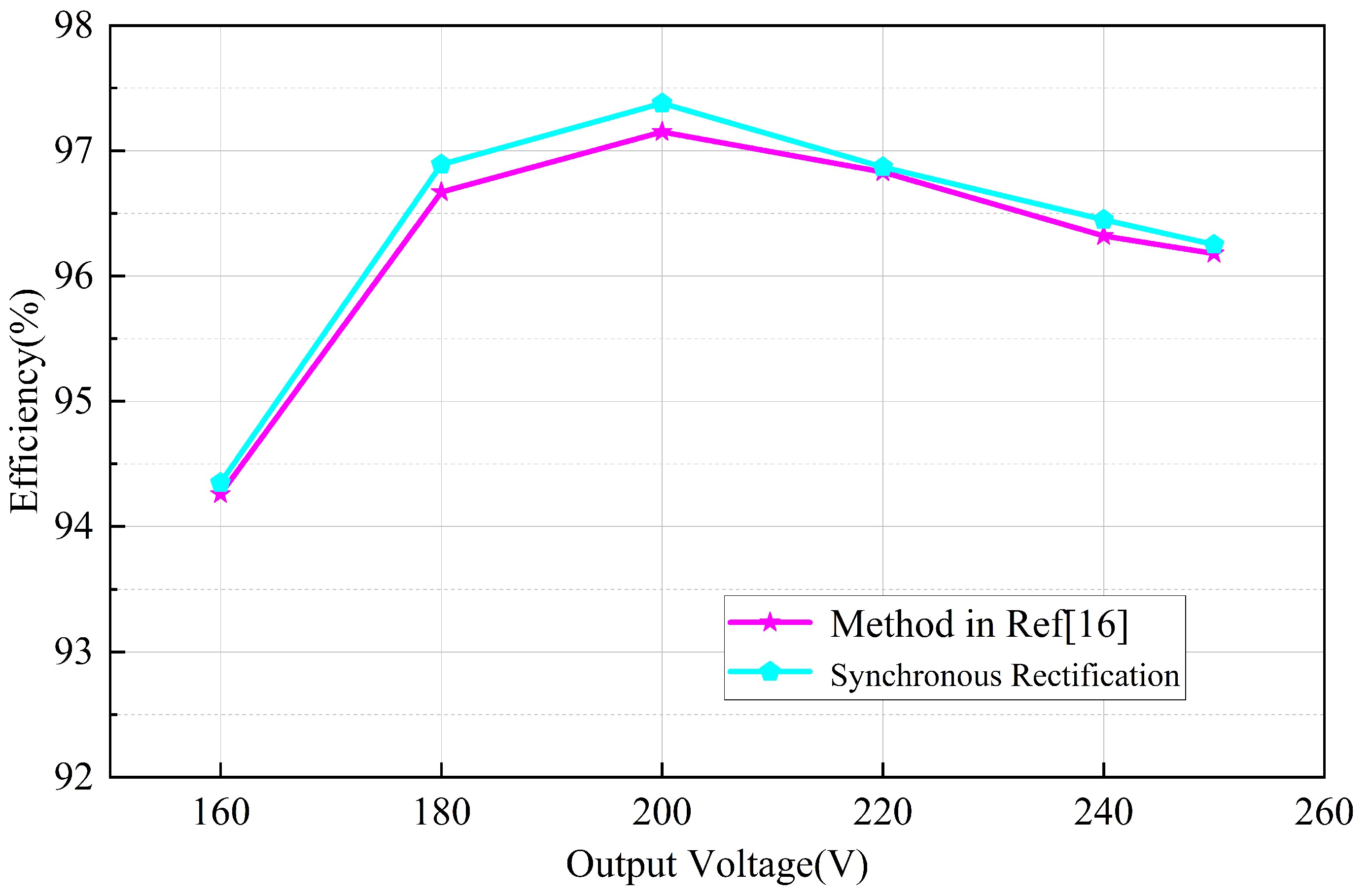
Compare the error between the simulation results and the calculated results, and contrast the synchronous rectification scheme under other modeling methods with the proposed method in this paper to verify the feasibility and accuracy of the proposed approach.
As shown in Figure 11, the delay duty cycle calculation results of the proposed synchronous rectification method are compared with the simulation results. It can be observed that the proposed calculation results exhibit high accuracy, with only a minor error between the calculated and simulated values.
As shown in Figure 12, the duty cycle calculation results of the proposed synchronous rectification method are compared with the simulation results. It can be observed from the figure that the proposed method maintains high accuracy over a wide range of current and frequency variations. Although the error in the over-resonant region is slightly larger, with a maximum error of 1.7%, the impact on the simulation results is minimal due to the relatively large value of the duty cycle itself. This demonstrates the high accuracy of the proposed method.
The small error between the calculated and simulated results in Figure 12 arises from the simplified geometric approximations used in the state-trajectory model, particularly in the below-resonance region. While these approximations reduce the computational complexity, they introduce minor deviations from the exact nonlinear behavior of the resonant converter. The error remains within an acceptable range (max 1.7%) and has a negligible impact on the overall performance.

4. Discussion

To verify the feasibility of the proposed synchronous rectification scheme for the CLLC resonant converter, an 800 W experimental prototype was constructed. The experimental setup is illustrated in Figure 13, with the topology identical to that shown in Figure 1. The parameters of the experimental prototype are detailed in Table 2.
The switching signals for the proposed SR method were generated using a digital signal processor (DSP, TMS320F28335), which dynamically calculates the optimal turn-on/off timing based on real-time measurements of the input voltage, output voltage, and current.

Verification of Accuracy

Figure 14 shows the main waveforms of the converter at an input voltage of 200 V and an output voltage of 200 V, operating at the resonance point. As can be seen from the figure, the synchronous rectifier signal is consistent with the ideal conduction state. There is no premature shutdown or advance conduction of the rectifier, which proves the accuracy and effectiveness of the present method at the resonance point.
To verify the accuracy of the synchronous rectification scheme in both forward and reverse directions under under-resonance and over-resonance states, the CLLC resonant converter was operated in a resonant state. The forward and reverse operations of the CLLC resonant converter were validated. Figure 15a illustrates the key waveforms of the converter in forward operation with an input voltage of 200 V and an output voltage of 250 V. Figure 15b depicts the key waveforms of the converter in reverse operation with an input voltage of 250 V and an output voltage of 300 V.
Figure 16a presents the key waveforms of the converter in under-resonant mode during forward operation with an input voltage of 200 V and an output voltage of 160 V. Figure 16b shows the key waveforms of reverse operation in under-resonant mode, with an input voltage of 160 V and an output voltage of 130 V. From the above waveforms, it can be observed that the synchronous rectifier signal aligns with the ideal conduction state. There is no instance of the rectifier tube shutting down prematurely or conducting ahead of time, which confirms the accuracy of the proposed method.
Figure 17 illustrates the dynamic waveform of the switching current during forward operation in the under-resonant state, with an output voltage of 250 V and an output current changing from 4 A to 1 A. The figure demonstrates that the proposed synchronous rectification scheme exhibits excellent dynamic performance in the under-resonant state.
Figure 18 depicts the dynamic waveform of the switching current during forward operation in the over-resonant state, with an output voltage of 160 V and an output current changing from 3.5 A to 1 A. From the figure, it can be observed that the over-resonant state also demonstrates a good dynamic performance. However, a slight error in the over-resonant state may lead to a minor degradation in the rectifier performance. Nevertheless, the proposed synchronous rectification scheme maintains high dynamic performance and accuracy.
As shown in Table 3, the proposed SR method is compared with other SR methods reported in the literature. The proposed method achieves accurate synchronous rectification with low complexity, broader applicability, and without the need for additional auxiliary circuits or sensors.
As shown in Figure 19, the proposed SR method significantly enhances the overall operating efficiency of the CLLC resonant converter.
Figure 20 compares the efficiency of the proposed synchronous rectification scheme with the SR scheme reported in the literature [16] and the conventional model-based approach. It can be observed that the proposed method achieves higher efficiency compared to the technique described in [16]. This improvement in efficiency is attributed to the higher accuracy of the proposed method, resulting in a significantly smaller computed SR timing error.

5. Conclusions

In this paper, a state-trajectory model is introduced into the CLLC resonant converter, and a novel synchronous rectification (SR) strategy specifically designed for the CLLC resonant converter is proposed. The proposed SR strategy requires only the detection of the input voltage, output voltage, and output current, eliminating the need for additional auxiliary circuits. To validate the effectiveness of the proposed strategy, an 800 W converter prototype was constructed and experimentally tested. The results demonstrate that the proposed SR algorithm achieves high accuracy across a wide range of operating conditions, including both steady-state and dynamic processes. Compared to uncontrolled rectification, the proposed synchronous rectification method significantly improves efficiency, with a rated efficiency of 97.38%. Overall, the proposed method exhibits high accuracy and efficiency, providing an effective solution for the performance optimization of CLLC resonant converters. Future work could explore the adaptability of this method to asymmetric CLLC topologies and AI-based real-time state-trajectory prediction to enhance its application potential under dynamic operating conditions.

Author Contributions

Conceptualization, Z.S.; methodology, C.F.; methodology, Q.Y.; software, C.R.; writing—original draft preparation, T.Z. All authors have read and agreed to the published version of the manuscript.

Funding

This research received no external funding.

Institutional Review Board Statement

Not applicable.

Informed Consent Statement

Not applicable.

Data Availability Statement

The original contributions presented in this study are included in the article.

Conflicts of Interest

The authors declare no conflicts of interest.

References

  1. Sun, J.; Yuan, L.; Gu, Q.; Duan, R.; Lu, Z.; Zhao, Z. Design-Oriented Comprehensive Time-Domain Model for CLLC Class Isolated Bidirectional DC-DC Converter for Various Operation Modes. IEEE Trans. Power Electron. 2020, 35, 3491–3505. [Google Scholar] [CrossRef]
  2. Jung, J.-H.; Kim, H.-S.; Ryu, M.-H.; Baek, J.-W. Design Methodology of Bidirectional CLLC Resonant Converter for High-Frequency Isolation of DC Distribution Systems. IEEE Trans. Power Electron. 2013, 28, 1741–1755. [Google Scholar] [CrossRef]
  3. Zahid, Z.U.; Dalala, Z.M.; Chen, R.; Chen, B.; Lai, J.-S. Design of Bidirectional DC–DC Resonant Converter for Vehicle-to-Grid (V2G) Applications. IEEE Trans. Transp. Electrif. 2015, 1, 232–244. [Google Scholar] [CrossRef]
  4. Li, B.; Jing, L.; Wang, X.; Chen, N.; Liu, B.; Chen, M. A Smooth Mode-Switching Strategy for Bidirectional OBC Base on V2G Technology. In Proceedings of the 2019 IEEE Applied Power Electronics Conference and Exposition (APEC), Anaheim, CA, USA, 17–21 March 2019. [Google Scholar]
  5. Rojas-Dueñas, G.; Riba, J.-R.; Moreno-Eguilaz, M. A Deep Learning-Based Modeling of a 270 V-to-28 V DC-DC Converter Used in More Electric Aircrafts. IEEE Trans. Power Electron. 2022, 37, 509–518. [Google Scholar] [CrossRef]
  6. Emamalipour, R.; Lam, J. A Multi-Mode Full-Bridge/Modified-Stacked-Switches Structured CLLC Resonant Converter for Energy Storage Applications. IEEE Trans. Power Electron. 2024, 39, 5967–5981. [Google Scholar] [CrossRef]
  7. Ravariu, C. Vacuum Nano-Triode in Nothing-On-Insulator Configuration Working in Terahertz Domain. IEEE J. Electron Devices Soc. 2018, 6, 1115–1123. [Google Scholar] [CrossRef]
  8. Pei, L.; Jia, L.; Wang, L.; Zhao, L.; Cao, W.; Zhu, L.; Pei, Y. Accurate Extraction of Body-Diode-Conduction for Synchronous Rectification of CLLC Resonant Converters in High-Voltage Application. IEEE Trans. Power Electron. 2024, 39, 5009–5013. [Google Scholar] [CrossRef]
  9. Zhang, Z.; Liu, C.; Si, Y.; Liu, Y.; Lei, Q. Investigation of Adaptive Synchronous Rectifier (SR) Driving Scheme for LLC/CLLC Resonant Converter in EV On-Board Chargers. In Proceedings of the 2020 IEEE Applied Power Electronics Conference and Exposition (APEC), New Orleans, LA, USA, 15–19 March 2020; pp. 2185–2191. [Google Scholar] [CrossRef]
  10. Chen, N.; Chen, M.; Li, B.; Wang, X.; Sun, X.; Zhang, D.; Jiang, F.; Han, J. Synchronous Rectification Based on Resonant Inductor Voltage for CLLC Bidirectional Converter. IEEE Trans. Power Electron. 2022, 37, 547–561. [Google Scholar] [CrossRef]
  11. Chen, M.; Zhang, D.; Chen, N.; Li, B.; Wang, X.; Sun, X.; Jiang, F. A Coupled Inductor Scheme for CLLC Bidirectional Converter and Optimized Current Detection Method. IEEE Trans. Power Electron. 2022, 37, 11546–11551. [Google Scholar] [CrossRef]
  12. Schobre, T.; Siebke, K.; Mallwitz, R. Design of a GaN based CLLC converter with synchronous rectification for on-board vehicle charger. In Proceedings of the PCIM Europe 2019, International Exhibition and Conference for Power Electronics, Intelligent Motion, Renewable Energy and Energy Management, Nuremberg, Germany, 7–9 May 2019; pp. 1–5. [Google Scholar]
  13. Schobre, T.; Siebke, K.; Mallwitz, R. Operation Analysis and Implementation of a GaN Based Bidirectional CLLC Converter with Synchronous Rectification. In Proceedings of the 2019 21st European Conference on Power Electronics and Applications (EPE ’19 ECCE Europe), Genova, Italy, 2–5 September 2019; pp. P.1–P.10. [Google Scholar] [CrossRef]
  14. Zou, S.; Lu, J.; Mallik, A.; Khaligh, A. 3.3 kW CLLC converter with synchronous rectification for plug-in electric vehicles. In Proceedings of the 2017 IEEE Industry Applications Society Annual Meeting, Cincinnati, OH, USA, 1–5 October 2017; pp. 1–6. [Google Scholar] [CrossRef]
  15. Zou, S.; Lu, J.; Mallik, A.; Khaligh, A. Bi-Directional CLLC Converter with Synchronous Rectification for Plug-In Electric Vehicles. IEEE Trans. Ind. Appl. 2018, 54, 998–1005. [Google Scholar] [CrossRef]
  16. Sankar, A.; Mallik, A.; Khaligh, A. Extended Harmonics Based Phase Tracking for Synchronous Rectification in CLLC Converters. IEEE Trans. Ind. Electron. 2019, 66, 6592–6603. [Google Scholar] [CrossRef]
  17. Li, B.; Chen, M.; Wang, X.; Chen, N.; Sun, X.; Zhang, D. An Optimized Digital Synchronous Rectification Scheme Based on Time-Domain Model of Resonant CLLC Circuit. IEEE Trans. Power Electron. 2021, 36, 10933–10948. [Google Scholar] [CrossRef]
  18. Li, H.; Sun, Y.; Wang, S.; Zhang, Z.; Ren, X.; Zhang, P.; Yang, G.; Hu, C. Bidirectional Control with Fitting Model-Based Synchronous Rectification and Input Ripple Current Feedforward for SiC Bidirectional CLLC EV Charger. IEEE Trans. Ind. Electron. 2023, 70, 9136–9146. [Google Scholar] [CrossRef]
  19. Wang, Y.; Wang, F.; Zhuo, F.; Yu, K.; Tian, J.; Song, R. Analysis of High Performance Synchronous Rectified CLLC Resonant Converter with Reactive Power Optimization. IEEE Trans. Power Electron. 2023, 38, 15253–15271. [Google Scholar] [CrossRef]
  20. Wang, Y.; Wang, F.; Zhuo, F.; Yu, K.; Tian, J.; Zhang, X. Synchronous Rectification and Parameter Design Based on Accurate Time-Domain Model for Asymmetrical CLLC Resonant Converter. IEEE Trans. Transp. Electrif. 2025, 11, 4681–4697. [Google Scholar] [CrossRef]
  21. Pei, L.; Jia, L.; Wang, L.; Zhao, L.; Song, S.; Pei, Y.; Yang, X.; Gan, Y. A Time-Domain-Model-Based Digital Synchronous Rectification Algorithm for CLLC Resonant Converters Utilizing a Hybrid Modulation. IEEE Trans. Power Electron. 2022, 37, 2815–2829. [Google Scholar] [CrossRef]
  22. Chen, H.; Sun, K.; Shi, H.; Ha, J.I.; Lee, S. A Battery Charging Method With Natural Synchronous Rectification Features for Full-Bridge CLLC Converters. IEEE Trans. Power Electron. 2022, 37, 2139–2151. [Google Scholar] [CrossRef]
  23. Ren, X.; Pei, L.; Song, S.; Zhang, J.; Pei, Y.; Wang, L. A Digital Sensor-less Synchronous Rectification Algorithm for Symmetrical Bidirectional CLLC Resonant Converters. In Proceedings of the 2020 IEEE Applied Power Electronics Conference and Exposition (APEC), New Orleans, LA, USA, 15–19 March 2020; pp. 962–968. [Google Scholar] [CrossRef]
  24. Rezayati, M.; Tahami, F.; Schanen, J.-L.; Sarrazin, B. Generalized State-Plane Analysis of Bidirectional CLLC Resonant Converter. IEEE Trans. Power Electron. 2022, 37, 5773–5785. [Google Scholar] [CrossRef]
  25. Chen, H.; Wang, L.; Sun, K.; Lu, L. A Switching Delay Strategy for Sensorless Synchronous Rectification in CLLC Converters. IEEE Trans. Power Electron. 2024, 39, 280–293. [Google Scholar] [CrossRef]
Figure 1. Topology of the CLLC converter.
Applsci 15 04372 g001
Figure 2. Incorrect conduction of rectifier signals. (a) Late turn-on, (b) early turn-off, (c) early turn-on, (d) late turn-off.
Applsci 15 04372 g002
Figure 3. Key waveform of the LLC converter (a) in the above-resonance region and (b) in the below-resonance region.
Applsci 15 04372 g003
Figure 4. Plane trajectory of the above-resonant state. (a) Key waveforms in the above-resonant region. (b) Equivalent circuit corresponding to the state plane trajectory.
Applsci 15 04372 g004
Figure 5. Plane trajectory of the above-resonant state.
Applsci 15 04372 g005
Figure 6. Key waveforms and corresponding trajectories of the CLLC resonant converter. (a) Key waveforms in the below-resonant region. (b) Equivalent circuit corresponding to the state plane trajectory.
Applsci 15 04372 g006
Figure 7. III -state trajectory of CLLC converter amplification. (a) Q -point on the left side of O I I I . (b) Q -point on the right side of O I I I .
Applsci 15 04372 g007
Figure 8. Plane trajectory of the under-resonant state.
Applsci 15 04372 g008
Figure 9. Flowchart of the proposed synchronous rectification scheme.
Applsci 15 04372 g009
Figure 10. Closed-loop control block diagram.
Applsci 15 04372 g010
Figure 11. Closed-loop control block diagram. Comparison of the calculated and simulated results of the delayed duty cycle of the SR gate drive signal in the above-resonance region for the proposed synchronous rectification scheme is plotted.
Applsci 15 04372 g011
Figure 12. Comparison of calculated and simulated SR gate drive signal duty cycle in the below-resonant region for the proposed synchronous rectification scheme.
Applsci 15 04372 g012
Figure 13. Comparison of calculated and simulated SR gate drive signal duty cycle in the below-resonant region for the proposed synchronous rectification scheme.
Applsci 15 04372 g013
Figure 14. SR waveforms for forward operation of the CLLC resonant converter in the under-resonant state.
Applsci 15 04372 g014
Figure 15. SR waveforms for forward and reverse operation of the CLLC resonant converter in the under-resonant state. (a) Forward operation. (b) Reverse operation.
Applsci 15 04372 g015
Figure 16. SR waveforms for forward and reverse operation of the CLLC resonant converter in the over-resonant state. (a) Forward operation. (b) Reverse operation.
Applsci 15 04372 g016
Figure 17. CLLC resonant converter under-resonant state switching load SR waveform, input voltage 200 V, output voltage 250 V, output current 4 A switching to 1 A. (AC) are enlarged diagrams of the corresponding points.
Applsci 15 04372 g017
Figure 18. CLLC resonant converter over-resonant state switching load SR waveform, input voltage 200 V, output voltage 160 V, output current 3.5 A switching to 1 A. (AC) are enlarged diagrams of the corresponding points.
Applsci 15 04372 g018
Figure 19. Uncontrolled rectification efficiency curves and synchronous rectification curves.
Applsci 15 04372 g019
Figure 20. The efficiency of the synchronous finishing scheme proposed in this paper is compared with the SR scheme in [16] at different output voltages for rated power.
Applsci 15 04372 g020
Table 1. Typical fault settings for distribution networks.
Circuit SpecificationSymbolNormalized Variable
Resonant frequency f r = 1 / 2 π L r 1 C r 1
Resonant angular frequency ω r = 1 / L r 1 C r 1
Inductor ratio k = L m / L r 1
Characteristic impedance Z 1 = L r 1 / C r 1
Second characteristic impedance Z 2 = ( L m + L r 1 ) / C r 1
Input voltage U i n U i n N = 1
Output voltage U o U o N = U o / U i n
Output current I o I o N = I o Z 1 / U i n
Resonant capacitor voltage ν cr 1 & ν cr 2 V CrlN = V Crl / U in
V Cr 2 N = V Cr 2 / U in
Resonant inductor current i L 1 & i L 2 i L r 1 N = i L r 1 Z 1 / U i n
i L r 2 N = i L r 2 Z 1 / U i n
Magnetizing inductor current i L m i L m N = i L m Z 1 / U i n
Rectified current i r a t i r a t N = i r a t Z 1 / U i n
Magnetizing inductor voltage L m V L m N = V L m / U i n
Switching frequency f s f N = f s / f r
Table 2. Experimental prototype parameters.
ParametersValues
V in 200 V
V o 160∼250 V
L r 1 and L r 2 32.25  μ H:32.25  μ H
C r 1 and C r 2 78.56 nF:78.56 nF
L m 167.7  μ H
f s 70∼130 KHz
n1
Table 3. Typical fault settings for distribution networks.
CategoryAccuracyApplication ComplexityOperating RangeAdditional Sensors
FHA method [2,13,14]lowsimplerestrictedno
Accurate time-domain methods [16]highcomplexwideno
Simplified time-domain approach [21]moderatemoderatewideno
Frequency-domain fitting methods [20]moderatesimplerestrictedno
Voltage detection methods [7,8,9,10]highcomplexwideyes
Current detection methods [11,12]highcomplexwideyes
The methodology proposedhighsimplewideno
Disclaimer/Publisher’s Note: The statements, opinions and data contained in all publications are solely those of the individual author(s) and contributor(s) and not of MDPI and/or the editor(s). MDPI and/or the editor(s) disclaim responsibility for any injury to people or property resulting from any ideas, methods, instructions or products referred to in the content.

