1. Introduction
Particle accelerator facilities, such as those at the European Organization for Nuclear Research (CERN), depend heavily on pulse generators to effectively transfer particle beams. These systems require high-voltage levels exceeding 20 kV and high current levels surpassing 10 kA. The accelerator chain at CERN operates in stages, with each stage progressively increasing the particle energy before passing it to the next accelerator. As a consequence, the pulsed magnets in the transfer lines must generate extremely fast and precisely controlled magnetic fields, with rise times of less than 100 ns for the fastest magnets [
1]. Reaching this degree of speed and accuracy requires the use of fast pulse generators.
Historically, pulse power systems at CERN have relied on pulse-forming lines (PFLs) and pulse-forming networks (PFNs) to supply energy to kicker magnets [
2]. Such setups generally incorporate at least one high-voltage closing switch, which may be an IGBT module, thyratron, or thyristor [
3]. Thyratrons, in particular, stand out for their ability to control switching characteristics with precision. This, along with their rapid switching times and strong reliability, makes them well-suited for applications requiring high-current and high-voltage delivery. However, despite these advantages, thyratrons also present significant drawbacks, including complex triggering and biasing electronics, high costs, and limited market availability [
4]. As a result, there is growing interest in exploring alternative systems that utilize different technologies to provide more reliable and cost-effective solutions.
Insulated gate bipolar transistors (IGBTs) are widely used for high-power switching applications. However, their rise time is not optimal for applications requiring extremely fast transitions. To address the need for high-voltage nanosecond pulses, a microsecond-scale, solid-state pulse charger design with IGBTs has been proposed, as outlined in [
5]. This design employs IGBTs in a parallel configuration within the pulse charger, enhancing their ability to manage the high power needed for generating rapid and repeated pulses. However, this solution can be impractical for use in applications demanding tens of kilovolts and kiloamperes because of its excessive bulkiness.
Another alternative for generating high-voltage pulses is the inductive adder [
6], a solid-state modulator that generates such pulses using multiple transformers set in series, each with a 1:1 turn ratio. This system integrates key elements, such as semiconductor switches (e.g., IGBTs or MOSFETs) to regulate pulse timing, capacitors for energy storage, diode clamps to mitigate voltage spikes, and gate drive circuits for switch control. The inductive adder’s modular architecture enables scalable configurations, simplifying both maintenance and adaptation to diverse requirements. However, these adders tend to be bulky, which can restrict their application in environments with limited space, where they would need to fit into existing systems. Furthermore, the transformers within these systems may encounter magnetic saturation if their capacity is exceeded, adding complexity to the design. Expanding the number of modules also raises overall impedance, complicating impedance matching and requiring additional adjustments as system specifications evolve.
In contrast, Marx generators based on semiconductor switches have emerged as a promising solution for delivering high-voltage nanosecond pulses. With the advancement of wide-bandgap semiconductor technology, commercial silicon carbide (SiC) MOSFETs have emerged as a promising alternative, offering faster switching speeds and lower losses compared to silicon-based IGBTs, particularly in high-voltage and high-power applications [
7]. By utilizing SiC MOSFETs optimized for fast switching capabilities, Marx generators can achieve fast rise and fall times while still providing high-voltage and current outputs [
8]. A key benefit of this approach is the reliance on COTS devices, which minimizes current paths, leading to reduced inductance and improved switching speeds. However, this also subjects components to considerable stress, potentially compromising reliability and longevity. Additionally, scaling the generator to attain higher voltage levels by incorporating additional stages increases system complexity, enlarges the overall physical footprint, and introduces synchronization challenges between stages.
In accelerator environments, solid-state thyristor switches demonstrate dependable performance [
9] by simultaneously providing a combination of high reliability, moderate switching speed, and low conduction losses. As solid-state devices, they offer extended operational lifetimes and come in a wide range of voltage and current ratings [
10]. They are capable of managing significantly higher currents than other semiconductor devices, which makes them well-suited for demanding power-handling applications. Although thyristors offer several advantages, integrating them into an efficient system requires a complex assembly of multiple components, such as fast thyristors, snubbers, and specialized gate drive circuits. While thyristors perform well in numerous applications, standard industrial devices do not meet the necessary criteria to achieve a field rise time below 100 ns, as is necessary for our specific application.
Recent studies have introduced the concept of triggering thyristors using overvoltage, or impact-ionization mode. This method allows for rapid switching on a sub-nanosecond scale in high-power applications [
11]. Overvoltage refers to a fast-rising pulse applied to the thyristor, characterized by a brief duration and an increase in the applied voltage to at least twice the DC breakdown voltage. Typically, when semiconductors are subjected to high electric fields, an avalanche effect occurs. Under such conditions, carriers within the semiconductor acquire sufficient energy from the electric field to free electrons from the crystal lattice, leading to the generation of electron–hole pairs. This cascading effect, or avalanche effect, leads to a sudden increase in carrier density. In this mode, high electrical fields within the thyristors accelerate charge carriers, leading to collisions with atoms and the generation of additional carriers. This cascade effect facilitates a rapid increase in current flow, allowing the thyristor to transition swiftly from a blocking state to a conducting state [
12].
When a sufficiently high and rapidly increasing electric field is applied, ionization takes place throughout the semiconductor material, creating an ionization front [
13]. If this front propagates at a velocity exceeding that of the charge carriers, the phenomenon is referred to as impact ionization. This rapid propagation of the ionization front enables the fast triggering capabilities observed in thyristors under overvoltage conditions.
This triggering technique involves applying a high rate of voltage change (dU/dt) along with sufficient overvoltage to the thyristor, generating an ionization wavefront within the semiconductor [
14]. This method enables ultra-fast switching speeds and can utilize commercially available thyristors, making them not only faster but also capable of handling comparable or higher current densities compared to thyratrons of similar size. According to [
14], while typical electron densities in thyristors in the on-state range are in the order of
to
versus
for a thyratron [
15], it is the achievable conducted charge that is more critical for practical applications. Thyratrons, with limited gas volume available for conduction, require physically bulky designs to handle high currents and long pulses. In contrast, once triggered, thyristors can conduct continuously, making them more efficient for sustained high-current applications.
To initiate impact ionization in four-layer devices like thyristors, the triggering circuit must apply a voltage across the anode–cathode region that exceeds twice the static breakdown voltage, while maintaining a slew rate exceeding 1 kV/ns [
16,
17]. Consequently, the circuit must supply sufficient current to charge the target thyristor’s parasitic capacitance at the required rate of voltage change (dU/dt).
Significant advancements in understanding the conditions necessary for impact ionization in thyristors have emerged. Ref. [
11] delved into the behavior of fast, GTO-like thyristors engineered by ABB semiconductors, demonstrating their activation in the impact-ionization wave mode. By leveraging a semiconductor opening switch (SOS) generator, this technique not only accelerated the current rise rate but also effectively minimized turn-on delays. Meanwhile, Ref. [
16] explored the feasibility of triggering commercial, low-frequency thyristors within sub-nanosecond time frames by applying a high-speed, sub-nanosecond pulse directly to their main electrodes via a compact solid-state generator. Further expanding on this concept, Ref. [
17] investigated the parallel switching of high-voltage thyristors under the impact-ionization wave mode, employing a Marx generator with a peaking module to ensure the required steep voltage rise. This approach successfully controlled high current pulses while mitigating current imbalances between devices. With these findings affirming the viability of inducing impact ionization in commercial thyristors, attention then shifted toward identifying the most efficient triggering strategy.
The potential of fast-opening switches for triggering in impact-ionization mode has been explored in prior studies [
18], specifically with drift step recovery diodes (DSRDs) and SOS diodes as pulse-generating components. Despite their advantages, these devices suffer from several drawbacks, including limited commercial availability, bulky designs, and pre-charging phases of several hundred nanoseconds, leading to pulse-triggering delays exceeding 500 ns [
19]. Both DSRDs and SOS diodes operate as opening switches, rapidly restoring their blocking state once the pre-charged plasma dissipates from their structure—an effect akin to the reverse recovery process observed in conventional diodes [
20]. However, this mechanism imposes a crucial challenge, that is, plasma must first be generated and sustained before triggering can occur—a requirement that significantly complicates system implementation and demands substantial resources.
In contrast, using a spiral generator to trigger thyristors in impact-ionization wave mode, as demonstrated in Ref. [
21], involves utilizing a compact design based on the spiral/vector inversion principle. This generator charges a spiral stripline to a high voltage, which is subsequently discharged upon activation, reversing the electric field direction and effectively amplifying the output voltage. While the compact design of the spiral stripline’s design offers advantages over other high-voltage generators, adapting this design to different scales poses significant challenges. Similarly, difficulties arise when attempting to boost performance while preserving efficiency and preventing any expansion of the physical footprint.
Building upon prior developments, [
22] explored the application of a Marx generator for initiating thyristors in shock-ionization (impact-ionization) wave mode. To achieve the required trigger voltage, researchers employed a 60-stage avalanche transistor Marx generator, demonstrating its capability in driving the ionization process effectively.
Likewise, our earlier research incorporated a Marx generator into an ultra-fast gate-boosting driver designed for high-voltage SiC MOSFETs. This system, utilizing six SiC MOSFETs rated at
kV, successfully generated output pulses reaching
kV with a peak slew rate of approximately
kV/ns ([
23]). This current paper details the enhancements made to this design, where the output signal is amplified and sharpened using a Marx generator constructed from small-package thyristors. These improvements aim to boost the output voltage, slew rate, and current, thereby making it suitable for application in the impact-ionization wave mode of thyristors, as demonstrated in [
17,
24].
The primary motivation behind our research is the replacement of thyratrons in high-power, fast-pulsed applications. In such systems, trigger precision is critical, as misfiring events can lead to severe operational issues. Our ultimate goal is to minimize the delay between the trigger signal and energy dumping, ensuring that the transition occurs as rapidly as possible. While alternative methods exist—such as spiral generators or opening switch-based architectures—our comparative analysis shows that they are not suitable for our specific application. Spiral generators, for example, pose challenges in large-scale, industrial production, a paramount requirement for applications at CERN. Traditional opening switches require pumping times in the range of 10–100 ns due to inherent delay mechanisms [
25], imposing a fundamental limitation on response time. Our work seeks to eliminate this constraint by employing impact-wave ionization in large thyristors, which enables much faster triggering.
Recognizing these limitations, we initiated a research effort to develop an alternative triggering method tailored to the demands of large thyristors. Our previous work has demonstrated the feasibility of impact-ionization wave switching, and the present study extends this research by addressing the need for higher voltage levels and increased dU/dt to ensure reliable triggering.
Ultimately, our approach focuses on achieving extremely fast switching times and reaction times, specifically targeting performance of at least 1 kV/ns or even faster, which would significantly benefit the impact-wave ionization triggering of thyristors, as suggested by previous studies [
11,
13,
16,
17]. Our objective is to empirically demonstrate the feasibility of this specific triggering method for these specific devices, leveraging impact-wave ionization as the core mechanism. This work builds upon our previous publications and represents an ongoing research effort.
While the ultimate goal is to develop a solution for application in CERN’s beam transfer systems, our current focus is on fundamental research, proposing a novel approach for triggering in the sub-nanosecond scale.
Marx Generator
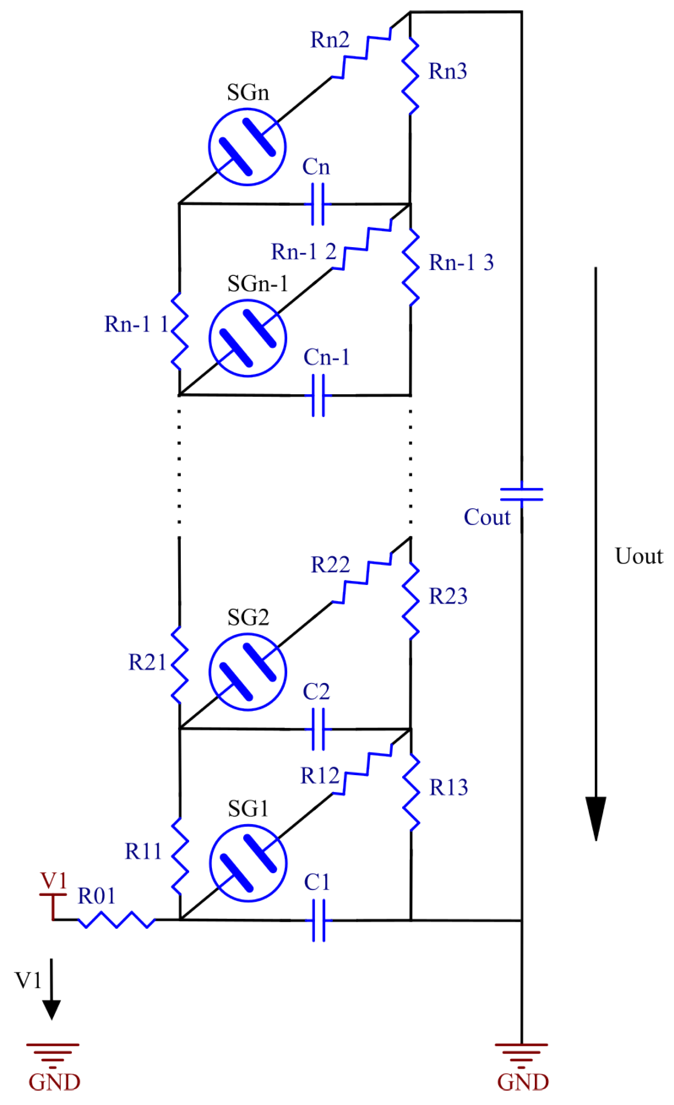
The Marx generator, patented by Erwin Marx in 1923, is a circuit designed to deliver high-voltage pulses by leveraging the principle of charging capacitors in parallel and subsequently discharging them in series to provide energy to a load [
26]. A typical Marx generator configuration is illustrated in
Figure 1. In this setup, each stage contains a capacitor (
) that is charged through resistors (
and
). When the spark gaps (SGs) are triggered, the capacitors discharge through
, resulting in an output voltage that is the cumulative sum of all
n individual stages [
27]. During the early development of the Marx generator, spark gaps were the only available switching devices, achieving rise times on the order of 100 ns, which was considered extremely fast for that era. However, advancements in semiconductor technology have since led to the development of significantly faster switching devices.
Various Marx generators based on solid-state semiconductors have been developed. Using new arrangements with semiconductor switches (MOSFETs, thyristors), their performance (voltage and current outputs, and very fast rise times) can match that of spark gaps and gas switches such as thyratrons [
28].
In the context of this paper, the Marx generator serves as the voltage-boosting step for the pulse generator being developed. By using semiconductor devices—specifically D2PAK thyristors instead of conventional spark gaps—we developed a topology as explained in
Section 2, to enable off-the-shelf components such as SiC MOSFETs and thyristors. This innovative approach enables the delivery of high-voltage and current pulses within sub-nanosecond switching times.
2. Materials and Methods
To achieve ultra-fast thyristor triggering in industrial thyristors, we developed a small thyristor stack generator utilizing thyristors rated at
kV [
29]. These thyristors show a parasitic capacitance of 220 pF while functioning at a bias voltage of
kV, and they possess a static breakdown voltage of 3 kV. As previously stated in
Section 1, the peak voltage required for impact ionization in these thyristors is 6 kV. Therefore, to achieve effective ionization, our triggering generator must provide a voltage of
kV after accounting for the
kV biasing voltage. Therefore, the generator must meet the following operating parameters:
The parasitic capacitance of the thyristor was measured by applying a blocking DC voltage across the anode–cathode range from 200 V to 3 kV, as described in [
23].
2.1. Small-Package Thyristor Marx Generator
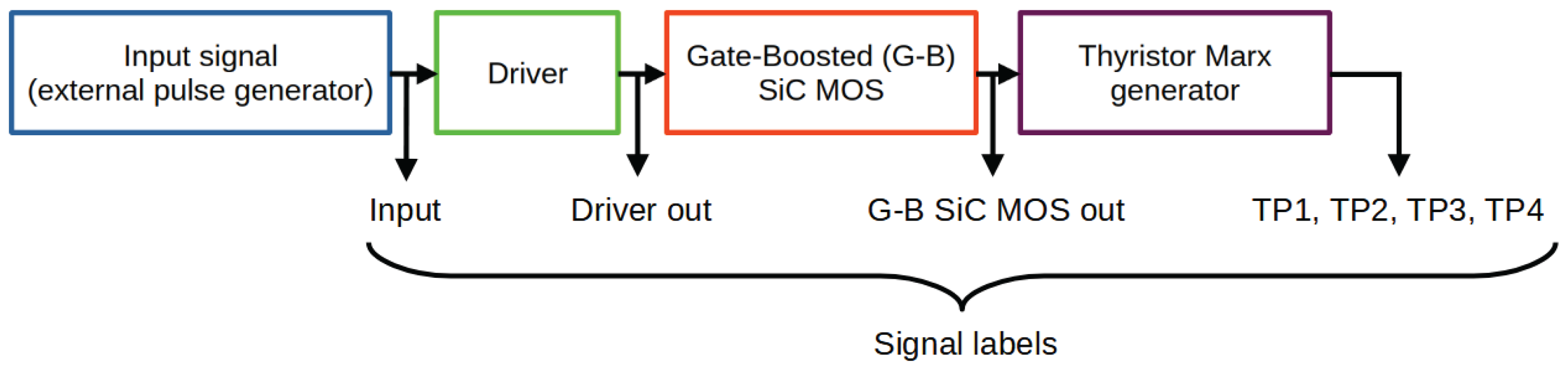
The complete system is illustrated in
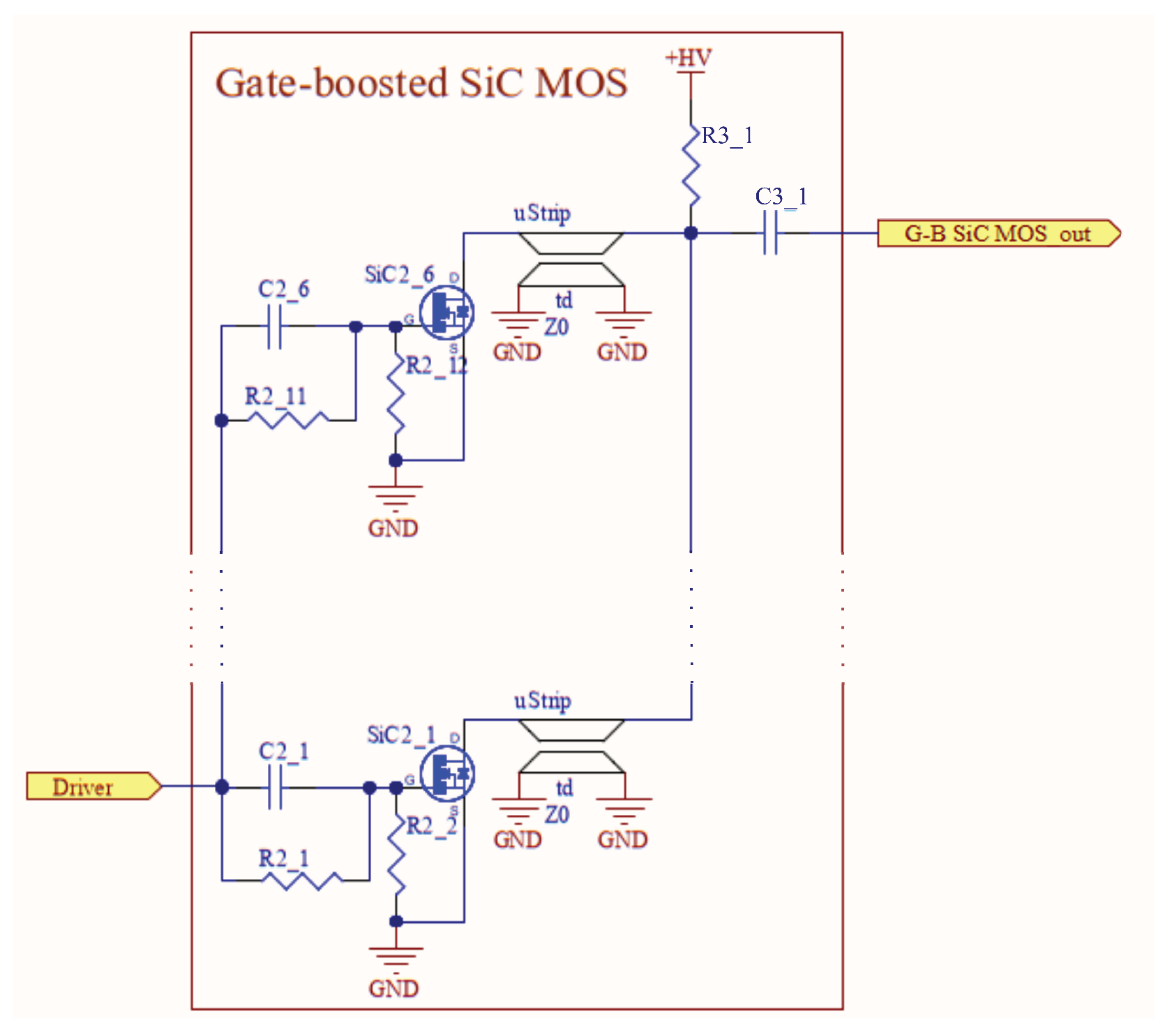
Figure 2, comprising four key stages: the input signal generated by an external pulse generator, which drives the driver stage, followed by the gate-boosted (G-B) SiC MOSFET, and finally the thyristor Marx generator. In the latest iteration of our design, we introduced a configuration of six parallel SiC MOSFET transistors, triggered by the common driver. This arrangement was described in our previous work and is schematized in
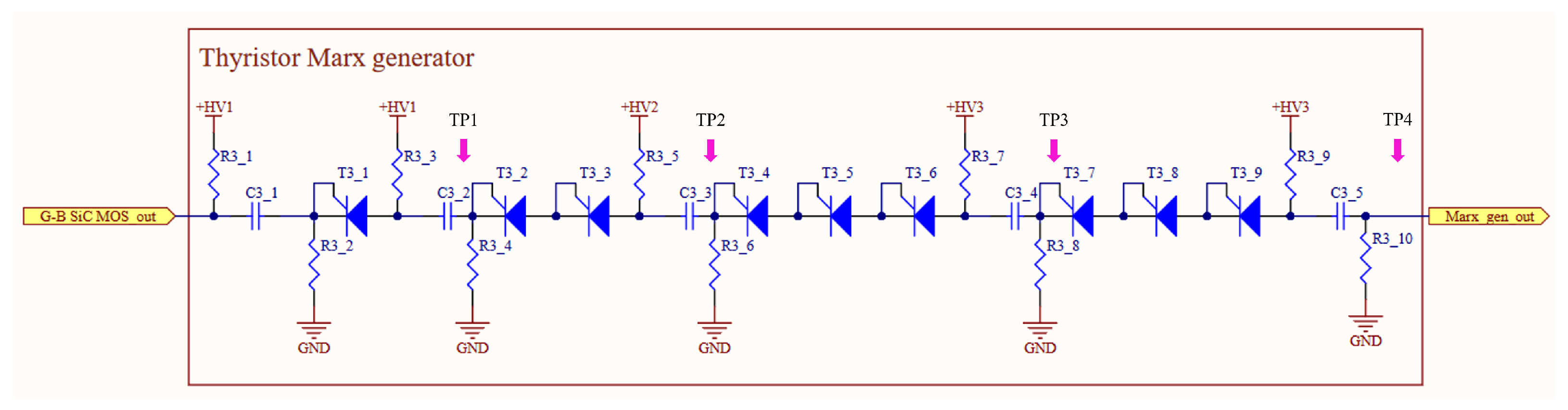
Figure 3. Following this setup, we incorporated a Marx generator composed of small thyristors in D2PAK packages, driven by the pulse output of the six parallel SiC MOSFET. Each stage of the Marx generator effectively adds its storage capacitor voltage (
,
, and
in
Figure 4) while simultaneously sharpening the pulse’s rise time to achieve the power required for a successful impact-ionization triggering.
The number of Marx generator stages can be adapted to meet our target voltage requirements, offering flexibility in design. The datasheet for the D2PAK thyristors [
30] demonstrates great capability in conducting short pulses, with peak currents substantially exceeding their RMS rating by a factor of almost 100 × for nanosecond pulses. The D2PAK thyristors selected for this application are rated for 16 A RMS, with a peak current capacity exceeding 1 kA and a parasitic capacitance of 14 pF. In this iteration of our testing, we opted for a 4-stage Marx generator (
Figure 4).
The first stage of the Marx generator utilizes a single
kV rated thyristor (VS-16TTS12-M3, [
30]). For these thyristors to enter impact-ionization mode, the triggering voltage must far exceed their breakdown thresholds—reaching at least twice their standard values. This triggering signal is derived from the output of six parallel SiC MOSFETs, as shown in
Figure 3, supplemented by the voltage stored in
to enable impact ionization. The increasing number of thyristors in the subsequent stages of the Marx generator is used to manage the rising voltage levels as the pulse propagates through the stages. Each capacitor at the beginning of each stage (
to
adds the corresponding voltage (
) to the pulse. Each additional thyristor helps distribute voltage stress within the stage. Small leakage currents in thyristors increase with the voltage across them, facilitating voltage redistribution. This phenomenon occurs as the leakage current through each thyristor adjusts the voltage stress across its junction, thereby maintaining a stable voltage division [
31]. To enhance this balancing effort, voltage-sharing resistors (
to
connected in parallel with each thyristor have been incorporated to even out voltage differences [
31]. At a maximum charging voltage of 1.3 kV, these resistors ensure a balancing current of about 13
A, significantly exceeding the typical leakage current of 1
A at this voltage. These resistors, however, have been omitted from the schematic in
Figure 4 to improve its clarity and readability.
In our design, we intentionally introduced an impedance mismatch between the six SiC MOSFET stages and the individual Marx stages to generate a positive reflection at the output, facilitating the initial triggering of the thyristor in impact-ionization mode. The primary mismatch occurs in the thyristor before it turns on. At the output of the six SiC MOSFET stages, the circuit can deliver a very high current (370 A) due to its voltage and impedance characteristics, as detailed in our previous publication [
23]. However, the thyristor from the following Marx stage, in its off-state, has a parasitic capacitance of 14 pF, which only draws a small portion of this current (1
14 A). In this state, the thyristor can be approximately considered an open circuit, causing nearly double the voltage to reflect back onto it. As detailed in the same publication, this reflection enhances the voltage pulse at the input of the first stage, contributing to the sharp rise time and increased amplitude available for triggering. This reflection is significantly more pronounced than the impedance mismatch between stages.
To address this, we employed impedance grading, where the impedance of the higher-voltage stage was adjusted to maintain current continuity. After benefiting from this initial reflection, we progressively increased the impedance in subsequent stages (
Table 1). This impedance transition reduces signal reflections at the output and prevents undesired high-voltage spikes, which could otherwise cause excessive stress on the thyristors. The process to find the right impedance value for each stage was performed using LTSpice simulations, which allowed us to adjust said values for each stage. In the LTSpice model, all parameters—except for the impedance values of the transmission lines (Z in the model in
Figure 5)—were fixed based on the schematic. The transmission line impedances were swept to identify the values that minimized signal reflections and improved current continuity. The time delay (Td) values for each stage were determined by the geometry of the setup and remained constant. Once the impedance values were determined, the trace widths were calculated accordingly to match the simulated impedance.
Table 1 presents the calculated impedances and delays of the PCB pads on which the thyristors and capacitors were soldered. The impedance values (Z) were obtained using a FEMM model calculation [
32] with the corresponding dimensions. The resulting values are design approximations, as the calculations do not account for the thyristors and capacitors that bridge the gaps between pads. The method for calculating the delay along an outer stripline on a PCB is based on the method outlined in [
33].
The adjustment of the pad width was made to address variations in the characteristic impedance of the transmission lines. The modulation of impedance was performed to ensure smooth current continuity across the stages. For the initial stage comprising six SiC thyristors, the impedance was calculated as , resulting in a current of at a voltage of kV. In the first Marx stage, the voltage doubles (), necessitating the impedance to also double to maintain the same current. Similarly, the second Marx stage doubles the voltage again (), requiring the previous impedance to double. The third stage adds kV, resulting in a final voltage of kV, which would require an impedance of to maintain the same current. In practical implementation, however, losses such as voltage drops across thyristors and capacitors were observed, resulting in slightly lower voltages than the calculated values. Consequently, the impedance was deliberately set approximately 5% lower than the theoretical value at each stage to account for these losses.
Figure 6 illustrates the physical layout of the Marx generator stages, including the placement of capacitors
to
, which connect the D2PAK thyristors
to
, as well as the charging resistors (
to
). The traces connecting these thyristors are routed with controlled impedance to ensure consistent signal transmission, following the dimensions specified in
Table 1.
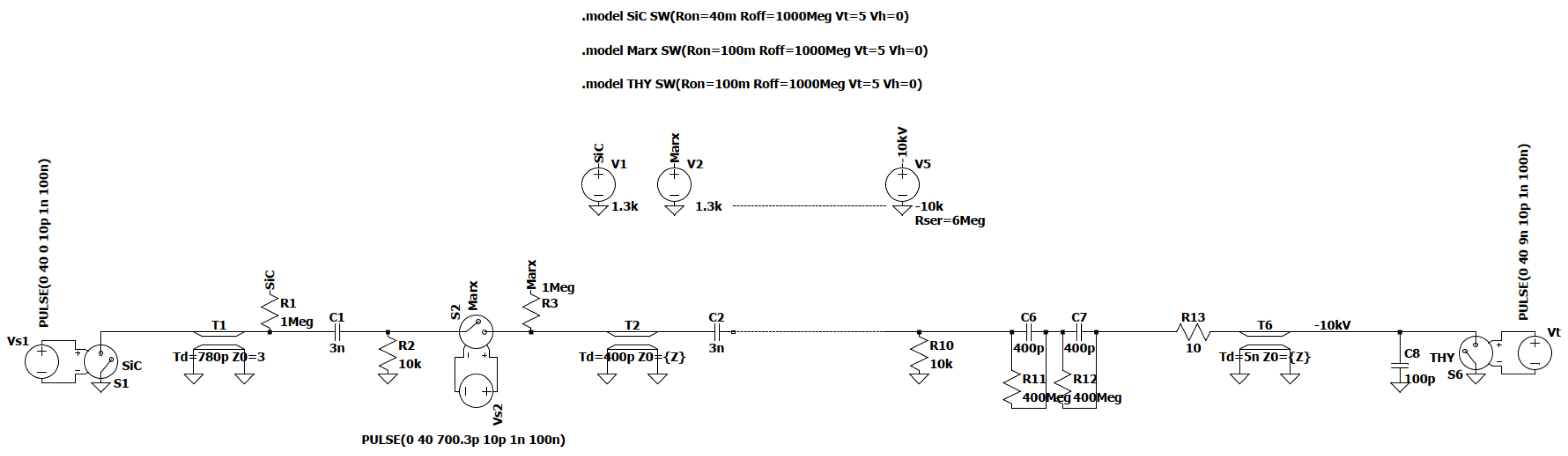
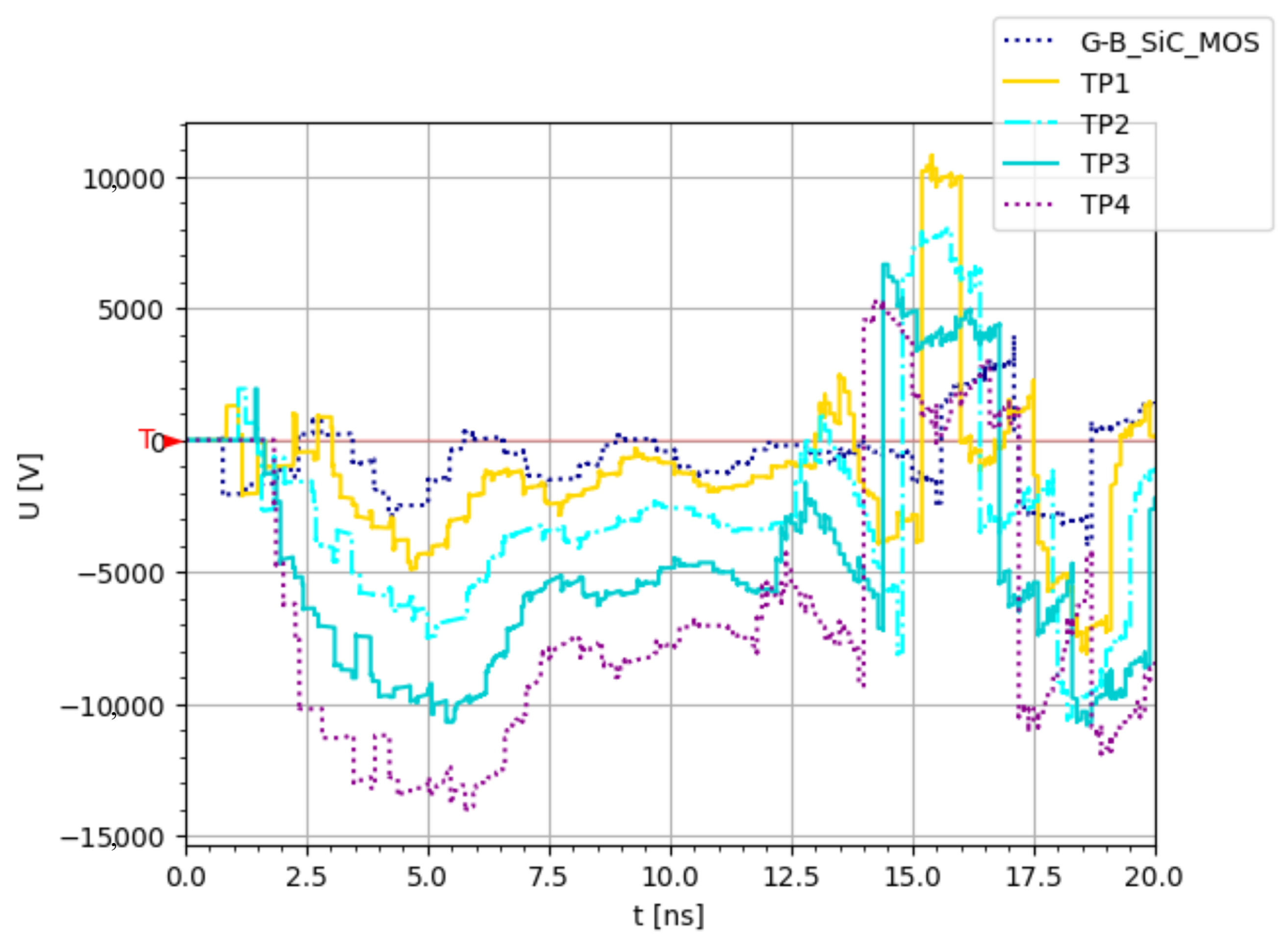
To determine whether an impedance-controlled solution would benefit our design by reducing reflections within the circuit, we conducted an LTSpice simulation comparing a non-controlled configuration with a controlled transmission line impedance configuration (
Figure 5). Our simulation models assume ideal closing switches for both SiC MOSFETs and thyristors, providing an approximate representation of the system rather than an exact prediction of the real setup. The primary objective is to gain an initial understanding of the circuit behavior, offering preliminary insights to guide the design process. No readily available simulation model accurately captures the performance of SiC MOSFETs in gate-boosted mode or thyristors in impact-ionization mode. Since precise modeling of their real behavior was not the priority at this stage, we opted to represent all switching components as ideal closing switches to focus on overall circuit operation. Stages 2–4 are represented by a dotted line, along with their corresponding biasing voltage sources, for better visualization. The simulation was conducted under conditions representative of the actual operational environment of the circuit, aiming to indicate the effects of signal reflections and impedance mismatches on ideal switches. The transmission lines were modeled with varying impedances to compare the effects of controlled versus non-controlled impedance configurations following the values in
Table 1, which also includes the corresponding calculated delay for each stage.
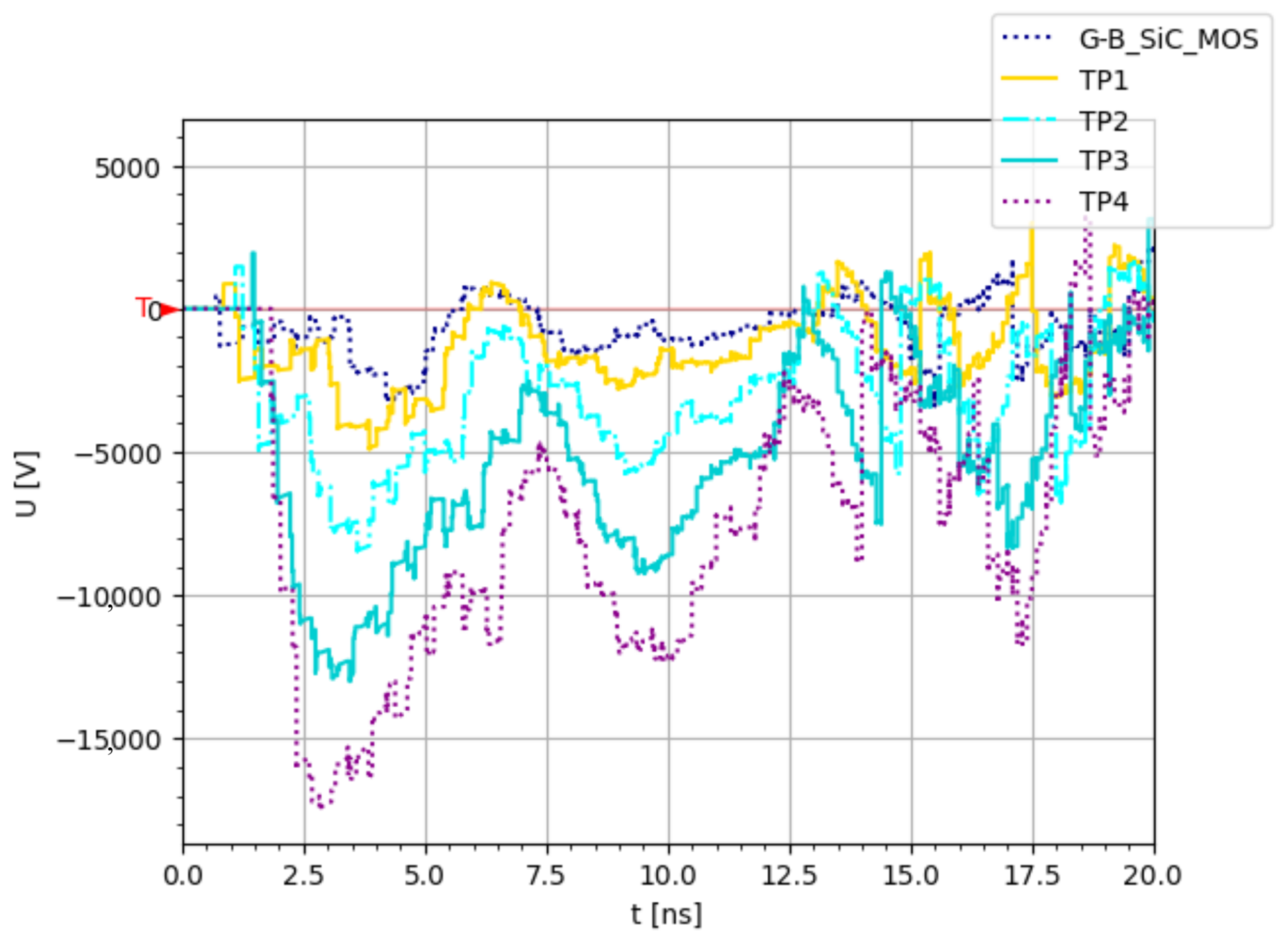
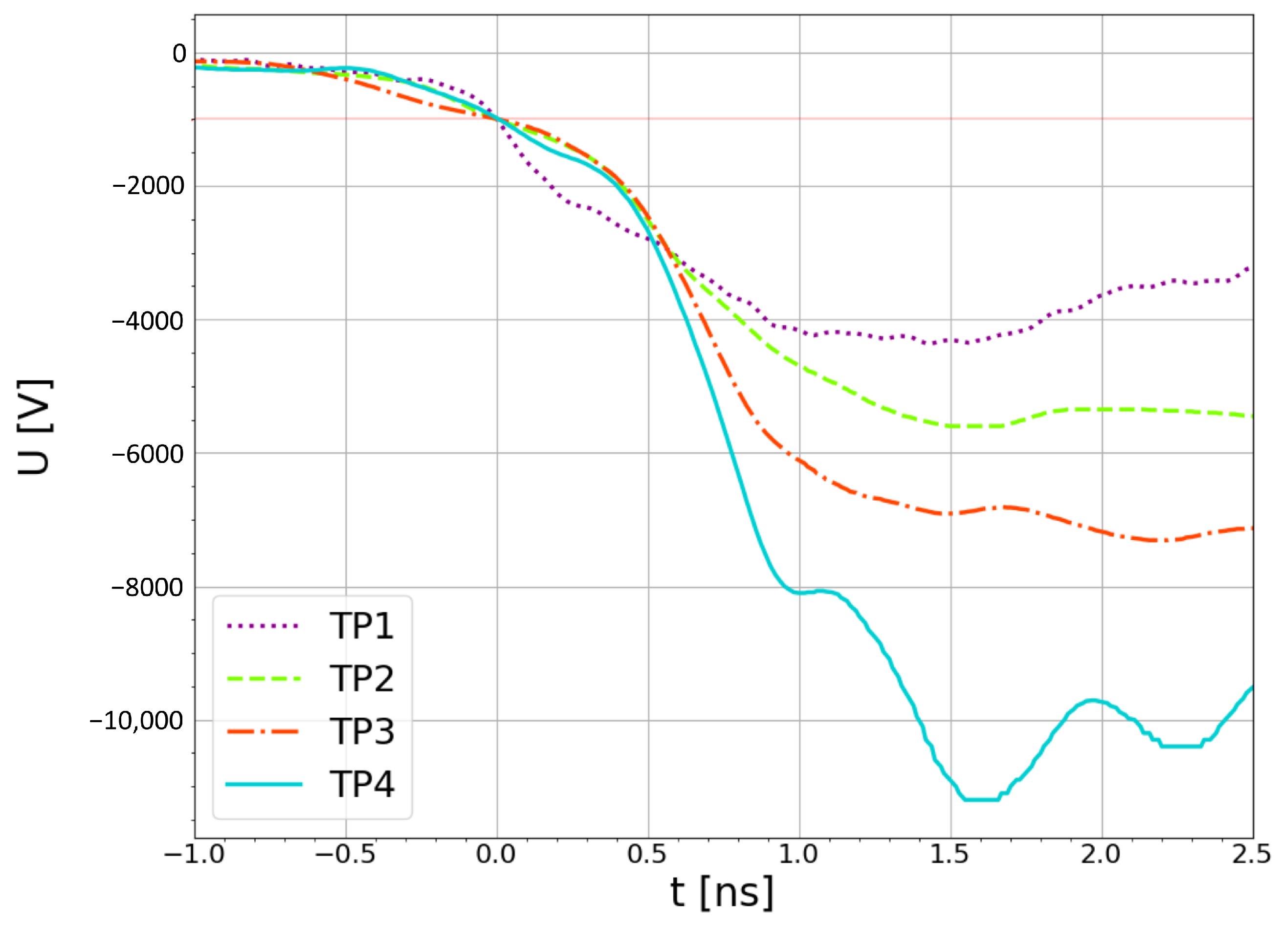
To assess the impact of controlling the impedance of the transmission lines on the reflections, we positioned our test point at the first switch, S1, which represents the six parallel SiC MOSFETs. We compared the current passing through this switch in both the impedance-controlled model and the non-controlled model, where each stage was set to a uniform 20 impedance. This value is based on the approximate pad impedance of a D2PAK casing, which is the minimal width suitable for the D2PAK thyristors in our design.
The simulation illustrates the voltage distribution across all stages in
Figure 7 and
Figure 8, including the SiC MOSFETs (
) and thyristors (
to
), providing insight into the system’s behavior. While the simulation does not perfectly match reality, it effectively demonstrates the progressive voltage amplification and associated delay, as well as the reflections and their attenuation over time. It can be observed that the reflections in the controlled impedance case (
Figure 8) demonstrate less amplitude than in the fixed 20
case (
Figure 7). Additionally, the results in
Figure 9 show that the 20
configuration causes higher peaks from the signal reflections, which can reach up to 2 kA. In contrast, the controlled impedance approach reduces the amplitude of the reflections, keeping them within the ±1 kA range.
2.2. Capacitive Probe
During the testing of the pulse generator, we encountered significant challenges with our measuring equipment, particularly with the standard high-voltage (HV) and high-frequency (HF) attenuators that we utilized. These devices began to experience breakdowns when subject to output voltages surpassing 6 kV, as explained in [
34].
To address this issue cost-effectively, we transitioned to an alternative method—namely, capacitive probes—to measure the output voltages. This adjustment provided a more robust measurement configuration. This adjustment provided a more robust measurement configuration by mitigating escalating voltage levels and ensuring the oscilloscope and attenuator were protected from excessive voltage exposure, as capacitive probes can withstand higher thresholds.
Capacitive probes offer the advantage of non-contact voltage measurements, thereby preserving the integrity of the oscilloscope and attenuator by reducing the voltage that reaches these sensitive instruments [
35]. Their application is well-established within the pulsed power community for testing high-voltage, fast pulses [
36], and they have been successfully developed in laboratories utilizing printed circuit board (PCB) techniques [
37].
Integrating capacitive sensor plates into the existing PCB design eliminates the need for additional components, leveraging the intrinsic capacitance between the probe and the test point. This non-contact approach significantly reduces the risk of arcing and damage to delicate components, thereby ensuring a safer measurement environment. The 2 mm capacitive probe is positioned beneath the much larger target signal plane, allowing for effective voltage measurement without direct electrical contact.
We recognized that the accuracy of our capacitive probe measurements could be influenced by both the voltage amplitude and the frequency of the signal due to the frequency-dependent limitations of FR4, as documented in recent studies ([
38,
39,
40]). To mitigate these concerns, we maintained consistent geometrical dimensions for the capacitive probe and its associated high-voltage island, following the recommendations from the aforementioned literature ([
38,
39,
40]) to ensure reliable calibration.
In our setup, the capacitive probe functions as a first-order high-pass filter.
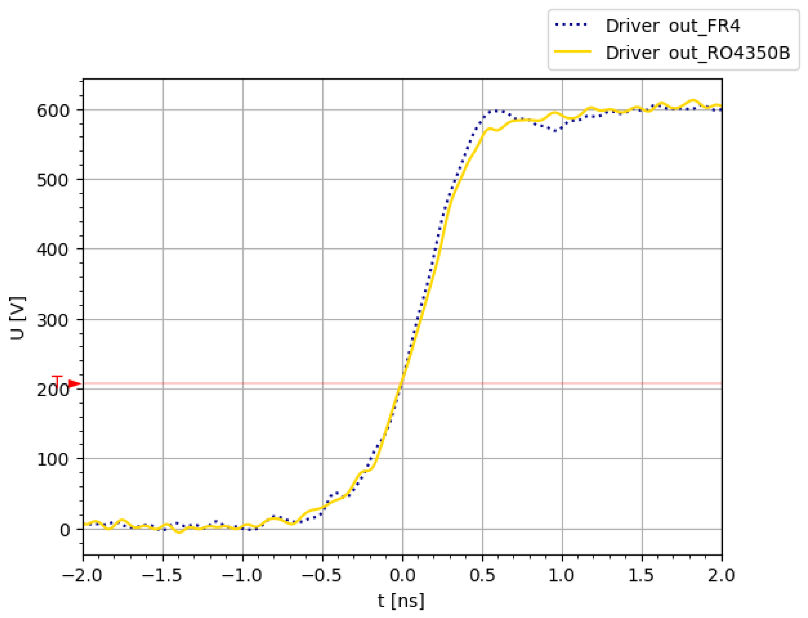
The choice of FR4 as the PCB material could potentially limit high-frequency measurements as the choice of material affects the upper-frequency limit due to dielectric losses. We conducted comparative measurements of the driver output using both our current FR4 PCB and a high-frequency PCB material (RO4350B) [
41] (
Figure 10). The results indicated no significant improvement in rise time (FR4: 680 ps; RO4350B: 768 ps), leading us to continue using FR4 for further measurements as it meets our requirements without imposing limitations on the bandwidth of the capacitive probe while having the added advantage of being more economically priced.
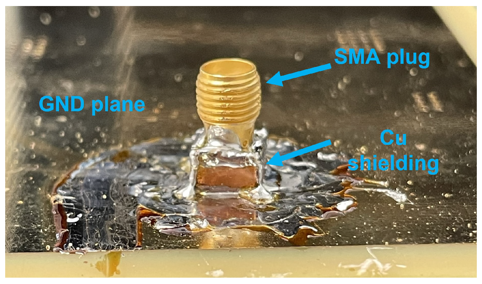
The final PCB setup, illustrated in
Figure 11, features a 2 mm diameter pad connected to an SMA plug for the measurement cable connection, with copper shielding included to enhance signal accuracy.
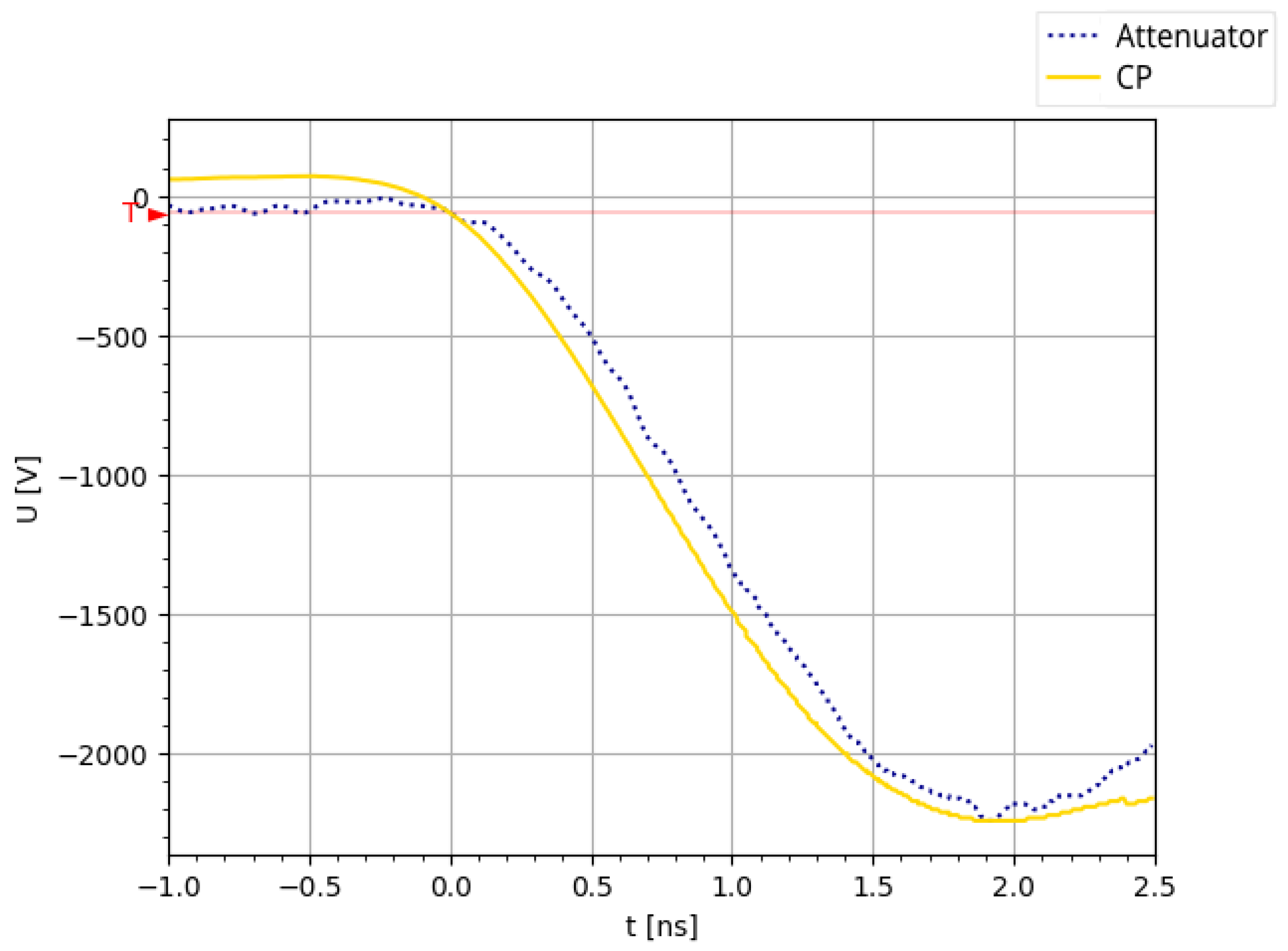
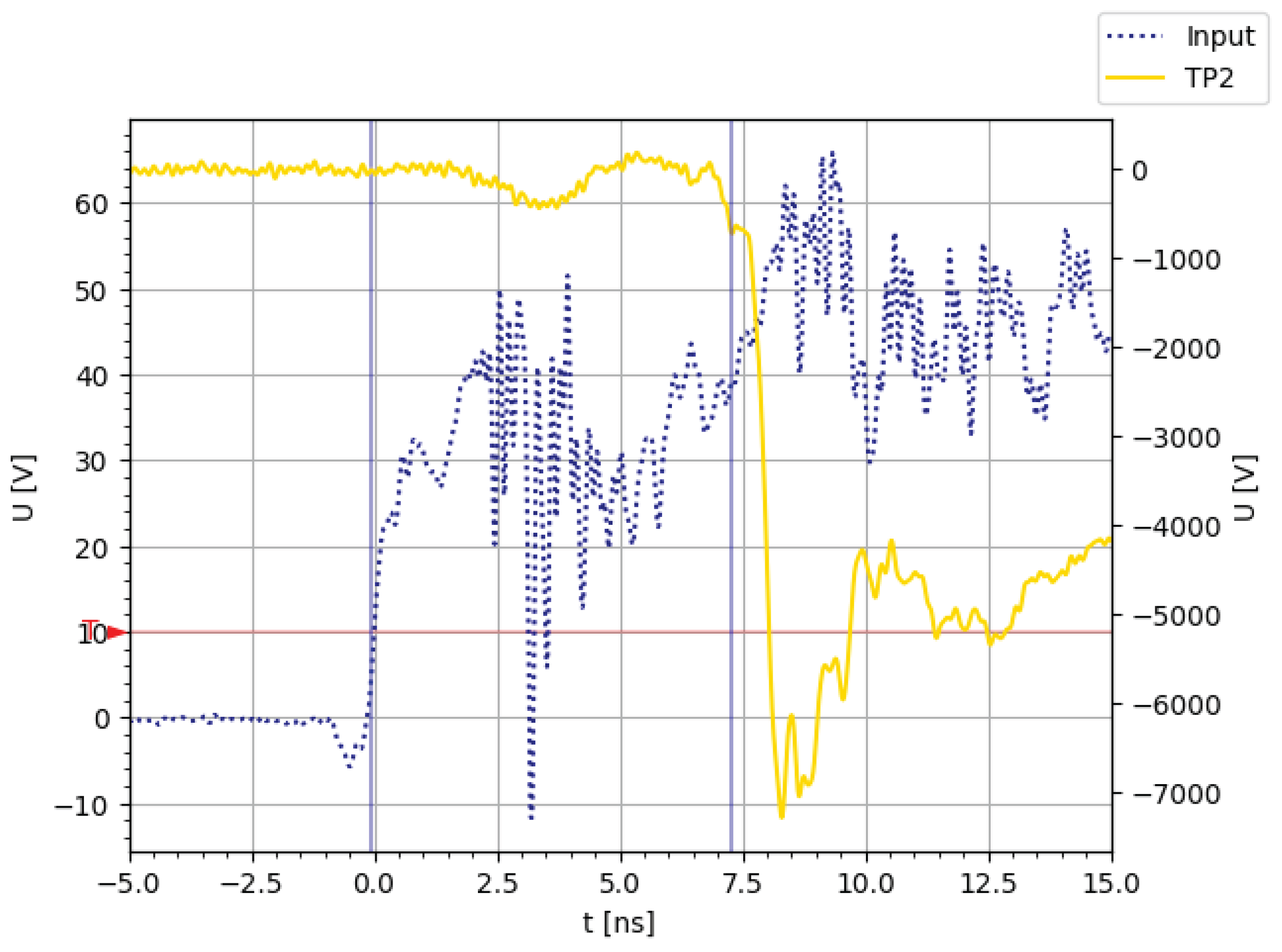
To evaluate the accuracy and reliability of the capacitive probe, we conducted a series of tests comparing the probe’s measurements with those obtained using a standard coaxial cable (RG58) connected to a 50 attenuator. Due to the attenuator’s voltage rating limitations, measurements were performed such that the resulting output signals reached a maximum of kV. Both measurement methods were employed simultaneously to assess performance. The same signal was measured simultaneously using both the capacitive probe and the coaxial cable setup.
Figure 12 presents a comparison of the two measurement methods at the input (G-B SiC MOSFET out,
Figure 4), with the attenuator measurement represented by the blue line (
), and the capacitive probe measurement represented by the yellow line (
). The biasing voltage for the SiC MOSFETs is set at
kV during operation. A lower voltage would not ensure sufficiently fast switching, while a higher voltage risks damaging the MOSFETs. A linearity test is pending to verify the accuracy of the system within the lower voltage range permissible by the reference measurement system, ensuring that performance scales appropriately across the intended operational voltage spectrum.
Future work should include a comprehensive linearity check, extending to an anticipated voltage of 10 kV to validate both the system’s voltage linearity and the associated electric field stresses on components. This assessment will confirm the safe operational limits of the FR4 dielectric material’s electric field strength, as well as examine its dielectric strength and lifetime under repetitive 10 kV pulsing, ensuring measurement accuracy and durability of the system over prolonged use.
In summary, our exploration and implementation of capacitive probes for high-voltage measurements, embedded within the PCB, have enabled us to achieve sub-nanosecond measurements while safeguarding our measuring equipment.
4. Summary
This research focuses on developing an innovative methodology for triggering industrial thyristors in high-voltage applications, particularly within particle accelerators. By employing boosted gate triggering, we substantially improve the switching dynamics of SiC MOSFET devices, enhancing both dU/dt and dI/dt performance. The improved output pulse from these SiC MOSFETs is then fed into a small-package thyristor Marx generator, which sharpens the falling edge and amplifies the pulse amplitude. This approach accelerates operation while enhancing efficiency, outperforming conventional triggering techniques.
This work explores recent developments in pulse sharpening and amplification, designed to achieve the required voltage, current, and dU/dt for triggering a stack of thyristors in impact-ionization mode. By pushing the boundaries of the operational capabilities of COTS components, we increased both voltage and current outputs while maintaining sub-nanosecond switching times. The resulting pulse generator operates near the limits of switching performance, reaching a turn-on slew rate of over 1 kV/ns. However, the output voltage at the SiC MOSFET level does not yet reach the triggering voltage required for kV rated thyristors. To address this limitation, a D2PAK thyristor-based Marx generator has been incorporated.
The proposed solution, while it involves various challenges, offers significant advantages. Utilizing compact topologies and commercially available components has led to a smaller, reproducible design with the potential for cost savings. Additionally, the technology’s rapid response to beam dump requests suggests it could serve as an alternative to traditional systems in particle accelerators, potentially offering enhanced performance. However, further validation in real-world operational conditions is required to confirm its feasibility for full implementation. Our method minimizes the delay between the trigger request and the output signal by allowing direct signal propagation through the stages. In comparison, the opening switch approach necessitates a preparation time exceeding 500 nanoseconds. Alongside these significant findings, we have introduced an innovative and simple means of measuring high-voltage (HV) pulses seamlessly integrated within a PCB, all while keeping costs to a minimum.
Looking ahead, further research will involve testing this pulse generator as the trigger for a stack of thyristors to achieve higher output voltages and currents. We developed technology capable of responding in nanoseconds, such as for beam dump requests, significantly reducing reaction times by two orders of magnitude compared to current technologies. Demonstrating that this triggering method is both reliable and economical for accelerator systems could pave the way for its adoption in place of prevailing thyratron-based systems.


 ,
, 

