1. Introduction
Time synchronization technology plays a crucial role in multiple key areas, particularly in China’s spallation neutron source, where neutron spectrometer experiments generate neutrons by bombarding a target material with proton beams and collecting information on each neutron pulse corresponding to the proton pulse. In this process, the beam monitoring nodes need to maintain absolute clock synchronization to ensure the accuracy of the data and the reliability of the experimental results. The demand for high-precision clock synchronization is not only applicable to neutron spectrometer experiments but also plays an important role in various critical fields such as radar, radio frequency systems [
1], synchrotron accelerators, and smart grids [
2]. Therefore, in-depth research and optimization of clock synchronization technology have broad application prospects. As the demand for time precision in these fields continues to increase, the need for switching devices capable of supporting high-precision time synchronization has also surged. Switches, as core devices for data transmission and synchronization signal distribution, play a vital role in building reliable low-latency network architectures. Consequently, switches equipped with advanced time synchronization technology have become essential infrastructure to meet the demands of modern applications.
Network time synchronization technologies such as NTP [
3,
4,
5], PTP [
6,
7], and dedicated fiber optic time synchronization have been widely used in various scenarios. However, each of these technologies has certain limitations and cannot meet the stringent accuracy requirements for time synchronization in demanding fields. Especially in time-sensitive fields that require ultra-high timing and synchronization performance, such as national time and frequency laboratories and particle accelerators, these traditional technologies often fall short. In order to overcome these challenges, White Rabbit (WR) technology [
8] has emerged. WR technology is a sub-nanosecond clock synchronization technology based on standard Ethernet [
9], jointly proposed by the European Organization for Nuclear Research (CERN) and the GSI Helmholtz Centre for Heavy Ion Research in 2008. With its outstanding performance, it not only overcomes the limitations of traditional time synchronization technologies but also offers numerous significant advantages.
WR technology supports frequency distribution and time synchronization over multiple nodes and long distances [
10,
11]. It is fully compatible with standard gigabit Ethernet protocols and features low cost, high bandwidth, high reliability, and flexible topology, among other characteristics. This gives WR technology tremendous application potential in time-sensitive fields, as it not only meets the stringent requirements for time synchronization accuracy but also promotes the further development of time synchronization technologies. It opens up new possibilities for the diversification of future time synchronization applications. As an innovative technology in the field of time synchronization, WR technology is leading the way toward a new era of greater precision, efficiency, and reliability in this domain.
WR switches (WRS) are the core components of WR networks. They are built upon standard switches with added WR functionality and provide features such as QoS support, link redundancy, and fast switching to meet the high real-time requirements of clock and control systems. Additionally, they can distribute time–frequency signals to multiple connected WR devices, enabling the construction of time synchronization networks with nearly ten thousand nodes. After extensive research, the following issues have been identified with WRS: (1) they use a discrete component architecture, specifically a combination of MCU and FPGA, which connects the two through an external EBI bus, making the communication process somewhat complex; (2) creating a Linux system on the MCU side is not sufficiently convenient; and (3) the expandability is limited, as the current hardware is inadequate to support the addition of new functionalities.
To address these issues, a time synchronization switch with WR functionality has been designed based on the Zynq platform. This switch not only achieves independent control but also reduces the physical size of the design. The PS and PL communicate via an internal AXI bus, which can minimize external environmental interference, making time synchronization more precise and stable. Using the Xilinx built-in development tool simplifies the development process and improves development efficiency. The hardware–software co-design capabilities of Zynq allow developers to flexibly adjust task allocation and resource utilization based on application requirements [
12].
The remainder of this paper is organized as follows.
Section 2 introduces the principles of WR technology.
Section 3 presents the hardware implementation plan for the time synchronization switch.
Section 4 discusses the implementation of the time synchronization module.
Section 5 validates the time synchronization functionality.
Section 6 provides a conclusion.
2. WR Technology
WR combines three mature technologies: synchronous Ethernet (SyncE) [
2], Precision Time Protocol (PTP), and Digital Dual Mixer Time Difference (DDMTD) [
13,
14]. SyncE ensures that all clocks within the network operate at a common frequency [
15]. PTP is responsible for achieving coarse synchronization of the clock phase information, while DDMTD measures finer clock phase differences to ultimately achieve clock synchronization across all network nodes [
16], allowing the system’s synchronization accuracy to reach sub-nanosecond levels.
2.1. Synchronous Ethernet (SyncE)
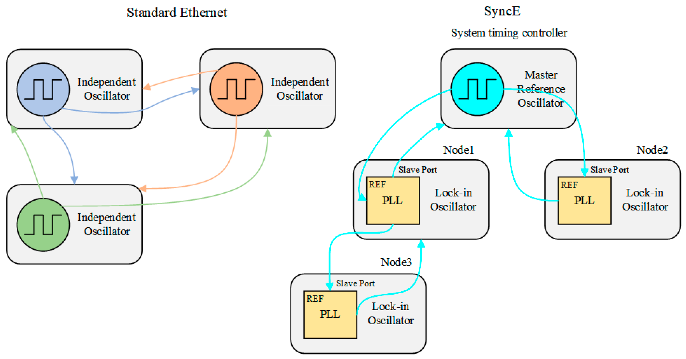
SyncE is a technology used to achieve frequency synchronization between devices [
17]. Its main working principle is to extract clock signals from the received serial data stream using Ethernet physical layer chips. This process typically occurs within the physical layer (PHY) chip, for example, using a digital phase-locked loop (PLL). The extracted clock signal can be output via the BITS interface or can be further transmitted to downstream devices through Ethernet data.
SyncE employs a hierarchical synchronization network, where the top-level node is referred to as the System Clock Master (STM). It is synchronized with a master reference clock (such as a GPS receiver or atomic clock) and serves as the frequency reference for the entire network. Each node uses the synchronized clock signal received from upstream as the reference for its own clock and subsequently passes it on to downstream nodes, ensuring frequency consistency throughout the entire network [
18], as illustrated in
Figure 1.
The advantage of SyncE lies in its relatively simple implementation, as it is not affected by higher-layer protocols. Therefore, it is not impacted by factors such as data network congestion, packet loss, and delay. This allows SyncE to provide clock accuracy similar to that of SDH (Synchronous Digital Hierarchy)/SONET (Synchronous Optical Network) networks, making it suitable for scenarios that do not require high precision in time synchronization. However, it is important to note that SyncE only supports frequency synchronization and does not support time synchronization. Moreover, because SyncE relies on physical layer signal transmission, it tends to have relatively low flexibility in terms of network topology.
2.2. Precision Clock Protocol (PTP)
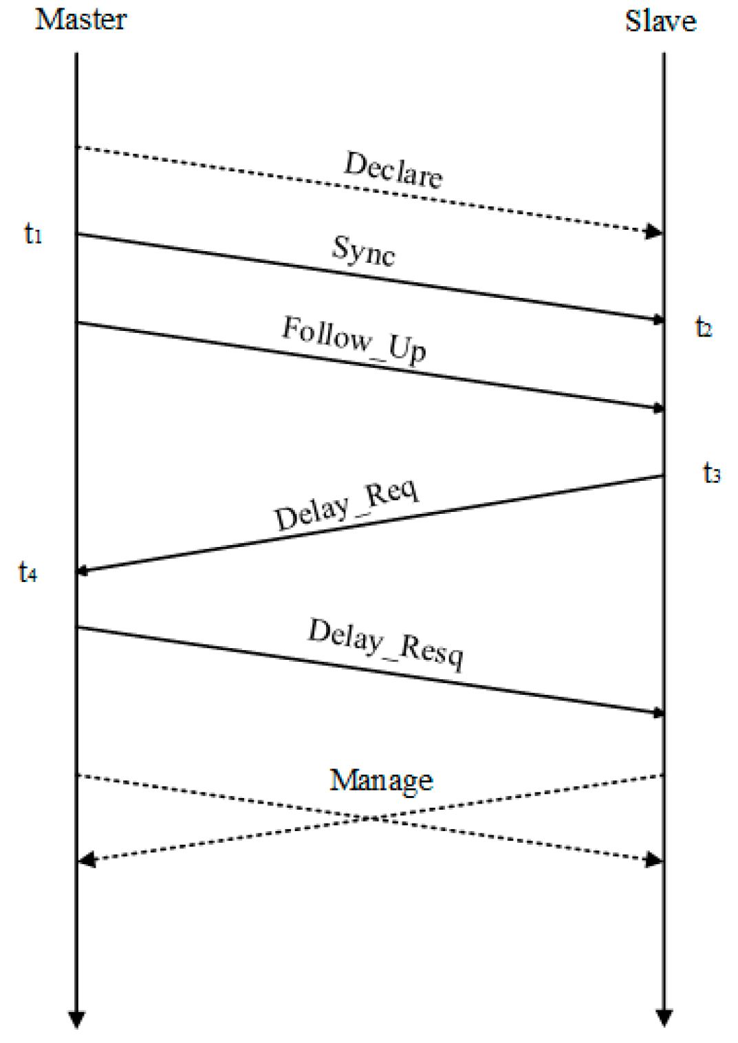
PTP is a high-precision time synchronization protocol based on the IEEE 1588 standard, designed to provide solutions for applications that require synchronization at the sub-microsecond level. Compared to the traditional Network Time Protocol (NTP), the main advantage of PTP lies in its ability to achieve higher precision in time synchronization. PTP achieves nanosecond-level time precision in wired networks by generating timestamps at the hardware level, thereby eliminating delays and inaccuracies introduced by the operating system and software processing [
19]. This high-precision synchronization capability makes PTP particularly suitable for fields with extremely strict time requirements, such as industrial automation, power systems, and financial market trading. In addition, PTP employs a master–slave structure for clock synchronization in the network [
20,
21]. The master clock is responsible for transmitting time information to the slave clocks by continuously exchanging message packets that contain timestamps of the sent and received times. The slave clocks then calculate the time deviation based on the synchronization algorithm and perform self-adjustments to achieve synchronization with the master clock. The synchronization process of PTP is illustrated in
Figure 2.
(1) At time , the master clock sends a Sync message, placing the timestamp information in the Follow_Up message.
(2) At time , the slave clock receives the message and obtains the timestamp from time .
(3) At time , the slave clock sends a Delay_Req message.
(4) At time , the master clock receives the message and then sends a Delay_Resp message. The slave clock records the four timestamps.
According to the PTP, the one-way transmission delay (
) and the offset between the master and slave clocks (
) can be calculated, assuming that the round-trip delay of the messages between the master and slave clocks is symmetrical, as shown in Formulas (1) [
9] and (2) [
22].
2.3. Digital Dual Mixer Time Difference (DDMTD)
The DDMTD features good linearity and a wide dynamic range, and it has no dead zone. Compared to traditional DMTD structures, it is simpler and more cost-effective. The DDMTD can convert phase deviation from high frequency to low frequency, making it very suitable for measuring two closely spaced signals. This can greatly eliminate several common types of phase noise.
Figure 3 illustrates the internal structure of the DDMTD. It samples two square wave clock signals,
and
, using two D flip-flops in order to measure the phase difference between them. The offset frequency is generated from one of the measured signals through a phase-locked loop (PLL), as shown in Equation (3) [
23].
The principle of the DDMTD can be described by making a visual comparison with a conventional vernier caliper. The vernier caliper has two scales: the millimeter scale and the vernier scale. The vernier scale is used to enhance the measurement precision of the millimeter scale by providing a decimal fraction. A typical vernier caliper’s vernier scale is divided into ten intervals, with each interval measuring 4.9 mm in length. When any interval on the vernier scale aligns with any interval on the millimeter scale, the measurement result will include a decimal fraction. The millimeter scale corresponds to the input clock, while the vernier scale corresponds to the offset clock. Whenever the intervals on the two scales align, the output signal will change.
Figure 4 shows an example of the two measured clocks and the output signal they generate.
In this design, N is set to 14. The sampling operation performed by the flip-flops is similar to analog mixing and low-pass filtering. Therefore, the frequencies of the output clock signals clk
Aout and clk
Bout are proportional to the frequencies of the input clock signals. The phase between the input signals is equal to the phase between the output signals; thus, the difference between the edges of the input and output clock signals is proportional, as described in Equation (4).
When the input clock is 62.5 MHz, the output DDMTD clock frequency is 62.496185 MHz after passing through a PLL. The down-converted clock frequency produced by the DDMTD is 3.814 kHz. Since each rising edge of these clock signals is timestamped, the phase information is provided to the PLL at the DDMTD frequency. This is indeed the sample rate of the SoftPLL, and thus its Nyquist frequency is 1.9 kHz. According to the current parameters, the time resolution can be calculated as 0.977 picoseconds using Equation (5).
3. System Hardware Design
Xilinx’s Zynq products are mainly categorized into the following types based on different application scenarios and performance requirements:
(1) Zynq-7000 SoC Series
The Zynq-7000 series integrates ARM processors with programmable logic in FPGA, supporting the co-design of hardware and software. This series offers a variety of models with different logic resources, storage capacities, and interface counts to meet diverse application needs.
(2) Zynq UltraScale+ MPSoC Series
The Zynq UltraScale+ MPSoC series provides more powerful performance and richer functionality, equipped with more processor cores, larger storage capacity, and higher communication bandwidth. These devices support various security features, making them suitable for applications that require high levels of security.
(3) Zynq UltraScale+ RFSoC Series
The Zynq UltraScale+ RFSoC series has a similar architecture to the MPSoC but is optimized for radio frequency (RF) signal processing. It integrates a large number of RF-related modules and functionalities, such as ADCs and DACs, enabling direct acquisition and processing of RF signals, which significantly simplifies the design complexity of RF systems.
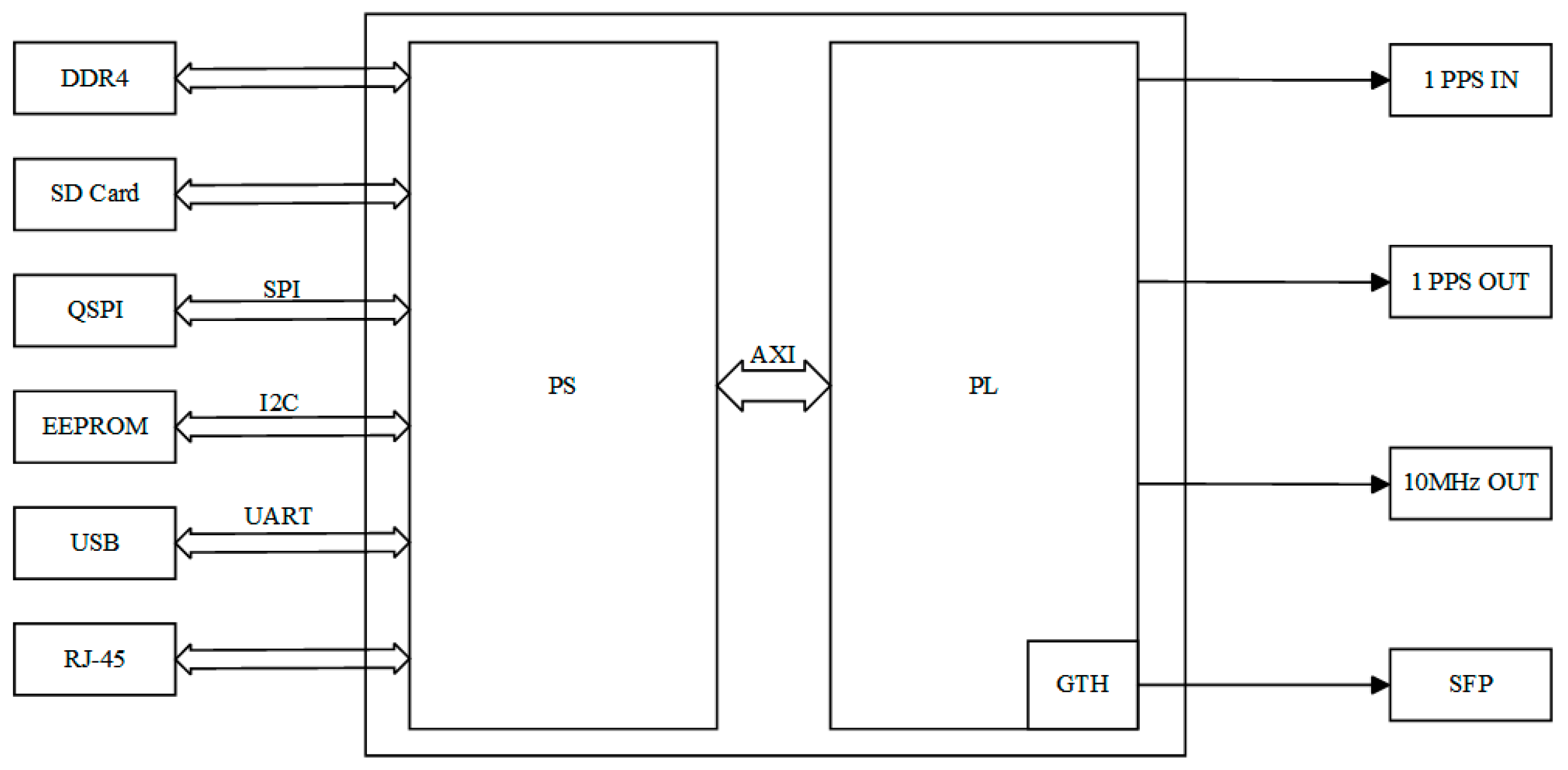
The goal of this design is to achieve time synchronization while selecting faster transmission interfaces and rich external interfaces for future improvements. Therefore, we have decided to use a chip from the Zynq UltraScale+ MPSoC series. Additionally, the hardware logic required for time synchronization needs at least four MMCMs and four PLLs to support the overall performance of the system. Considering resource utilization and manufacturing costs, the Zynq UltraScale+ XCZU9EG-1FFVC1156 chip was ultimately chosen.
The specific design block diagram is shown in
Figure 5. The PS side mainly includes hardware such as DDR4, SD card, QSPI Flash, and EEPROM, while the PL side mainly includes hardware such as SFP, UART, and FMC. The PS side is responsible for running the Linux operating system and related software, while the PL side is responsible for implementing the time synchronization function.
3.1. Power Circuit
The power supply voltage for the switch is specified as 12 V. In the power supply design, it is necessary to convert the 12 V power supply to 0.85 V for the Zynq core voltage using the LTM4630A chip, in order to meet the power consumption requirements during data processing. Additionally, an LTM4644 chip is used to generate other voltages required for the various banks of the Zynq and the clock synchronization module.
3.2. Clock Circuit
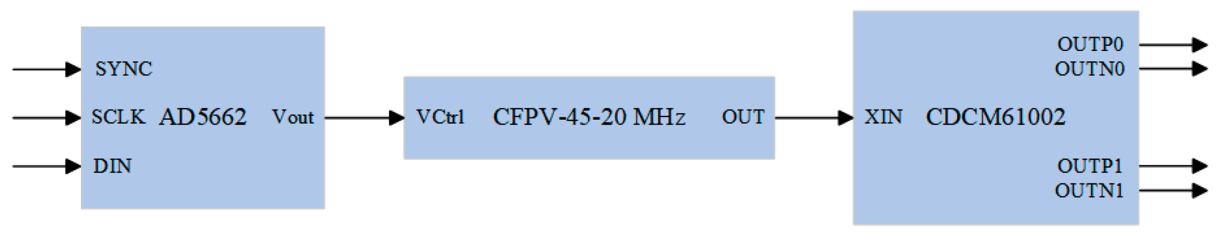
The WR technology requires an external adjustable hardware clock to support the digital dual-mixing time reference technology. Therefore, a 25 MHz Voltage Controlled Crystal Oscillator (VCXO) is selected to drive the low-jitter clock generator chip CDCM61004RHBT, which provides the required 62.5 MHz clock and serves as the reference clock for the DDMTD. The specific scheme is shown in
Figure 6.
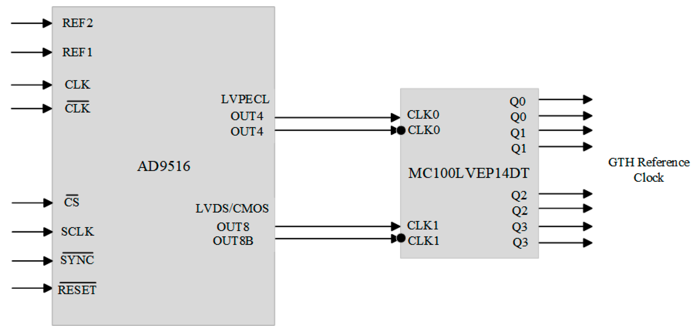
The AD9516 can select either one differential or two single-ended reference inputs. In this design, the two single-ended reference input configurations are chosen. By configuring the SPI module, the chip outputs multiple 62.5 MHz clocks, with one of the outputs serving as the reference clock for the PL. Two of the outputs are extended to five outputs, all serving as reference clocks for the GTH. The specific scheme is shown in
Figure 7.
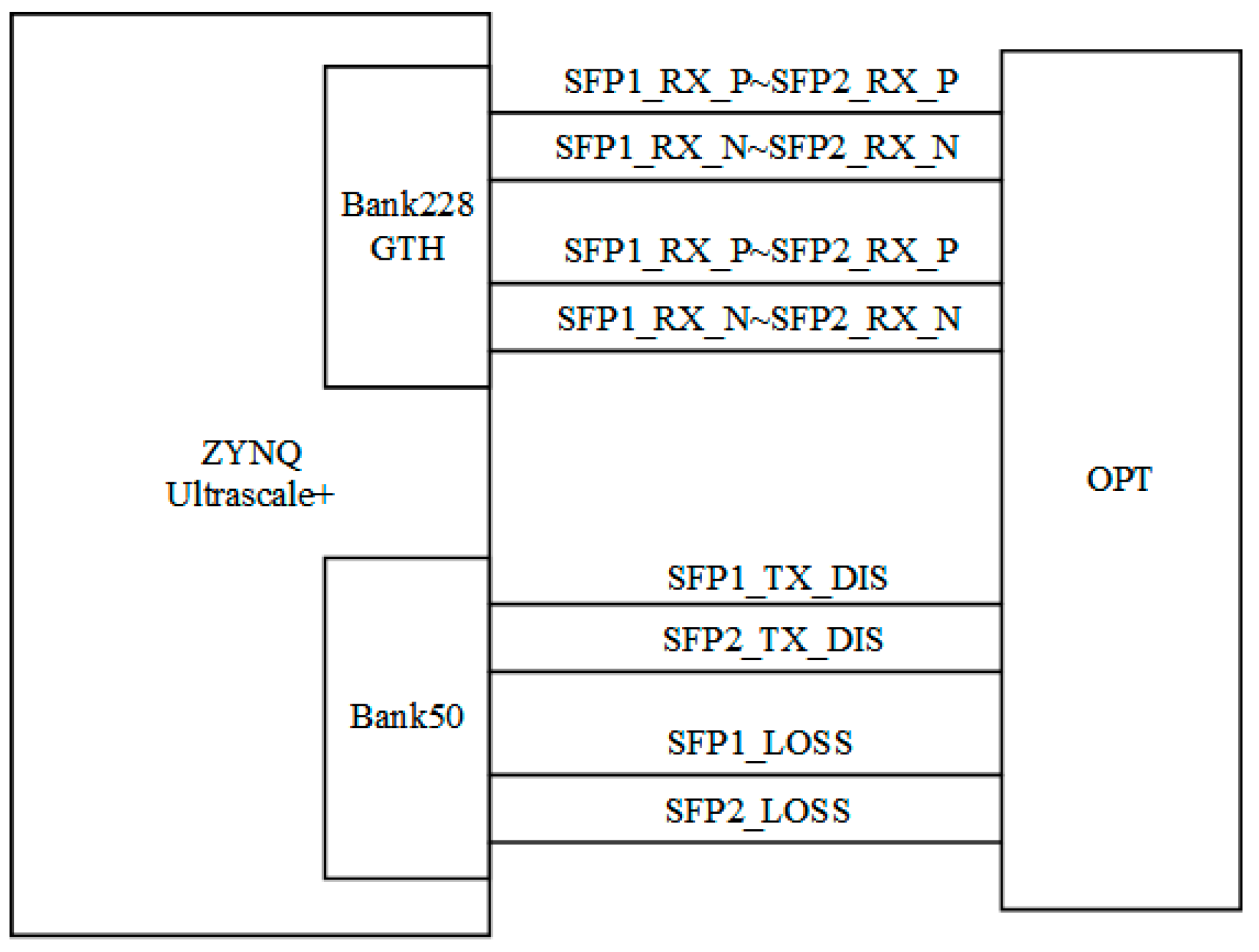
3.3. SFP Interface Circuit
In order to enhance transmission speed while ensuring long-distance data transmission, optical fiber is selected for data transfer. The SFP interface module is connected to the GTH transceiver of the Zynq, and the block diagram of the SFP interface design is shown in
Figure 8, with a data transmission rate of up to 12.5 Gb/s.
For the selection of SFP types, they can be classified based on transmission distance, mainly into three categories—short-range, medium-range, and long-range—in order to meet diverse clock synchronization requirements. The optical module chosen for this design has a transmission wavelength of 1310 nm and a receiving wavelength of 1490 nm. The GTH interface supports multiple network transmission protocols. If it is necessary to change the physical layer network interface of the GTH, this can be achieved by modifying the GTH IP core or its source code, thereby allowing for the extraction of timestamps.
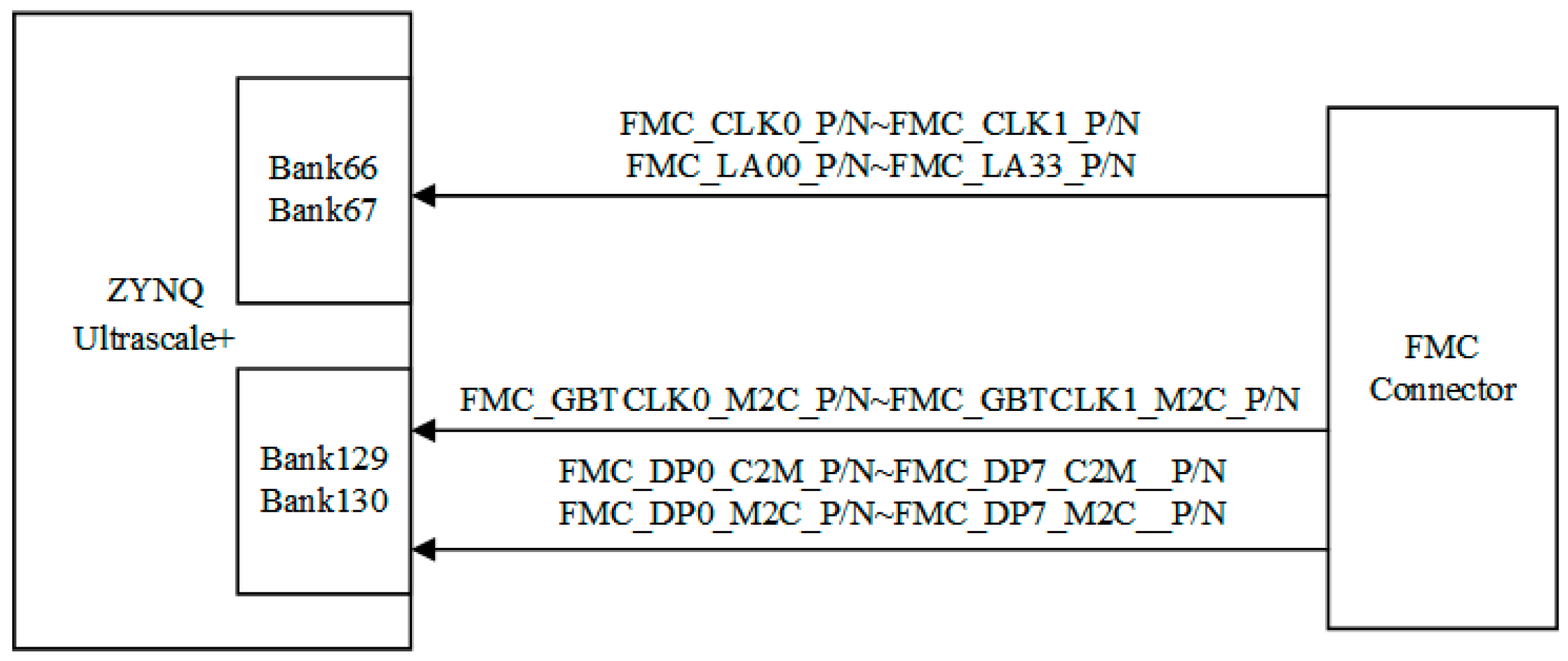
3.4. FMC Connector Circuit
This design will be equipped with an expansion connector to integrate boards with new functionalities. The connector should feature multiple available I/O interfaces, support for a wide range of signaling standards, high-speed signal transmission (up to 10 Gbit/s), and system-configurable input/output capabilities. Therefore, it has been decided to adopt a standard FMC HPC expansion connector as the solution for connecting ADC modules, ST interfaces, and other functional modules. This FMC expansion connector contains 36 pairs of differential I/O signals and supports LVDS data communication, making it capable of meeting diverse application requirements. A connection diagram for the FMC connector is shown in
Figure 9.
4. Clock Synchronization Module Design
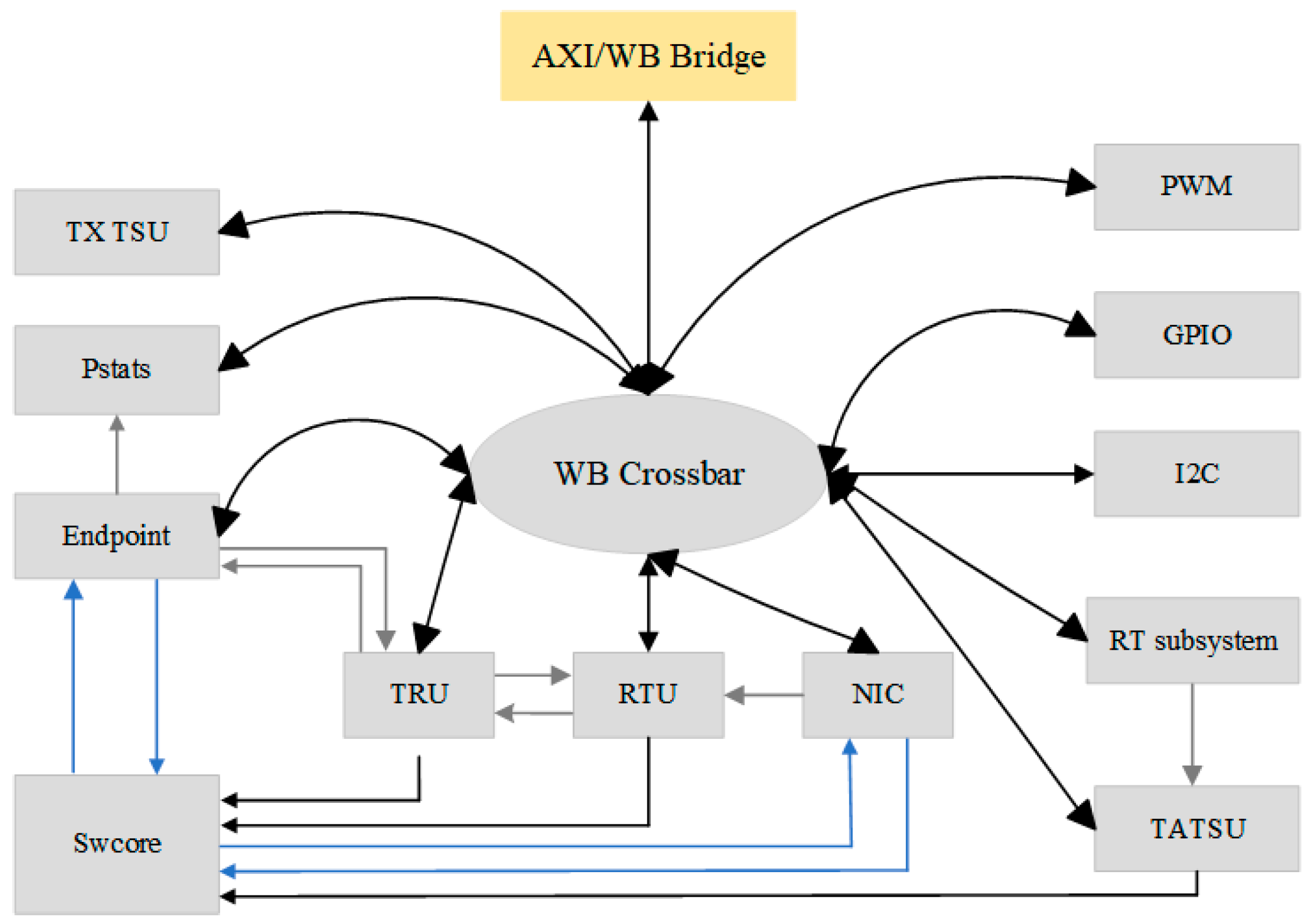
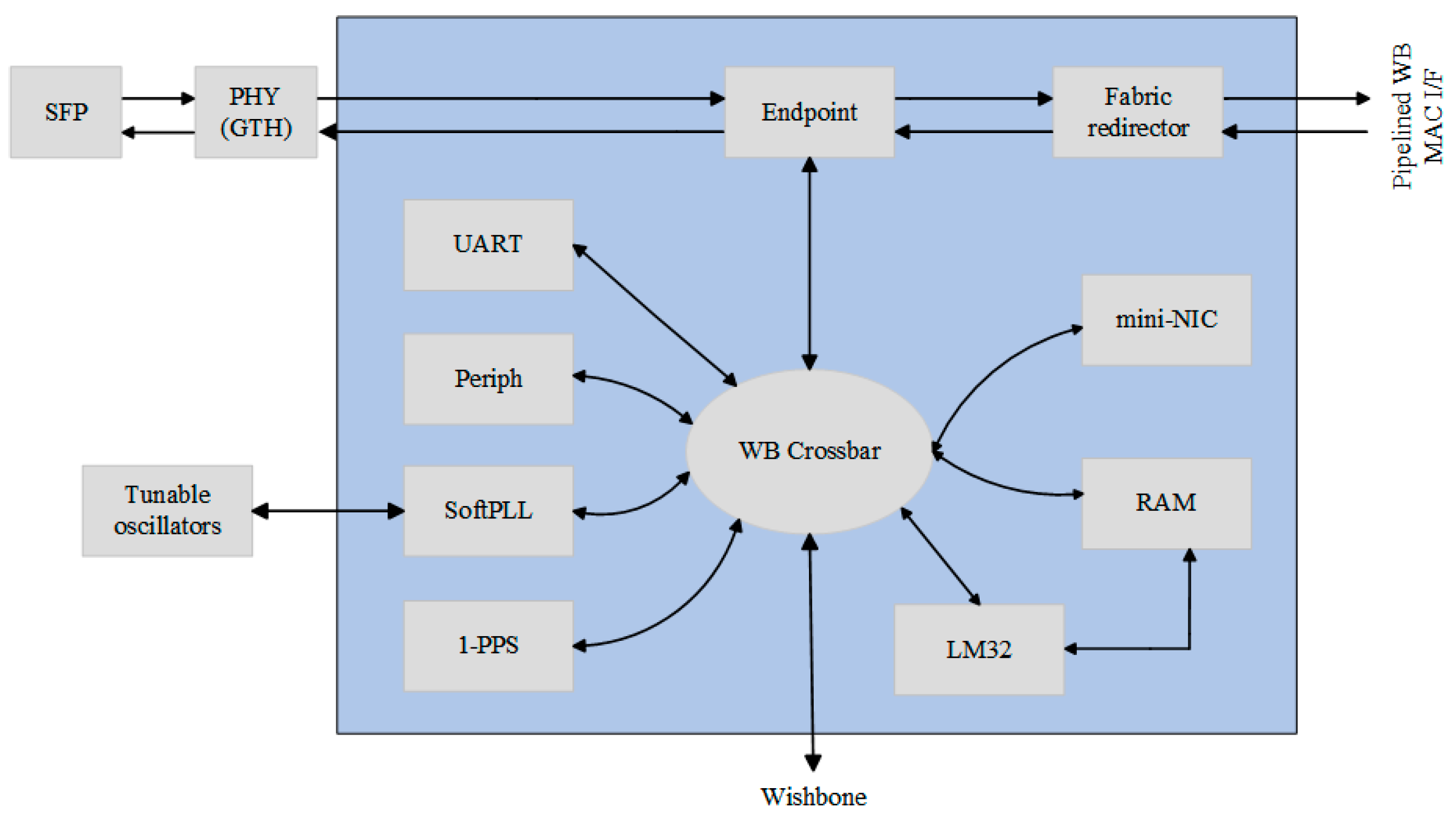
The top-level HDL design architecture of the time synchronization module is shown in
Figure 10. It mainly consists of multiple modules connected to the Wishbone Crossbar, with each module having a Wishbone bus interface and several registers. The CPU can perform read and write operations on these registers through the AXI interface. The blue arrows in the figure represent the transmission of Ethernet frames between the Endpoint, Swcore, and NIC.
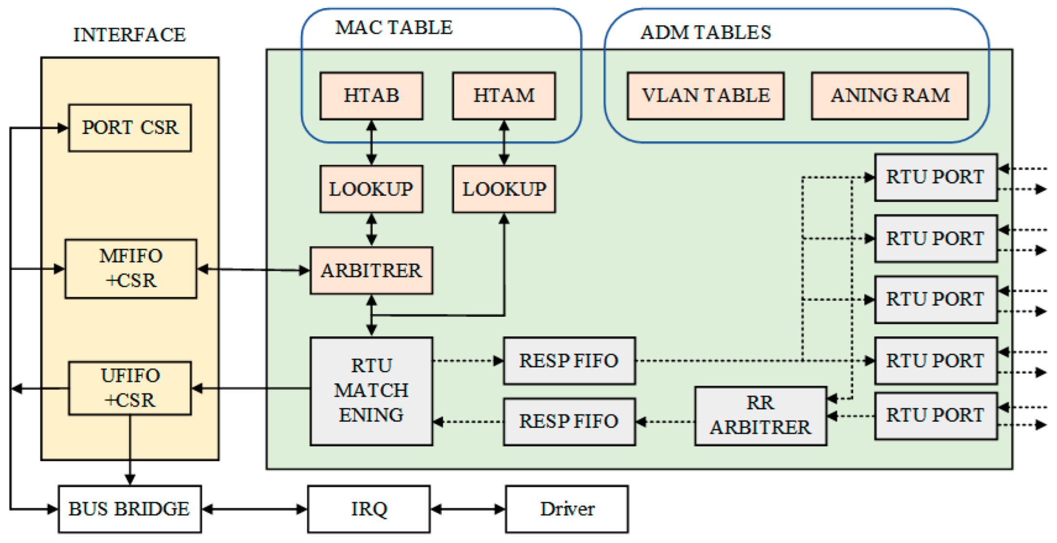
4.1. RTU Module
The RTU module is responsible for determining which port to forward each frame of data received from any port. The RTU consists of two parts: hardware and software. The hardware portion of the RTU is responsible for the switching process, while the software portion is responsible for the learning and aging processes, managing the filtering database and VLAN table, as shown in
Figure 11 and
Figure 12.
The main processes of the RTU are as follows:
(1) The RTU performs initialization.
(2) The hardware portion of the RTU receives the Protocol Data Unit (PDU) sent from the source MAC address to the destination MAC address.
(3) If the source MAC address is not in the MAC table, the hardware portion of the RTU will place an “Unrecognized Request” into the learning queue (UFIFO) and trigger a remote RTU interrupt.
(4) If the destination MAC address is not in the MAC table, the hardware portion of the RTU will broadcast the received PDU on every port except the receiving port while placing an “Unrecognized Request” into the user UFIFO and triggering a remote RTU interrupt.
(5) The software portion of the RTU’s learning process captures the remote RTU interrupt and reads the “Unrecognized Request” from the learning queue.
(6) The software portion of the RTU creates a filtering entry in the filtering database.
(7) The aging process of the RTU software portion tracks the duration of existence for each entry.
When an entry has existed for too long, the aging process of the RTU software portion will remove that entry from the filtering database.
4.2. NIC Module
The NIC module is responsible for transmitting Ethernet frames between the Linux system running on the PS side and the SFP interface on the PL side. It includes a frame buffer and two RAM blocks (TX descriptor memory and RX descriptor memory), which are used to store the descriptors of received frames and frames to be transmitted. The frame buffer stores all frames received from the physical port of the switch, as well as frames that the CPU intends to send to the switch port.
When the software running on the CPU wants to send an Ethernet frame, it must first write the frame into the frame buffer and then store the TX descriptor describing this frame in the TX descriptor memory. Conversely, the software must first write an empty RX descriptor into the RX descriptor memory. It must describe the offset and length of the area in the frame buffer where the NIC module can store the received frames. When a new frame is received, the NIC module will fill the RX descriptor and set the empty space to 0.
4.3. TX TSU Module
The TX TSU module collects the TX timestamps of Ethernet frames sent from all available endpoints in the switch. These timestamps are stored inside a FIFO queue and can be retrieved by the software running on the CPU, along with the frame ID (FID) and port ID (PID). The CPU uses this additional information to link the timestamps with the corresponding frames sent through the NIC module and one (or more) endpoints.
4.4. RT Subsystem Module
The internal structure of the RT Subsystem module is shown in
Figure 13.
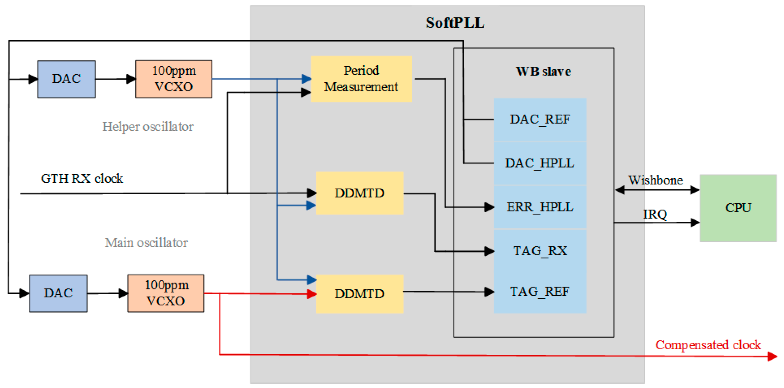
The function of the SoftPLL module is to synchronize the local 62.5 MHz reference clock with the RX clock recovered from the data stream. It consists of two phase-locked loops: the auxiliary phase-locked loop and the main phase-locked loop. The structure of the SoftPLL is shown in
Figure 14.
The SoftPLL module uses two externally tuned VCXOs controlled by DACs. The first DAC is responsible for generating a 62.5 MHz main reference clock to synchronize with the RX clock by adjusting the DDMTD offset frequency to bring it closer to the frequency of the RX clock recovered from the data stream. The second DAC outputs an auxiliary clock for the DDMTD. Both DACs are controlled via a Wishbone bus interface. The period measurement module is a linear frequency detector used to correctly set the DDMTD offset frequency based on the RX clock recovered from the data stream. Its implementation is based on a set of counters that periodically output the frequency error to the Wishbone bus interface. When the DDMTD offset clock is slower than the RX recovered clock, the generated value is positive; otherwise, when the DDMTD clock is faster than the RX recovered clock, the value is negative.
The 1-PPS module is responsible for generating and inputting the 1-PPS signal. It contains two time counters: cntr_utc and cntr_nsec. The cntr_utc is used to record the whole seconds of the WR time, while the cntr_nsec is used to record the fractional part of each second. The cntr_nsec is clocked with a 62.5 MHz reference clock, which provides a resolution of 16 ns. At the beginning of each second, the value of cntr_nsec is 0.
The Wishbone registers of the 1-PPS allow modifications to the cntr_utc and cntr_nsec counters. This can be accomplished in two ways: first, by setting the time, which directly stores a new value to the counters upon request; second, by adjusting the time, which means adding new values to the current state of both counters at the beginning of a new second.
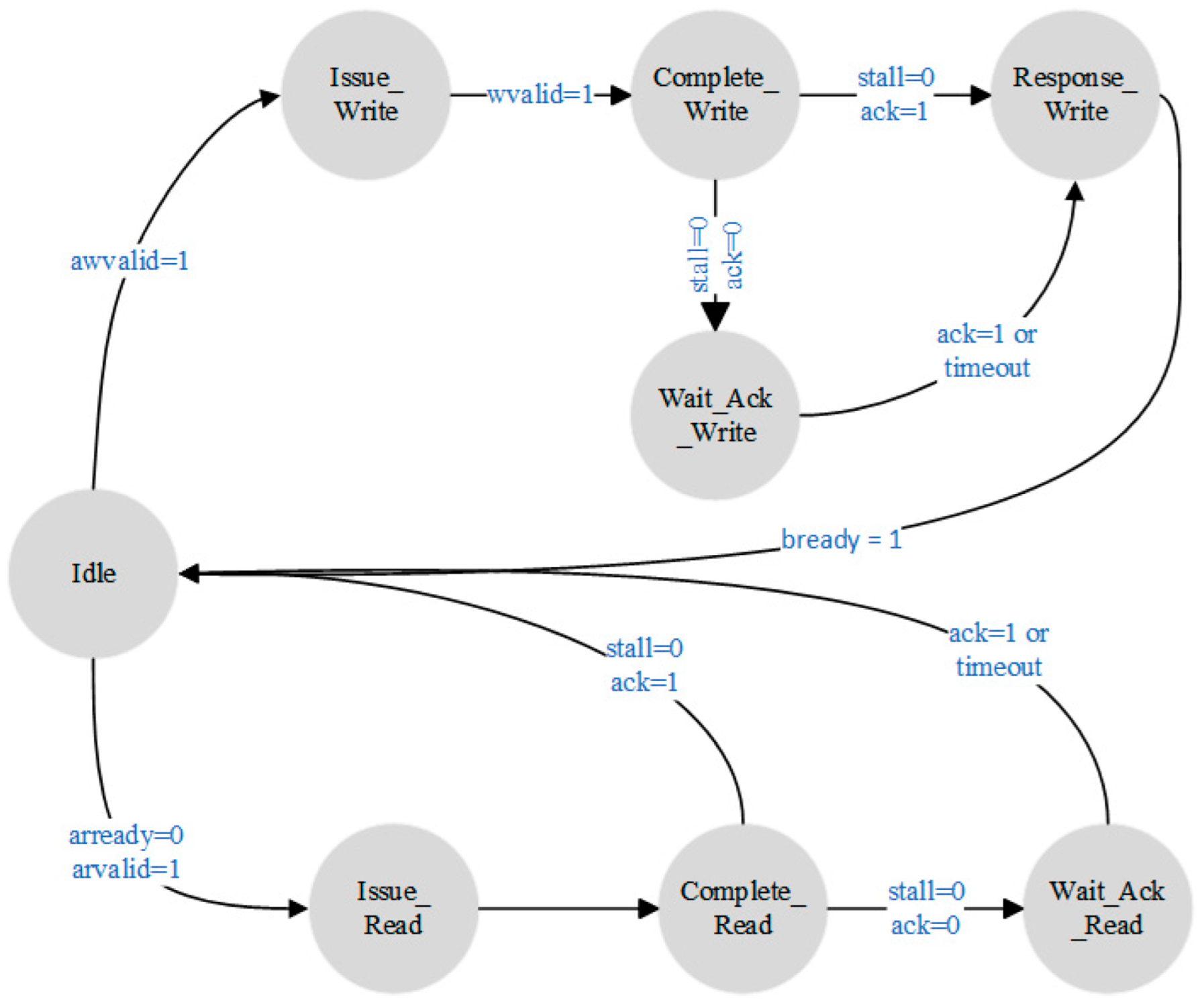
4.5. AXI to Wishbone Bridge (AXI-WB Bridge)
The various modules in the PL domain communicate via the Wishbone bus. Since the PS and PL domains of the Zynq communicate through the AXI bus, an AXI-to-Wishbone bridge is required to facilitate communication between the PS domain and the modules in the PL domain.
Data can be directly transmitted between the AXI bus and the Wishbone bus without the need for additional registers. The PL domain is connected to Zynq’s AXI interface as an AXI IP core, and the actual address of each module is the base address of the AXI interface (0 × 80000000) plus the offset address of that module.
When the AXI bus’s arready signal is 0 and the arvalid signal is 1, the read process is initiated. Data can only be transferred from the Wishbone bus to the AXI bus when the Wishbone bus’s stall signal is 0 and the ack signal is 1. When the AXI bus’s awvalid signal is 1, the write process begins, and when the AXI bus’s wvalid signal is 1, the data will be sent from the AXI bus to the Wishbone bus. The specific process is illustrated in
Figure 15.
5. Test Results
5.1. AXI-WB Communication Test
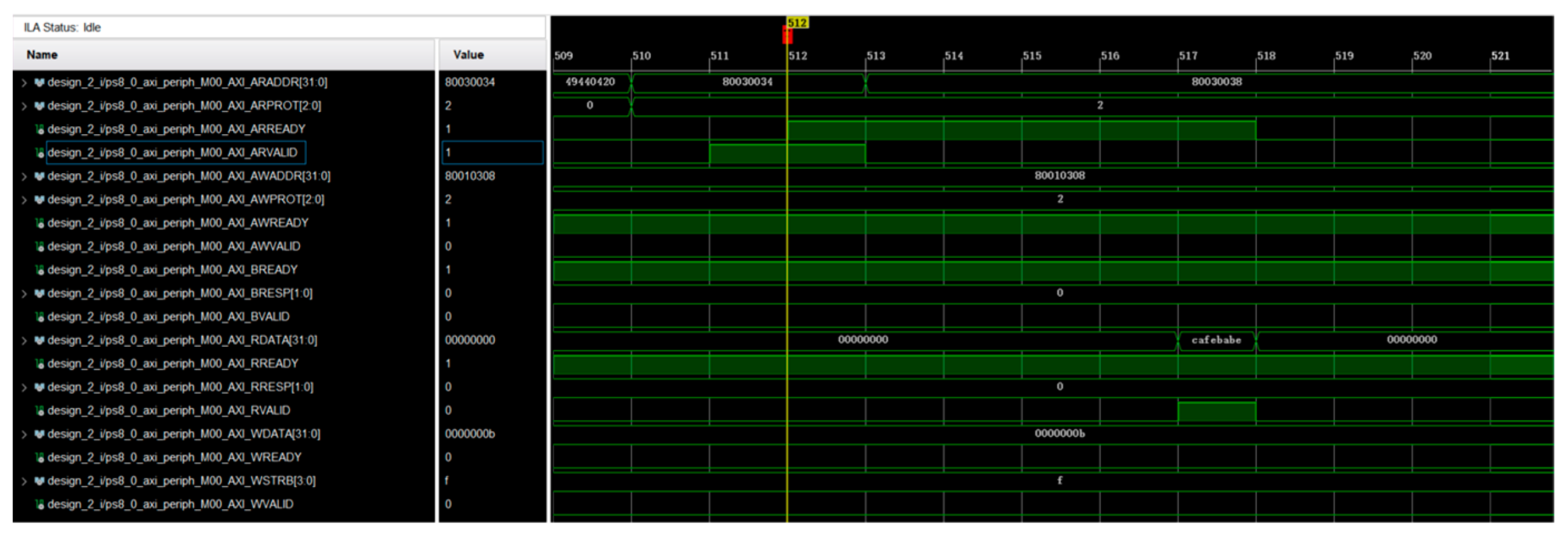
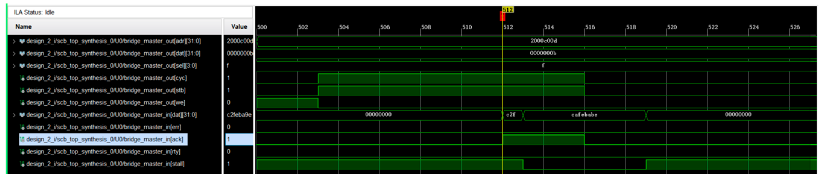
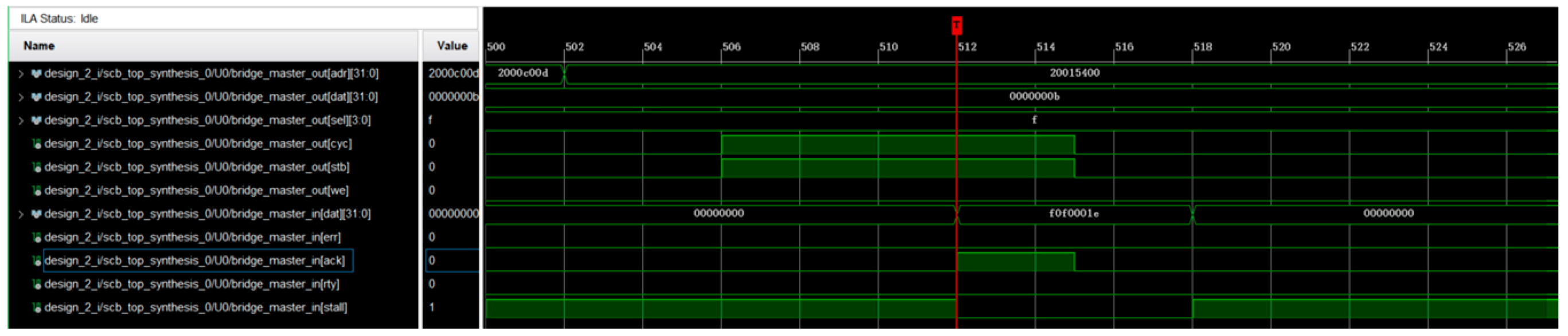
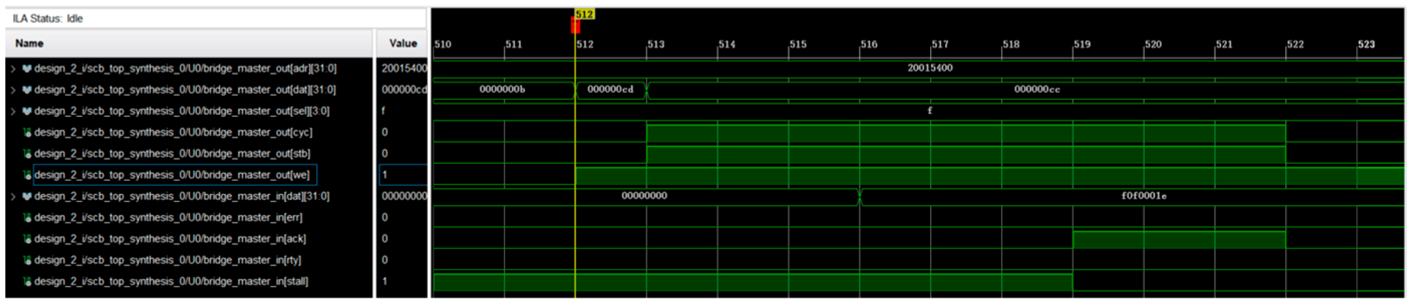
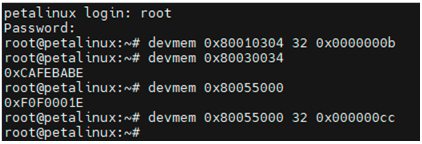
Since the reset signals of the various modules in the PL domain are controlled by the GPIO module in the RT Subsystem, it is necessary to first write the data 0 × 80010304 to this module to reset the system. In the read process test, the devmem tool is used in the Linux system to read the data at address 0 × 80030034 (Endpoint module), resulting in 0 × cafebabe. The processes on the AXI side and the Wishbone side are captured using ILA, as shown in
Figure 16 and
Figure 17. Next, the data from the PWM module are read, and the results are shown in
Figure 18 and
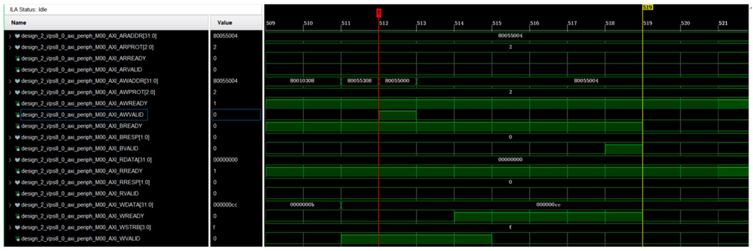
Figure 19. The results of both read processes are consistent with the data in the hardware logic, indicating that the read process is correct. In the write process test, the value 0 × 000000cc is written to the PWM module, and the test results are shown in
Figure 20 and
Figure 21. After multiple read and write tests, no hang-up issues were encountered, indicating that the write process was correct. The specific command used for the operation is shown in
Figure 22.
5.2. Formatting of Mathematical Components
Configure one of the ports as WR Slave mode, responsible for receiving and calibrating external synchronization signals, while the remaining ports are configured as WR Master mode, used to send synchronization signals to external devices, allowing the entire WR network to achieve synchronization.
Connect the switch to the WR Node device using a 5 m optical fiber, and then connect the WR Node to the PC via a USB interface. Use the serial tool MobaXterm to debug the ports. By typing the synchronization command “gui” in the terminal and pressing Enter, the transmission of time data can be completed. The specific test results are shown in
Figure 23.
From the figure, it can be observed that the synchronization time can be accurately matched to the specific test time, which is Fri, 17 January 2025, 19:55:37. The results indicate that the time synchronization precision can reach the sub-nanosecond level.
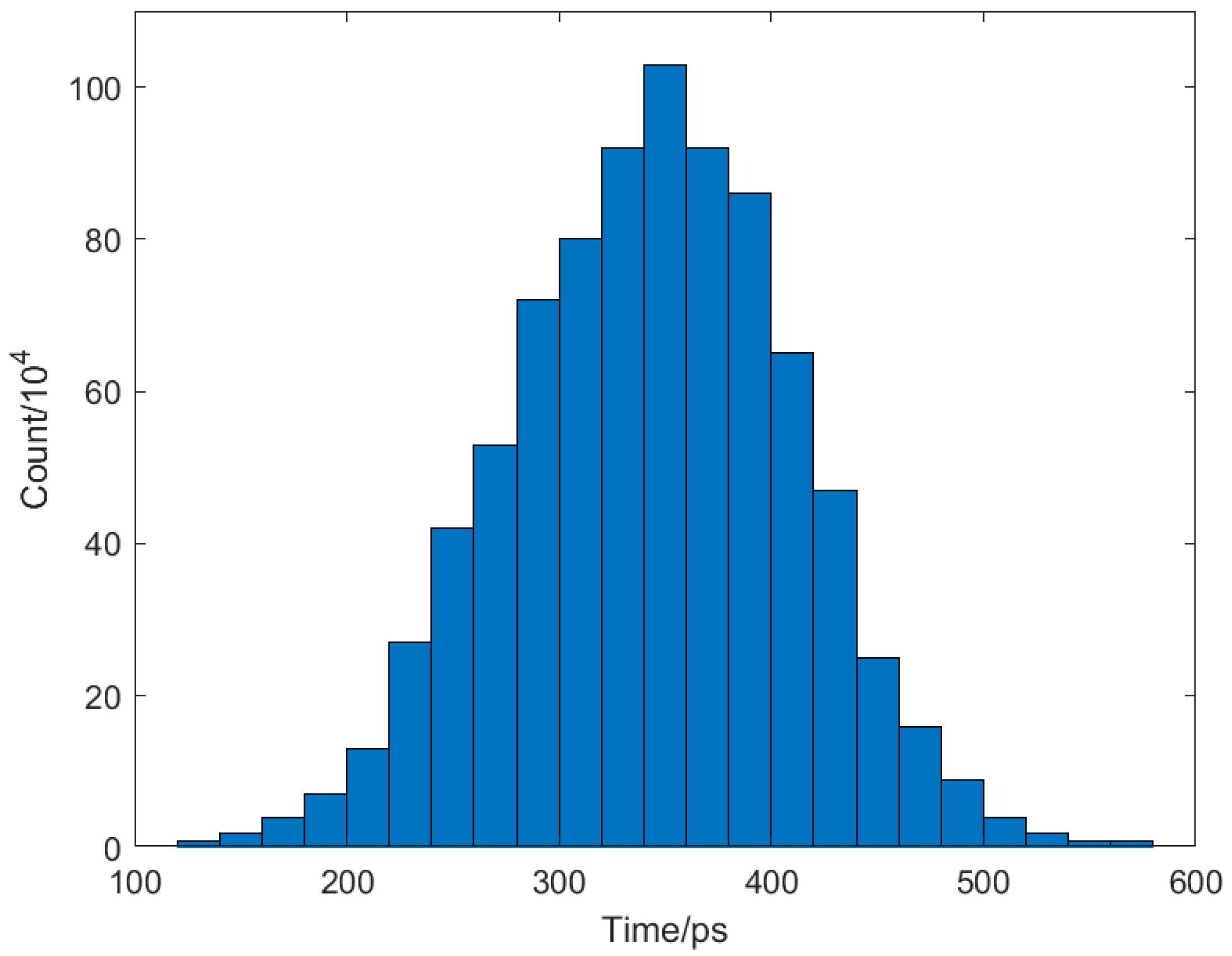
5.3. Synchronization Performance Test
Connect the switch to the WR Node and also route the PPS signals from both to the time-to-digital converter, which measures the precision of the second pulse. The test results are shown in
Figure 24. From the figure, it can be seen that the test results follow a normal distribution pattern, with a mean synchronization error of 33.76 ps. The time synchronization precision reaches the sub-nanosecond level, meeting the current environmental demands for time synchronization. Ref. [
24] introduces a dual-port device with WR functionality, whose PPS deviation has a mean value of approximately 129 ps, while reference [
25] describes a TSN switch that does not have WR functionality, with its PPS deviation in the 20 ns range.
6. Conclusions
In this paper, a time synchronization switch based on the Zynq platform is proposed. It mainly discusses the design of the hardware schematic, the time synchronization module, and the AXI-WB Bridge. Additionally, AXI communication testing, time synchronization functionality, clock jitter, and synchronization performance tests were completed in the experimental environment. The test results indicate that the PS side can cyclically read from and write to the various modules on the PL side, and the instantaneous precision of time synchronization can reach the sub-nanosecond level. This makes it suitable for distributed systems with high time synchronization requirements. The use of the GTH interface this time will provide faster transmission speeds compared to the previously used GTX interface, while also reducing the physical size. Additionally, by utilizing the development tools provided by Xilinx, the development efficiency has been further improved. Next, two aspects need to be expanded. Firstly, there are plans to enhance the functionality of the existing switch by adding an ID allocation feature, which will assign a unique identifier to each slave device and incorporate it into the time synchronization protocol to achieve time synchronization across the entire network. At the same time, data aggregation capability will be increased, allowing the switch to collect data from the ADC board. Secondly, research is needed on how to modify the configuration of the GTH module and the time synchronization algorithm to further improve time synchronization accuracy.
Author Contributions
Conceptualization, Y.M.; methodology, Y.M. and R.H.; software, R.H. and Z.W.; investigation, J.L.; data curation, J.L.; writing—original draft preparation, R.H.; writing—review and editing, Y.M., R.H., Z.W. and J.L.; supervision, Y.M. All authors have read and agreed to the published version of the manuscript.
Funding
This research received no external funding.
Institutional Review Board Statement
Not applicable.
Informed Consent Statement
Not applicable.
Data Availability Statement
Data are contained within the article.
Conflicts of Interest
The authors declare no conflicts of interest.
References
- Tratnik, J.; Pavlovic, L.; Batagelj, B.; Lemut, P.; Ritosa, P.; Ferianis MVidmar, M. Fiber length compensated transmission of 2998.01 MHz RF signal with femtosecond precision. Microw. Opt. Technol. Lett. 2011, 53, 1553–1555. [Google Scholar] [CrossRef]
- Alshaikhli, A.O.; Rhee, J.M. TFR: A Novel Approach for Clock Synchronization Fault Recovery in Precision Time Protocol (PTP) Networks. Appl. Sci. 2018, 8, 21. [Google Scholar] [CrossRef]
- Xu, C.; Li, B. Design of noc router based on high speed data acquisition. Microelectron. Comput. 2017, 34, 140–144. [Google Scholar]
- Mills, D. Computer Network Time Synchronization: The Network Time Protocol on Earth and in Space, 2nd ed.; CRC Press: Boca Raton, FL, USA, 2017. [Google Scholar]
- Zhao, L.; He, F.; Li, E.; Lu, J. Comparison of Time Sensitive Networking (TSN) and TTEthernet. In Proceedings of the 2018 IEEE 37th Digital Avionics Systems Conference, London, UK, 23–27 September 2018; pp. 1–7. [Google Scholar]
- Subrahmanyan, R. Implementation considerations for IEEE 1588v2 applications in telecommunications. In Proceedings of the 2007 IEEE International Symposium on Precision Clock Synchronization for Measurement, Control and Communication, Vienna, Austria, 1–3 October 2007; pp. 148–154. [Google Scholar]
- Real, D.; Calvo, D. White Rabbit Expansion Board: Design, Architecture, and Signal Integrity Simulations. Electronics 2023, 12, 3394. [Google Scholar] [CrossRef]
- Ring, F.; Exel, R.; Muller, T. Control loop optimization—Knowing your environment. In Proceedings of the 2014 IEEE International Symposium on Precision Clock Synchronization for Measurement, Control, and Communication (ISPCS), Austin, TX, USA, 22–26 September 2014; pp. 77–82. [Google Scholar]
- Lopez-Jimenez, J.; Jimenez-Lopez, M.; Diaz, J.; Gutierrez-Rivas, J.L. White-rabbit-enabled data acquisition system. In Proceedings of the 2017 Joint Conference of the European Frequency and Time Forum and IEEE International Frequency Control Symposium (EFTF/IFC), Besancon, France, 9–13 July 2017; pp. 410–416. [Google Scholar]
- Lan, Y.K.; Chen, Y.S.; Hou, T.C.; Wu, B.L.; Chu, Y.S. Development Board Implementation and Chip Design of IEEE 1588 Clock Synchronization System Applied to Computer Networking. Electronics 2023, 12, 2166. [Google Scholar] [CrossRef]
- Li, F.; Liu, W.; Qi, Y.; Li, Q.; Liu, G. An Enhanced Method for Nanosecond Time Synchronization in IEEE 1588 Precision Time Protocol. Processes 2023, 11, 1328. [Google Scholar] [CrossRef]
- Neelam; Olaniya, M.P.; Rathore, H.; Sharma, L.; Roy, A.; De, S.; Panja, S. Precise time synchronization and clock comparison through a white rabbit network-based optical fiber link. Radio Sci. 2021, 56, 1–9. [Google Scholar] [CrossRef]
- Hann, K.; Jobert, S.; Rodrigues, S. Synchronous ethernet to transport frequency and phase/time. IEEE Commun. Mag. Artic. News Events Interest Commun. Eng. 2012, 50, 152–160. [Google Scholar] [CrossRef]
- Moreira, P.; Alvarez, P.; Serrano, J.; Darwezeh, I.; Wlostowski, T. Digital dual mixer time difference for sub-nanosecond time synchronization in Ethernet. In Proceedings of the 2010 IEEE International Frequency Control Symposium, Newport Beach, CA, USA, 1–4 June 2010; pp. 449–453. [Google Scholar]
- Kaur, N.; Frank, F.; Pottie, P.E.; Tuckey, P. Time and frequency transfer over a 500 km cascaded White Rabbit network. In Proceedings of the 2017 Joint Conference of the European Frequency and Time Forum and IEEE International Frequency Control Symposium (EFTF/IFCS), Besancon, France, 9–13 July 2017; pp. 86–90. [Google Scholar]
- Ye, Y.; Li, H.; Li, J.; Yan, Y.; Yu, P.; Gong, G. Timing system based on customized frequency White Rabbit network in SHINE. J. Instrum. 2022, 17, 1748–1756. [Google Scholar] [CrossRef]
- Neelam; Rathore, H.; Sharma, L.; Roy, A.; Olaniya, M.; De, S.; Panja, S. Studies on Temperature Sensitivity of a White Rabbit Network-Based Time Transfer Link. MAPAN 2021, 36, 253–258. [Google Scholar] [CrossRef]
- Derviskadic, A.; Razzaghi, R.; Walger, Q.; Paolone, M. The White Rabbit time synchronization protocol for synchrophasor networks. IEEE Trans. Smart Grid 2020, 11, 726–738. [Google Scholar] [CrossRef]
- Aweya, J. Emerging Applications of Synchronous Ethernet in Telecommunication Networks. IEEE Circuits Syst. Mag. 2012, 12, 56–72. [Google Scholar] [CrossRef]
- Pini, M.; Minetto, A.; Vesco, A.; Berbecaru, D.; Contreras Murillo, L.M.; Nemry, P.; De Francesca, I.; Rat, B.; Callewaert, K. Satellite-derived Time for Enhanced Telecom Networks Synchronization: The ROOT Project. In Proceedings of the 2021 IEEE 8th International Workshop on Metrology for AeroSpace (MetroAeroSpace), Naples, Italy, 23–25 June 2021; pp. 288–293. [Google Scholar]
- Pini, M.; Minetto, A.; Nemry, P.; Rat, B.; Contreras Murillo, L.M.; De Francesca, I.; Margaria, D.; Vesco, A.; Berbecaru, D.; Callewaert, K.; et al. Protection of GNSS-based Synchronization in Communication Networks: The ROOT project. In Proceedings of the European Navigation Conference & International Navigation Conference (Navigation 2021), Virtual Event, 15–18 November 2021. [Google Scholar]
- Kim, H.J.; Lee, U.; Kim, M.; Lee, S. Time-Synchronization Method for CAN–Ethernet Networks with Gateways. Appl. Sci. 2020, 10, 8873. [Google Scholar] [CrossRef]
- Meng, C.; Xu, C.; Liao, J. Research on Clock Synchronization of Data Acquisition Based on NoC. Appl. Sci. 2024, 14, 4838. [Google Scholar] [CrossRef]
- Zhang, T. Integrated Time-Frequency Data Transmission Based on WR. Master’s Thesis, Guilin University of Electronic Technology, Guilin, China, 2022. [Google Scholar]
- Liu, Q.M. FPGA Design and Implementation of TSN Switch. Master’s Thesis, University of Electronic Science and Technology of China, Chengdu, China, 2023. [Google Scholar]
Figure 1.
Standard Ethernet and synchronous Ethernet.
Figure 1.
Standard Ethernet and synchronous Ethernet.
Figure 2.
PTP message exchange process.
Figure 2.
PTP message exchange process.
Figure 3.
The internal structure of the DDMTD.
Figure 3.
The internal structure of the DDMTD.
Figure 4.
The signal generated by the DDMTD.
Figure 4.
The signal generated by the DDMTD.
Figure 5.
Overall structure diagram.
Figure 5.
Overall structure diagram.
Figure 6.
DDMTD clock design.
Figure 6.
DDMTD clock design.
Figure 7.
GTH reference clock design.
Figure 7.
GTH reference clock design.
Figure 8.
SFP design block diagram.
Figure 8.
SFP design block diagram.
Figure 9.
FMC connector connection diagram.
Figure 9.
FMC connector connection diagram.
Figure 10.
Top-level HDL design architecture of the time synchronization module.
Figure 10.
Top-level HDL design architecture of the time synchronization module.
Figure 11.
RTU hardware block diagram.
Figure 11.
RTU hardware block diagram.
Figure 12.
Block diagram of the first version of the RTU software.
Figure 12.
Block diagram of the first version of the RTU software.
Figure 13.
The internal structure of the RT Subsystem module.
Figure 13.
The internal structure of the RT Subsystem module.
Figure 14.
The structure of the SoftPLL.
Figure 14.
The structure of the SoftPLL.
Figure 15.
Transmission process of AXI-WB.
Figure 15.
Transmission process of AXI-WB.
Figure 16.
Read Endpoint module via AXI bus.
Figure 16.
Read Endpoint module via AXI bus.
Figure 17.
Read Endpoint module via WB bus.
Figure 17.
Read Endpoint module via WB bus.
Figure 18.
Read PWM module via AXI bus.
Figure 18.
Read PWM module via AXI bus.
Figure 19.
Read PWM module via WB bus.
Figure 19.
Read PWM module via WB bus.
Figure 20.
Write data to PWM via AXI bus.
Figure 20.
Write data to PWM via AXI bus.
Figure 21.
Write data to PWM via WB bus.
Figure 21.
Write data to PWM via WB bus.
Figure 22.
Transfer command.
Figure 22.
Transfer command.
Figure 23.
Time synchronization interface.
Figure 23.
Time synchronization interface.
Figure 24.
PPS deviation test.
Figure 24.
PPS deviation test.
| Disclaimer/Publisher’s Note: The statements, opinions and data contained in all publications are solely those of the individual author(s) and contributor(s) and not of MDPI and/or the editor(s). MDPI and/or the editor(s) disclaim responsibility for any injury to people or property resulting from any ideas, methods, instructions or products referred to in the content. |
© 2025 by the authors. Licensee MDPI, Basel, Switzerland. This article is an open access article distributed under the terms and conditions of the Creative Commons Attribution (CC BY) license (https://creativecommons.org/licenses/by/4.0/).


