
Efficient Implementation of Polymer Microwave Fiber Links Employing Non-Galvanic Coupling Mechanism

 ,
,
Abstract
1. Introduction
2. PMF Overview
2.1. PMF Materials and Processes
2.2. PMF Propagation Characteristics
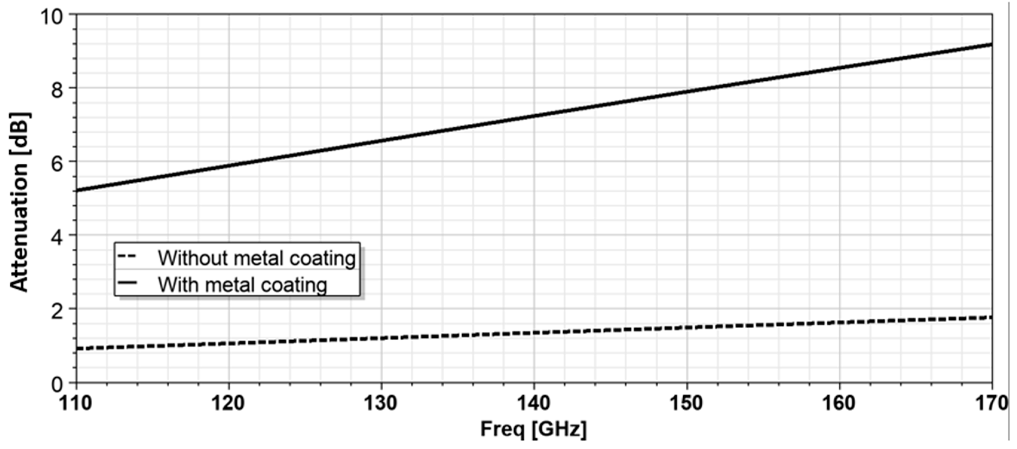
2.2.1. Attenuation
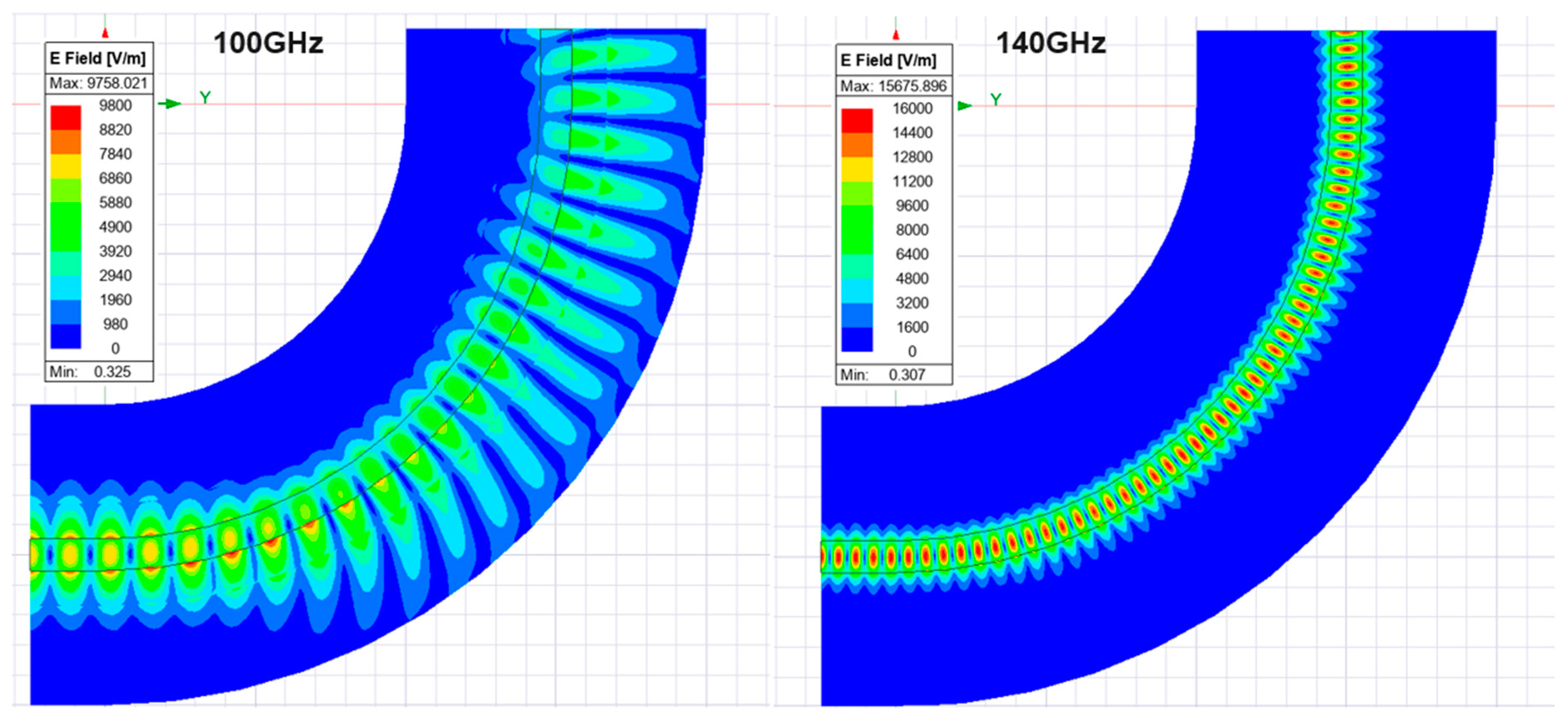
2.2.2. Dispersion
2.3. PMF Electrical Performance Simulation Results
3. PMF-AiP Coupling
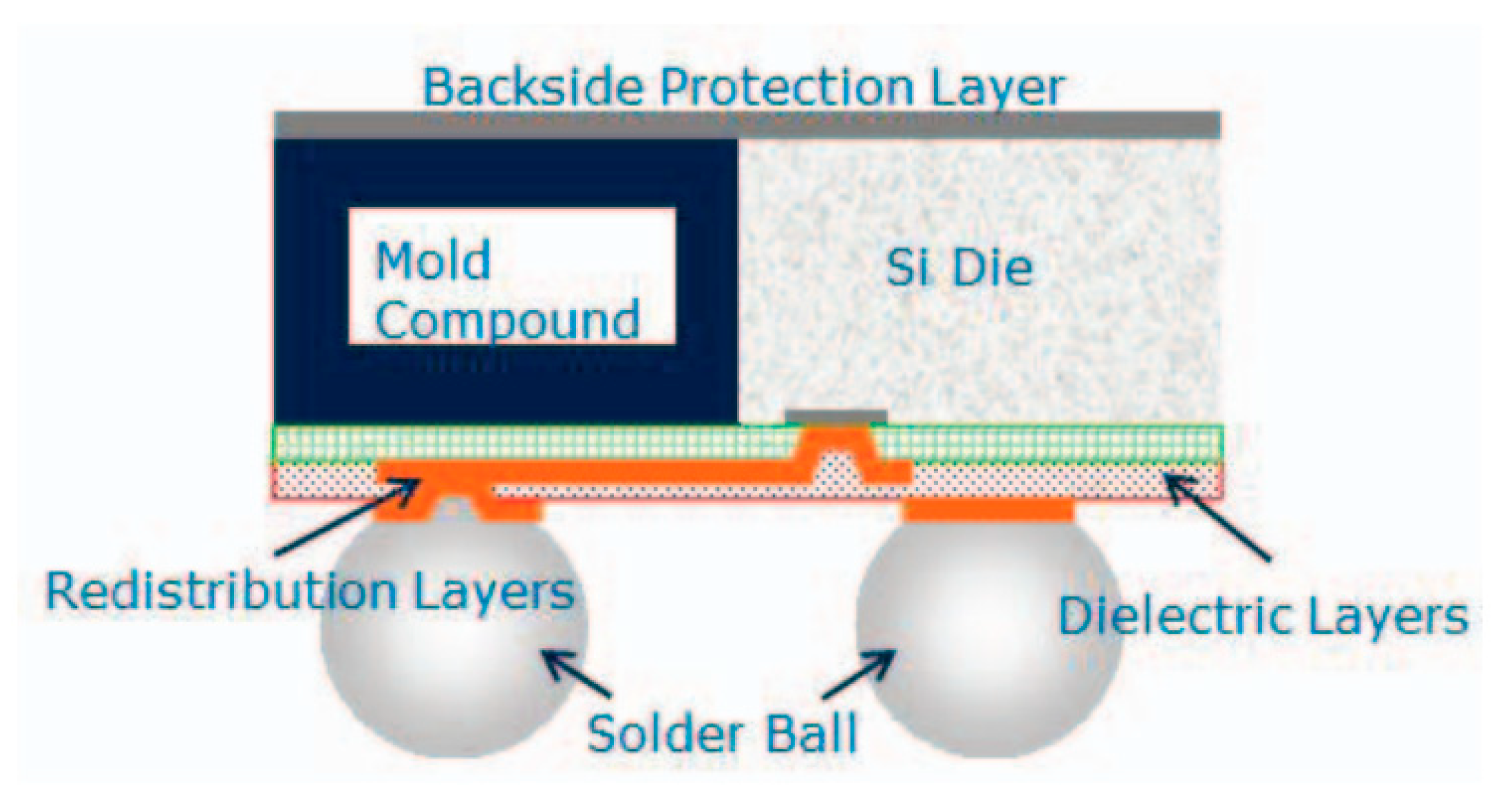
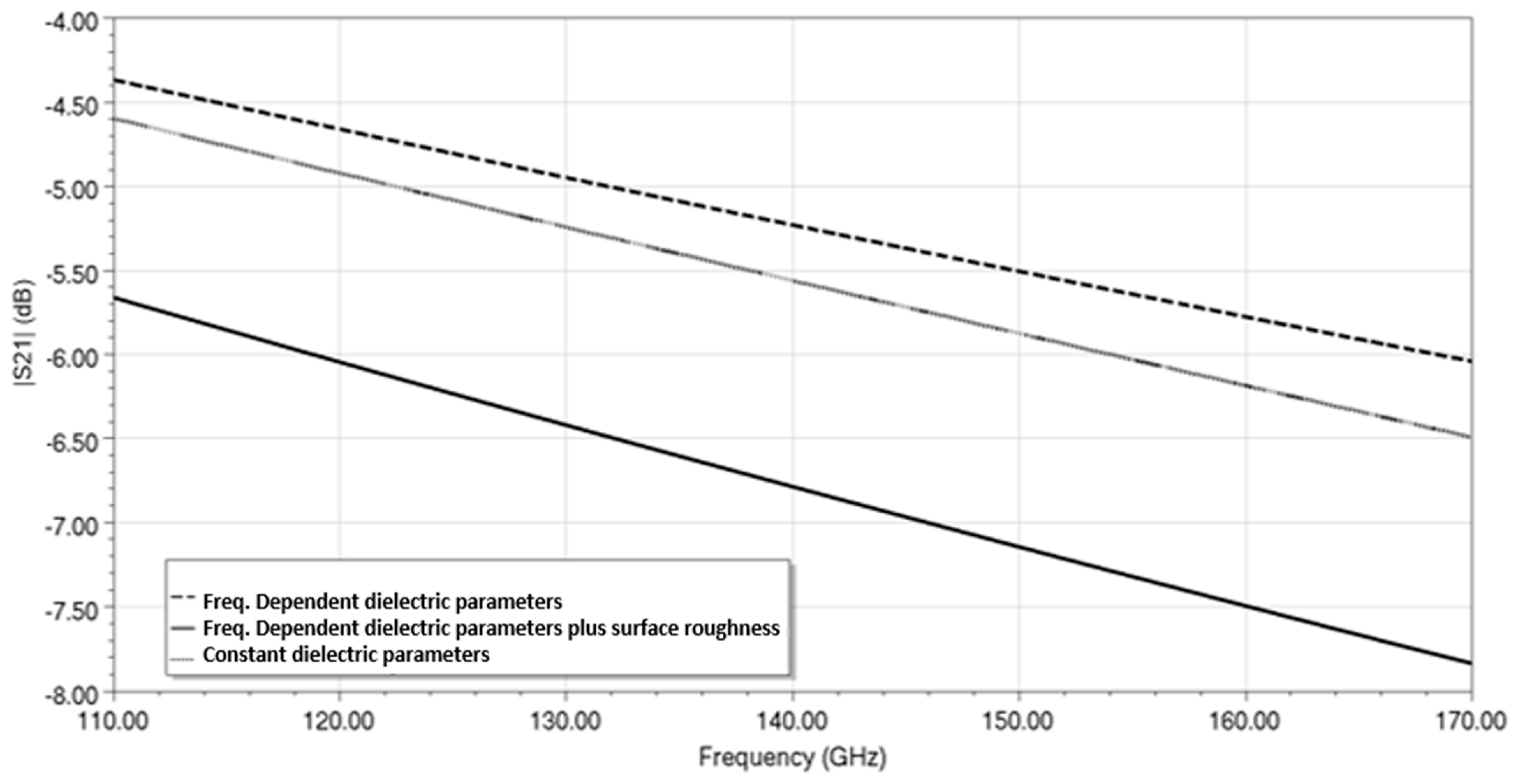
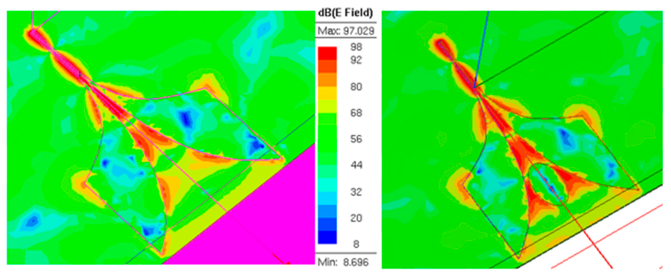
3.1. Packaging Technology Characterization
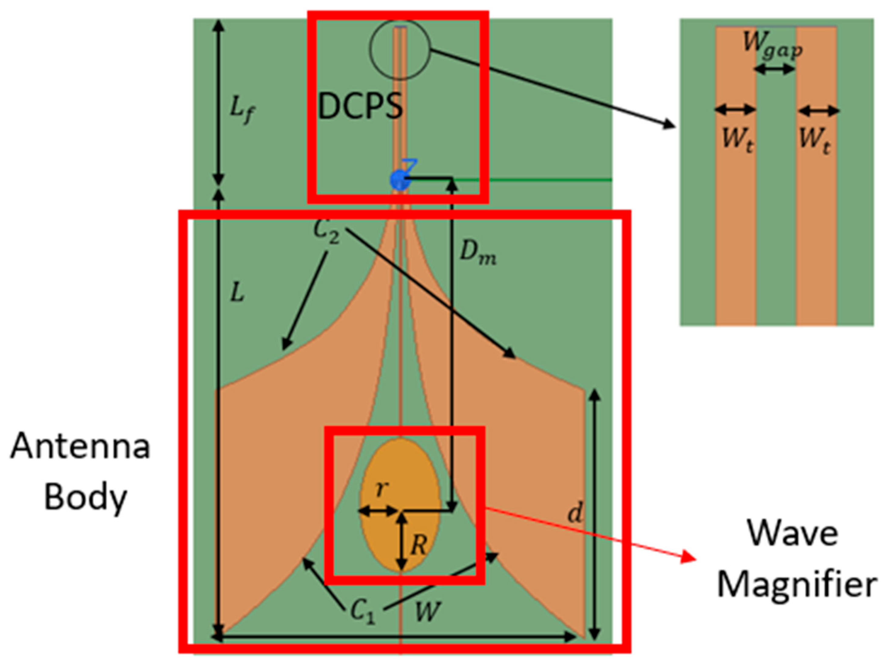
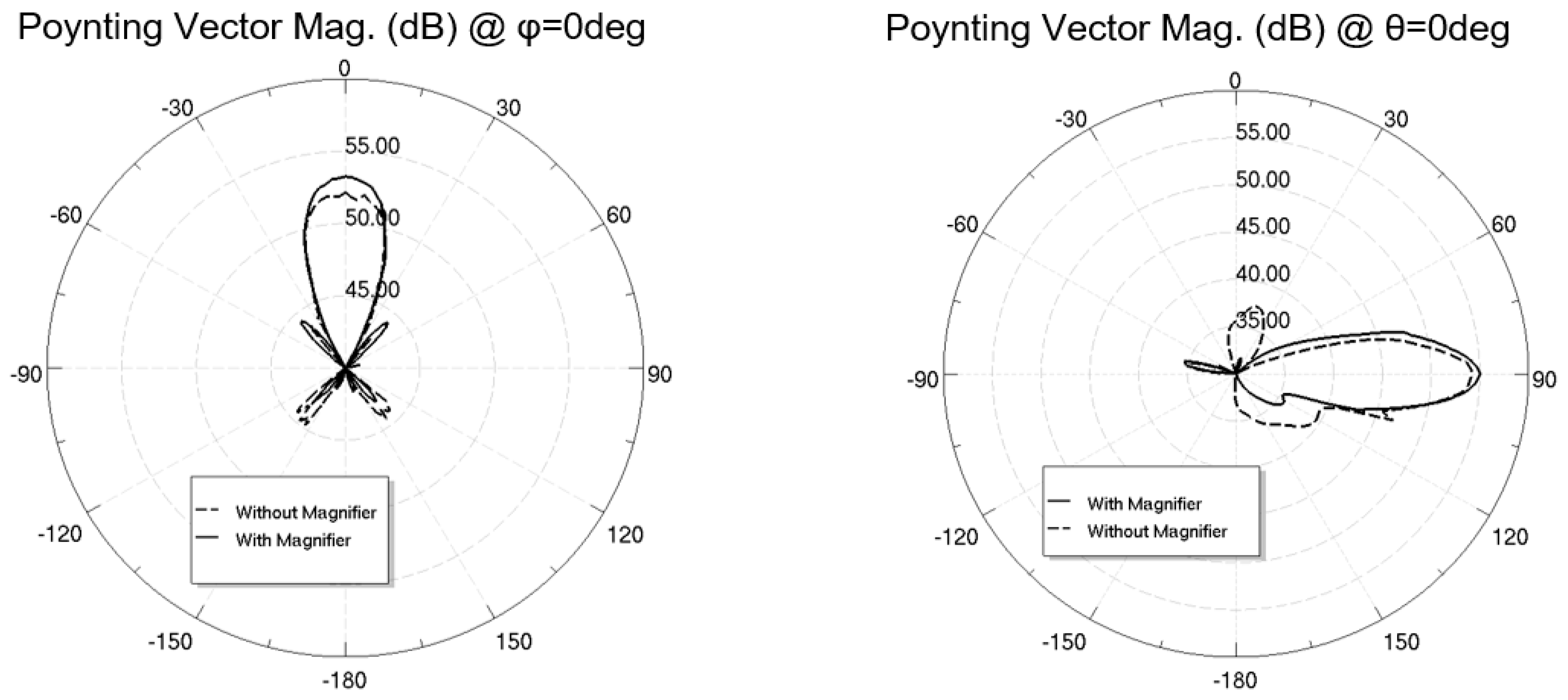
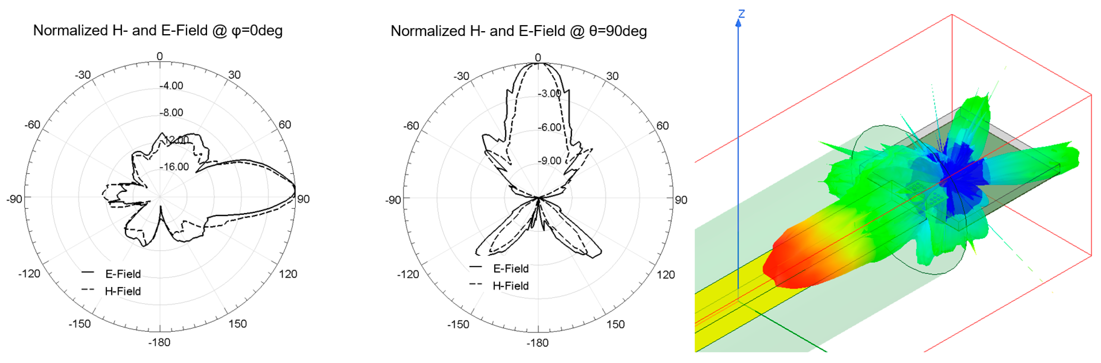
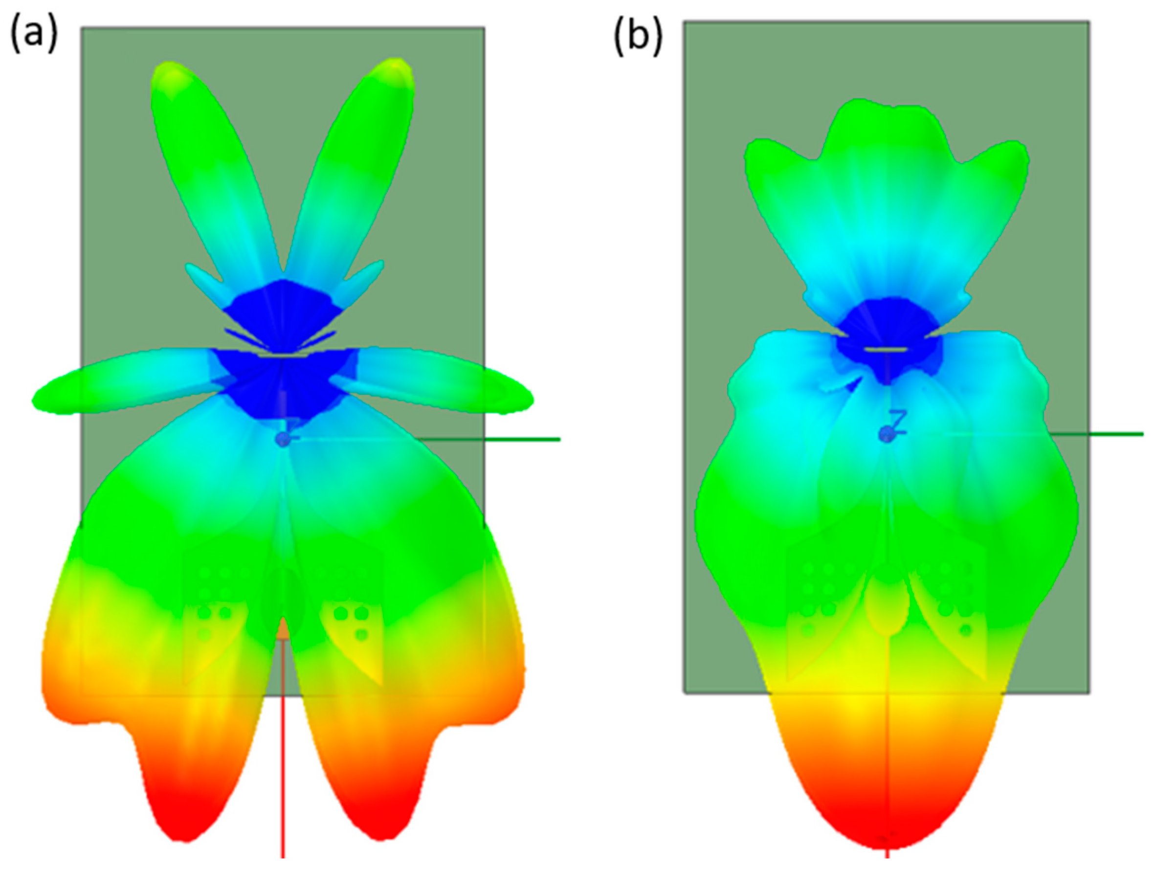
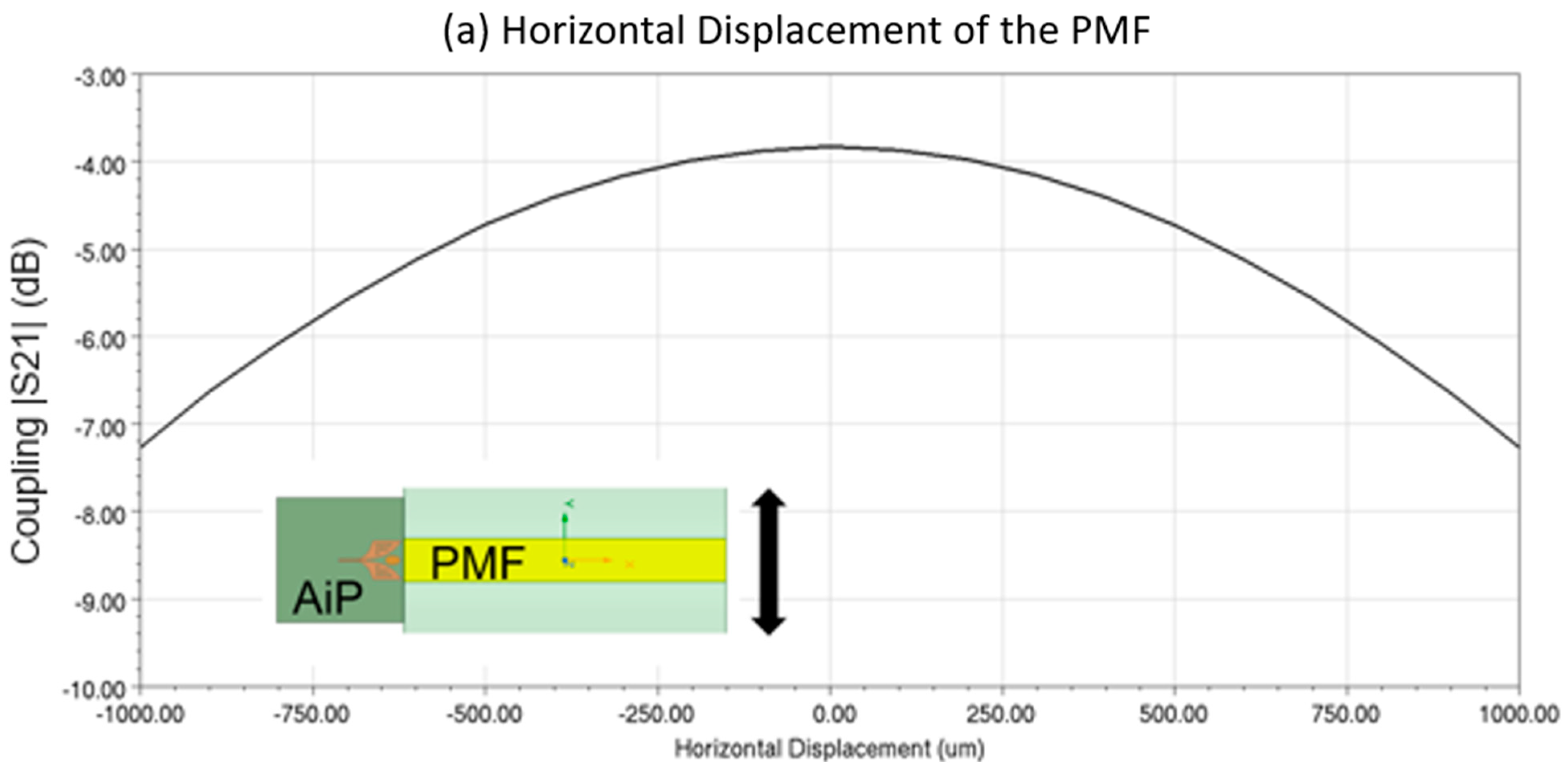
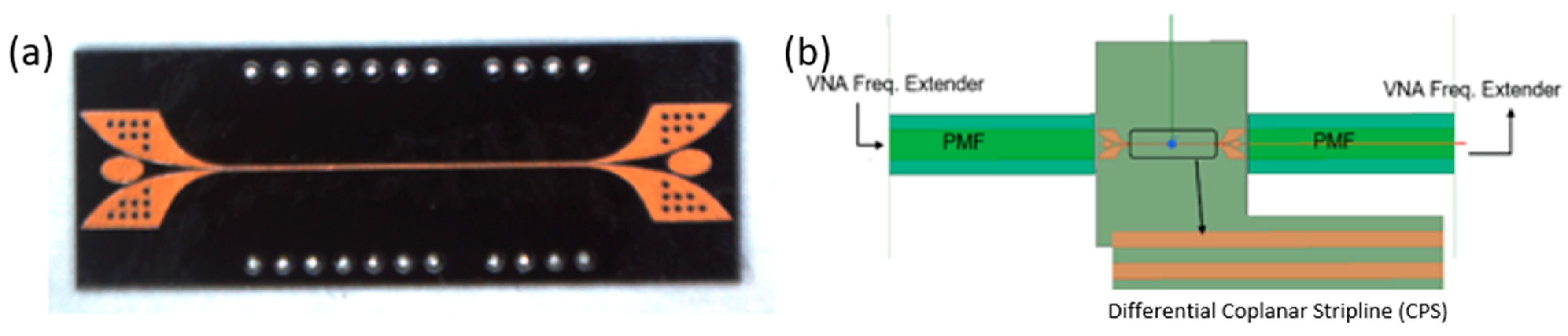
3.2. Coupler Design
4. AiP Implementation and Measurements
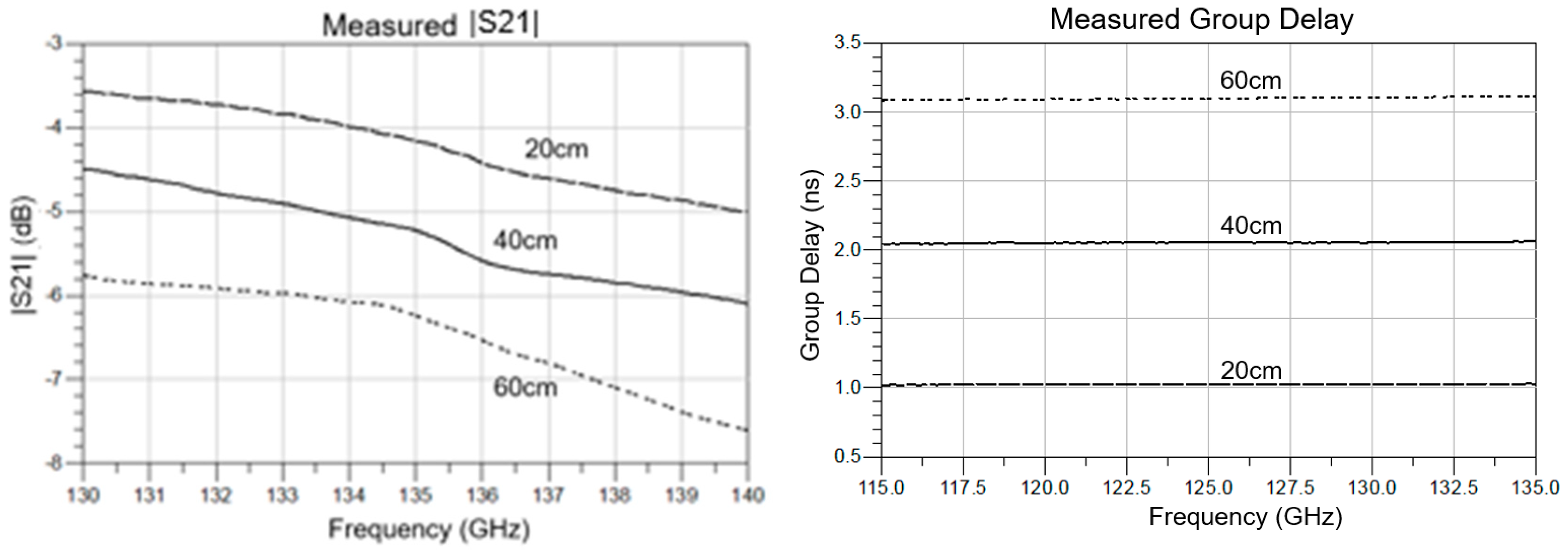
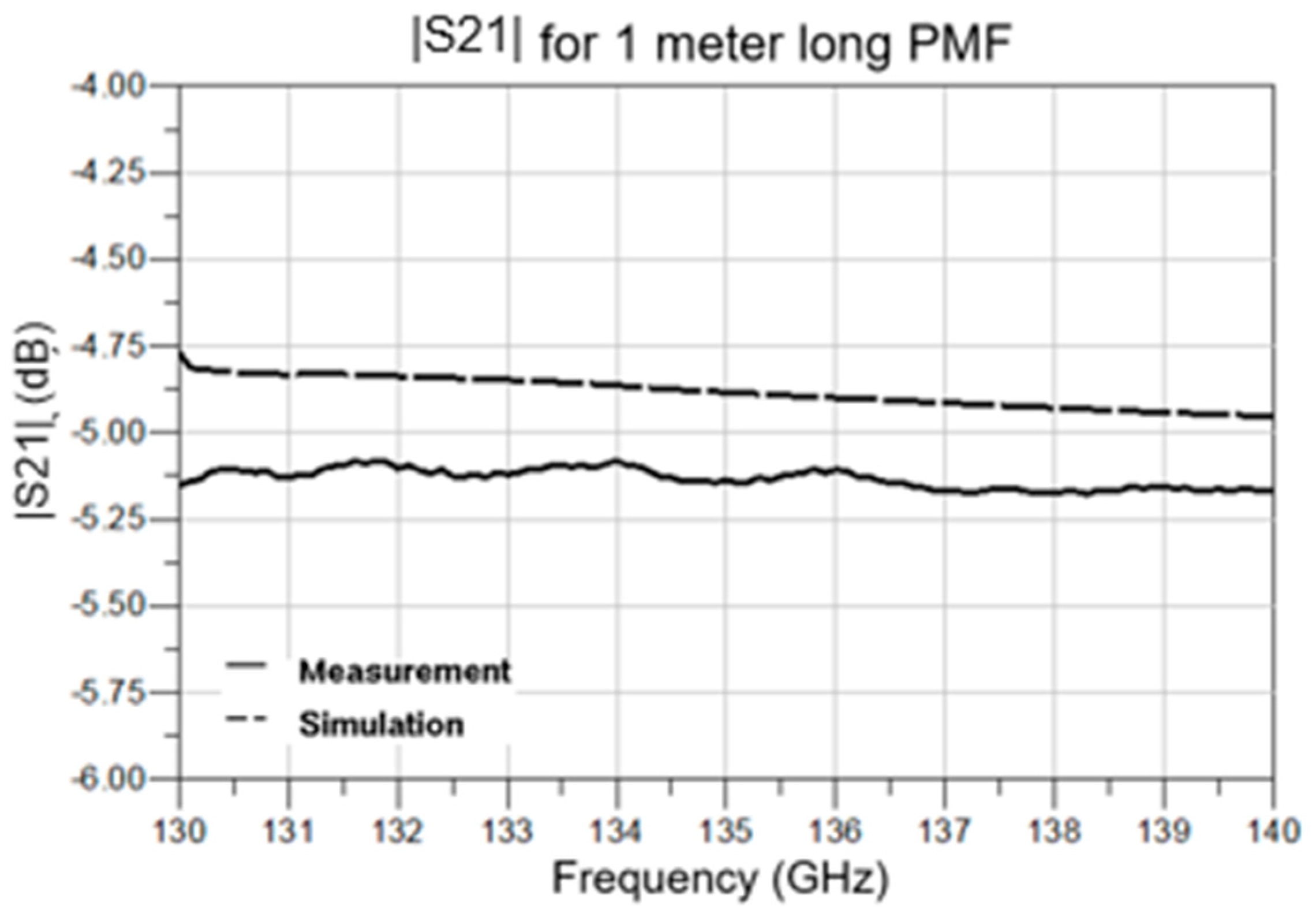
4.1. PMF Measurements
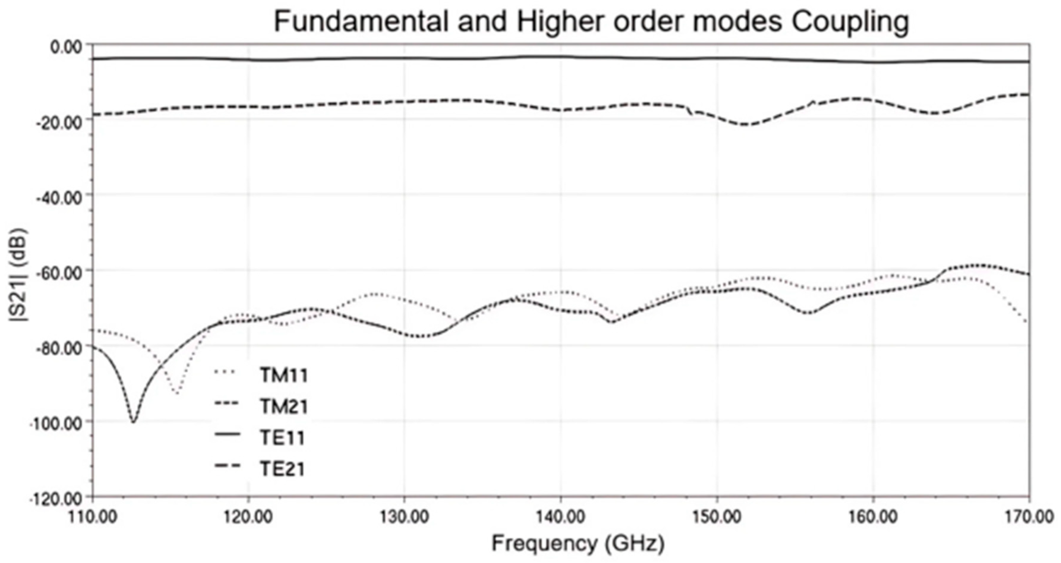
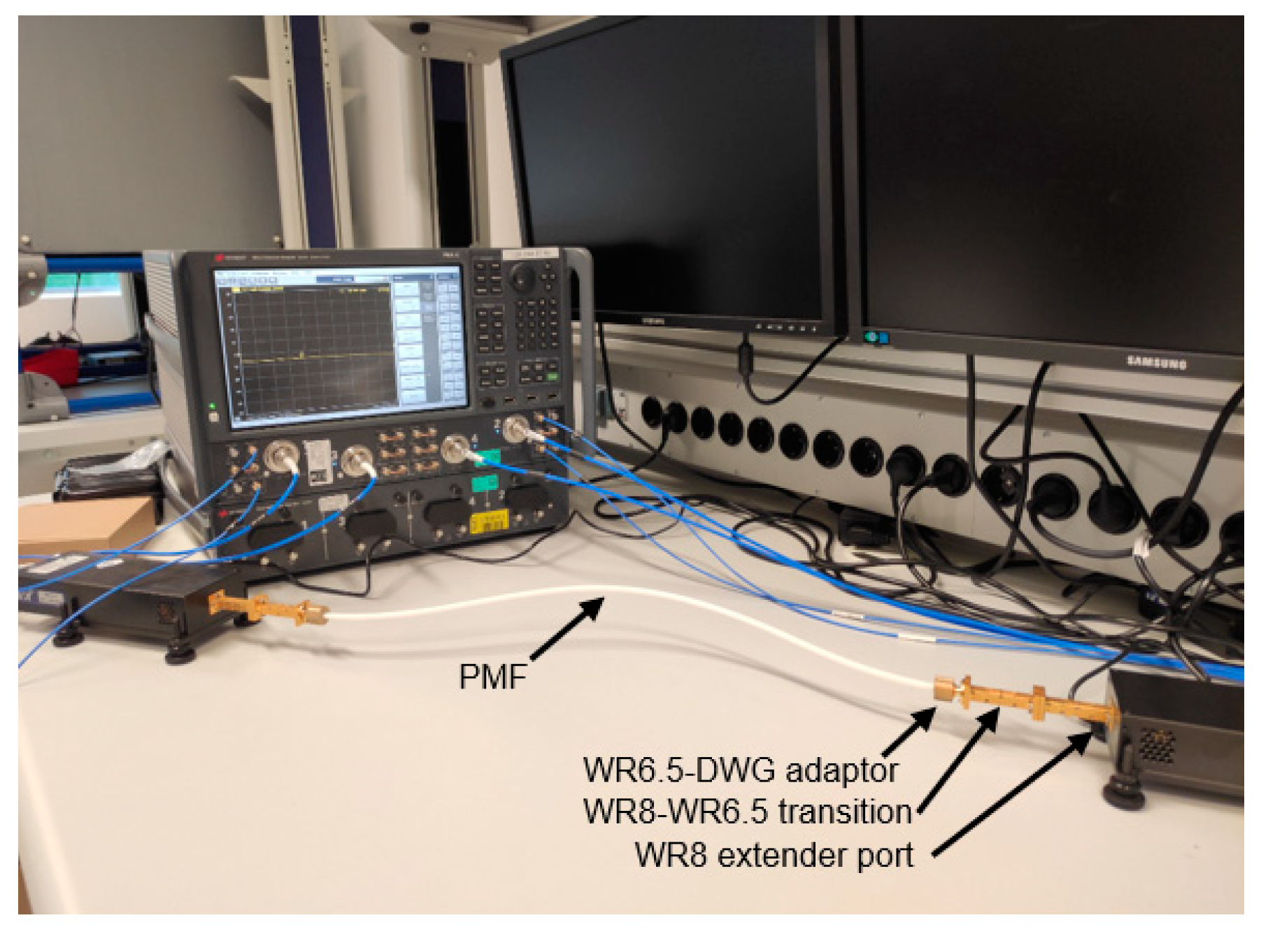
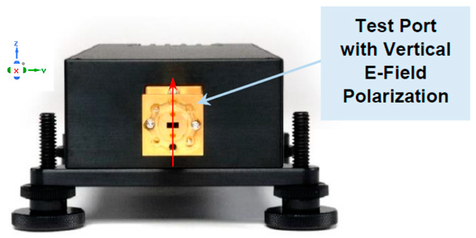
4.2. Coupler Measurement
5. Conclusions
Author Contributions
Funding
Institutional Review Board Statement
Informed Consent Statement
Data Availability Statement
Conflicts of Interest
References
- Mattia, O.E.; Sawaby, M.; Zheng, K.; Arbabian, A.; Murmann, B. A 10-Gbps Continuous-Time Linear Equalizer for mm-Wave Dielectric Waveguide Communication. IEEE Solid-State Circuit Lett. 2020, 3, 266–269. [Google Scholar] [CrossRef]
- Zhong, Q.; Chen, Z.; Sharma, N. 300-GHz CMOS QPSK Transmitter for 30-Gbps Dielectric Waveguide Communication. In Proceedings of the IEEE Custom Integrated Circuits Conference, San Diego, CA, USA, 8–11 April 2018. [Google Scholar]
- Momson, I.; Dong, S.; Yelleswarapu, P. 315-GHz Self-Synchronizing Minimum Shift Keying Receiver in 65-nm CMOS. In Proceedings of the IEEE Symposium on VLSI Circuits, Honolulu, HI, USA, 16–19 June 2020. [Google Scholar]
- Balanis, C.A. Advanced Engineering Electromagnetics; Wiley: Singapore, 2012. [Google Scholar]
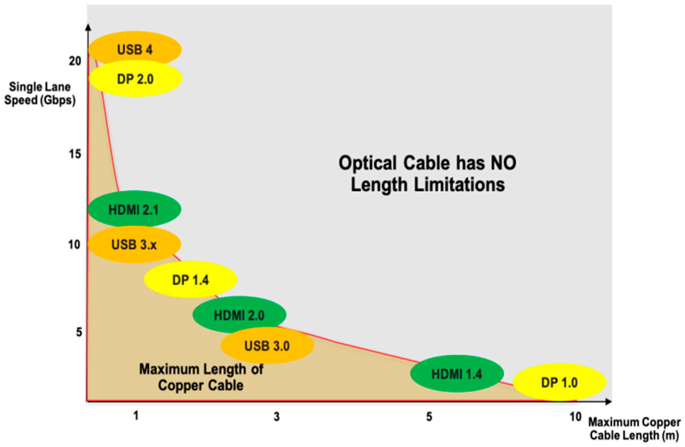
- Silicon Line GmbH. Available online: https://www.silicon-line.com/copper-cable-limitations/ (accessed on 1 February 2023).
- De Vit, M.; Ooms, S.; Zhang, Y.; Reynaert, P. Polymer Microwave Fibers. IEEE Microw. Mag. 2020, 21, 51–66. [Google Scholar]
- Dolatsha, N.; Chen, C.; Arbabian, A. Loss and Dispersion Limitations in mm-Wave Dielectric Waveguides for High-Speed Links. IEEE Trans. Terahertz Sci. Technol. 2016, 6, 637–640. [Google Scholar] [CrossRef]
- Kim, Y.; Nan, L.; Cong, J.; Chang, M.-C. High-speed mm-wave datalink based on hollow plastic cable and cmos transceiver. IEEE Microw. Wirel. Compon. Lett. 2013, 23, 674–676. [Google Scholar] [CrossRef]
- Reynaert, P.; Tytgat, M.; Volkaerts, W.; Standaert, A.; Zhang, Y.; Wit, M.D. Polymer Microwave Fibers: A blend of RF copper and optical communication. In Proceedings of the European Solid-State Circuits Conference, Lausanne, Switzerland, 12–15 September 2016. [Google Scholar]
- Van Thienen, N.; Reynaert, P.; Zhang, Y.; De Wit, M. An 18 Gbps polymer microwave fiber (PMF) communication link in 40nm CMOS. In Proceedings of the European Solid-State Circuit Conference, Lausanne, Switzerland, 12–15 September 2016. [Google Scholar]
- Thienen, N.; Reynaert, P. A 120GHz In-Band Full-Duplex PMF Transceiver with Tunable Electrical-Balance Duplexer in 40nm CMOS. In Proceedings of the IEEE European Solid State Circuits Conference, Leuven, Belgium, 11–14 September 2017. [Google Scholar]
- Dens, K.; Vaes, J.; Ooms, S.; Wagner, M.; Reynaert, P. A PAM4 Dielectric Waveguide Link in 28 nm CMOS. In Proceedings of the IEEE European Conference on Solid-State Circuits, Grenoble, France, 13–22 September 2021. [Google Scholar]
- Standaert, A.; Reynaert, P. Analysis of Hollow Circular Polymer Waveguides at Millimeter Wavelengths. IEEE Trans. Microw. Theory Tech. 2016, 64, 3068–3077. [Google Scholar] [CrossRef]
- De Wit, M.; Zhang, Y.; Reynaert, P. Analysis and Design of a Foam-Cladded PMF Link With Phase Tuning in 28-nm CMOS. IEEE J. Solid-State Circuits 2019, 54, 1960–1969. [Google Scholar] [CrossRef]
- Dolatsha, N.; Arbabian, A. Dielectric Waveguide with Planar Multi-Mode Excitation for High Data-Rate Chip-to-Chip Interconnects. In Proceedings of the IEEE International Conference on Ultra-Wideband, Sydney, Australia, 15–18 September 2013. [Google Scholar]
- Sawaby, M.; Dolatsha, N.; Grave, B.; Chen, C.; Arbabian, A. A Fully Packaged 130-GHz QPSK Transmitter With an Integrated PRBS Generator. IEEE Solid-State Circuit Lett. 2018, 1, 166–169. [Google Scholar] [CrossRef]
- Meyer, A.; Schneider, M. Signal distortions in circular dielectric waveguides at mm-wave frequencies. Int. J. Microw. Wirel. Technol. 2021, 14, 8–18. [Google Scholar] [CrossRef]
- Holloway, J.W.; Boglione, L.; Hancock, T.M.; Han, R. A Fully Integrated Broadband Sub-mmWave Chip-to-Chip Interconnect. IEEE Trans. Microw. Theory Tech. 2017, 65, 2373–2386. [Google Scholar] [CrossRef]
- Volkaerts, W.; Thienen, N.V.; Reynaert, P. 10.2 An FSK plastic waveguide communication link in 40nm CMOS. In Proceedings of the IEEE International Solid-State Circuits Conference, San Francisco, CA, USA, 22–26 February 2015. [Google Scholar]
- Rougier, B.; Aubert, H.; Lefrançois, A. Measurement of Shock Wave and Particle Velocities in Shocked Dielectric Material from Millimeter-Wave Remote Sensing. In Proceedings of the 2018 48th European Microwave Conference (EuMC), Madrid, Spain, 23–27 September 2018; pp. 855–858. [Google Scholar] [CrossRef]
- Lou, Z.; Jian-Ming, J. Modeling and Simulation of Broad-Band Antennas Using the Time-Domain Finite Element Method. IEEE Trans. Antennas Propag. 2005, 53, 4099–4110. [Google Scholar]
- Bao, H.; Nielsen, K.; Bang, O.; Jepsen, P.U. Dielectric tube waveguides with absorptive cladding for broadband, low-dispersion and low loss THz guiding. Sci. Rep. 2015, 5, 7620. [Google Scholar] [CrossRef]
- Krishnamoorthy, A.V.; Goossen, K.W.; Jan, W.; Zheng, X.; Ho, R.; Li, G.; Rozier, R.; Liu, F.; Patil, D.; Lexau, J.; et al. Progress in Low-Power Switched Optical Interconnects. IEEE J. Sel. Top. Quantum Electron. 2011, 17, 357–376. [Google Scholar] [CrossRef]
- Oliver, G. Low-Loss Materials in High Frequency Electronics and the Challenges of Measurement; DuPont: Wilmington, DE, USA, 2015. [Google Scholar]
- Yeh, C.; Shimabukuro, F.I. The Essence of Dielectric Waveguides; Springer: Berlin/Heidelberg, Germany, 2008. [Google Scholar]
- Stratton, J.A. Electromagnetic Theory; McGraw-Hill Book Company: New York, NY, USA, 1941. [Google Scholar]
- Marcatili, E.A.J. Dielectric Rectangular Waveguide and Directional Coupler for Integrated Optics. Bell Syst. Tech. J. 1969, 48, 2071–2102. [Google Scholar] [CrossRef]
- Huynh, N.H.; Saverio, T.; Wojnowski, M.; Haubner, G.; Pahlke, S.; Schmitt, J.; Mayr, H.; Würtele, J.; Rueddenklau, U.; Nasr, I.; et al. eWLB package for millimeter wave application. In Proceedings of the 2015 European Microelectronics Packaging Conference (EMPC), Friedrichshafen, Germany, 14–16 September 2015; pp. 1–5. [Google Scholar]
- Schmidbauer, P.; Wojnowski, M.; Weigel, R.; Hagelauer, A. Wafer Level Package Integrated Antenna Concepts for Circular Polarization. In Proceedings of the 2018 IEEE 27th Conference on Electrical Performance of Electronic Packaging and Systems (EPEPS), San Jose, CA, USA, 14–17 October 2018. [Google Scholar]
- Wojnowski, M.; Lachner, R.; Bock, J.; Wagner, C.; Starzer, F.; Sommer, G.; Pressel, K.; Weigel, R. Embedded wafer level ball grid array (eWLB) technology for millimeter-wave applications. In Proceedings of the 2011 IEEE 13th Electronics Packaging Technology Conference, Singapore, 7–9 December 2011; pp. 423–429. [Google Scholar] [CrossRef]
- Hassona, A.; Vassilev, V.; He, Z.S.; Mariotti, C.; Dielacher, F.; Zirath, H. Silicon taper-based D-band chip to waveguide interconnect for millimeter-wave systems. IEEE Microw. Compon. Lett. 2017, 27, 1092–1094. [Google Scholar] [CrossRef]


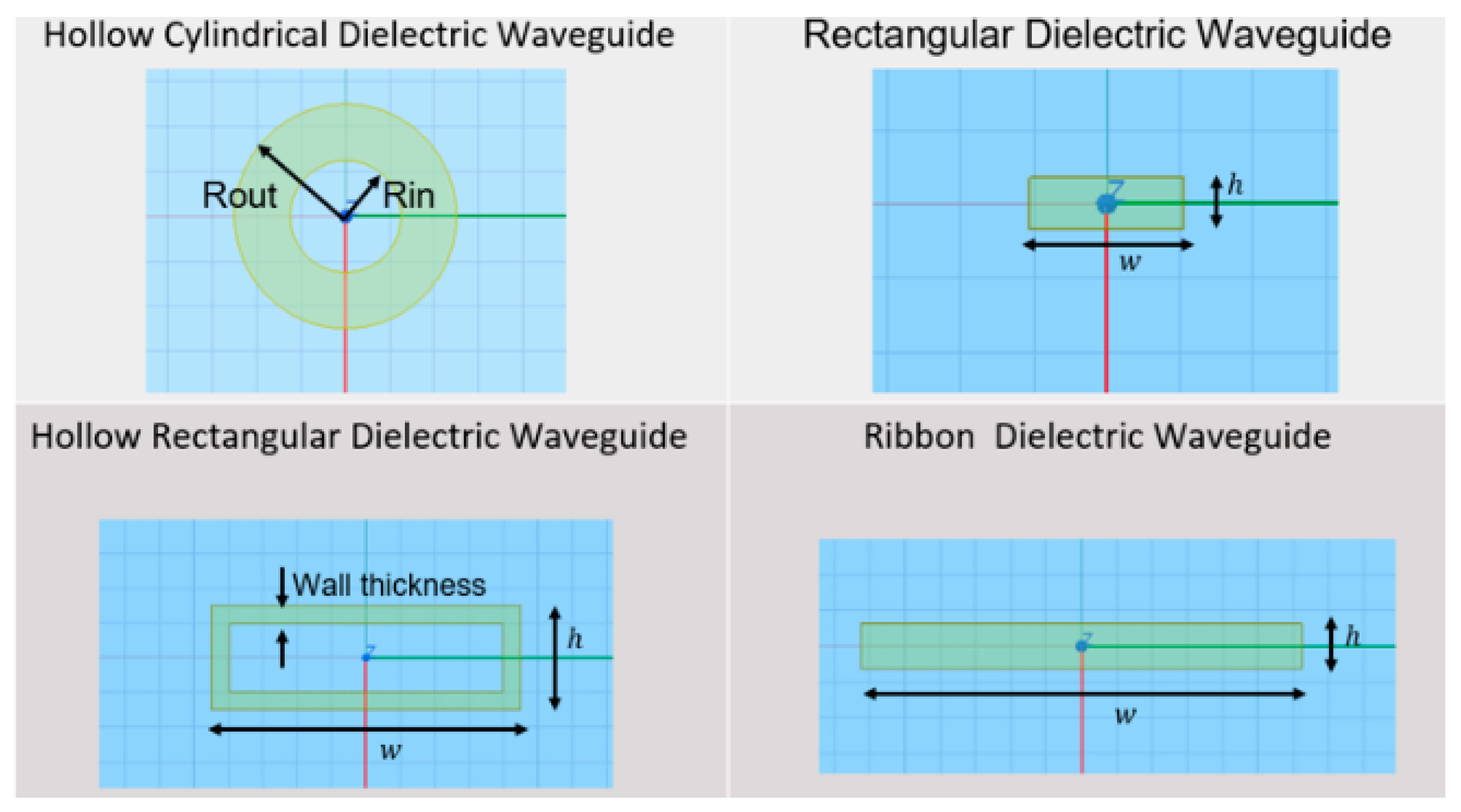
| PMF Structure | Dimensions |
|---|---|
| Hollow-core cylindrical PMF | Rin = 0.5 mm Rout = 1 mm |
| Hollow-core rectangular PMF | h = 0.6 mm w = 2.4 mm wall thickness = 150 μm |
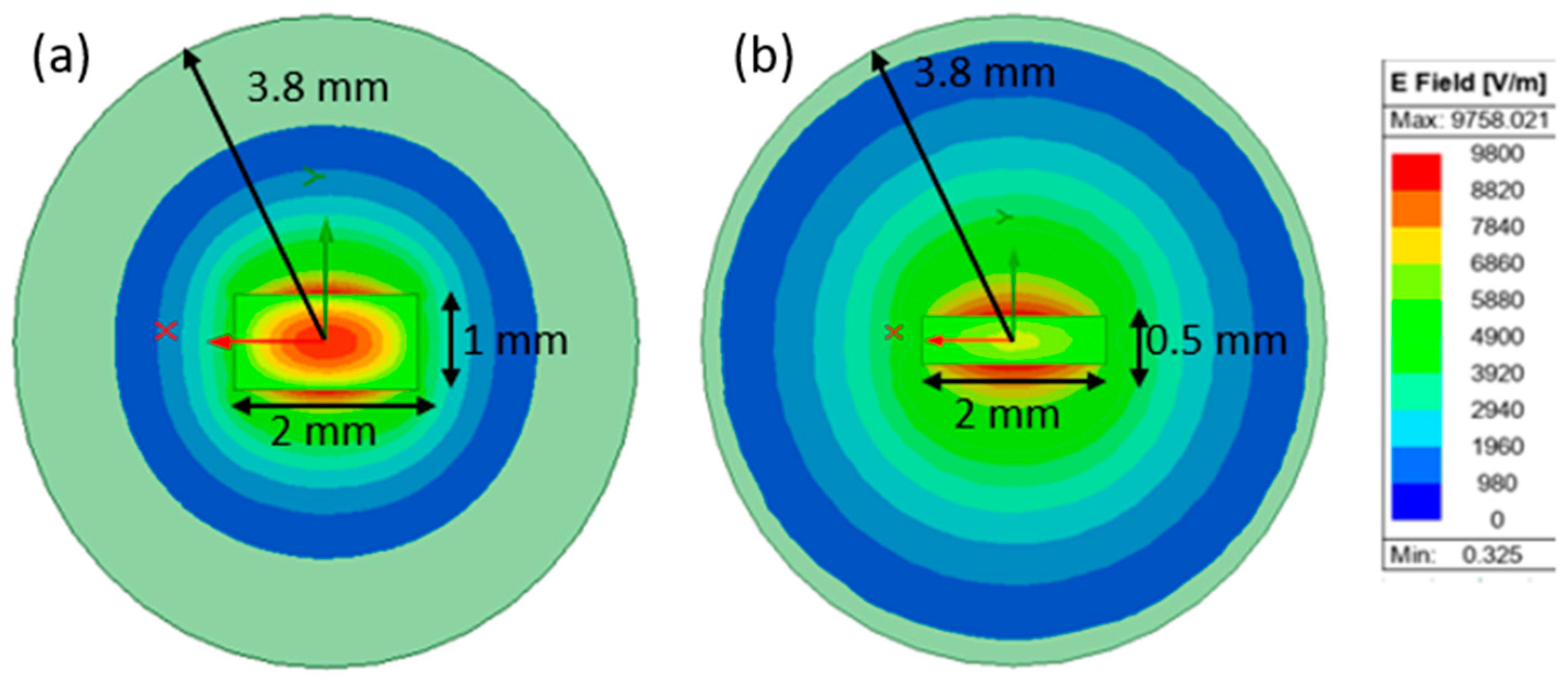
| Solid-core rectangular PMF | h = 0.5 mm w = 2 mm |
| Ribbon PMF | w = 3.2 mm h = 0.32 mm |
| Ref. | Coupling Type | Frequency (GHz) | Implementation | Coupling Loss (dB) |
|---|---|---|---|---|
| [8] | Wireless | 60 | On-Chip Antenna | 6 (simulated) |
| [9] | Wireless | 120 | On-Chip Antenna | 11 (measured) |
| [11] | Wireless | 120 | On-Chip Antenna | 7.1 (simulated) |
| [10] | MMIC interface | 120 | PCB | 3.4 (measured) |
| [12] | Wireless | 140 | PCB | 3.5 (measured) |
| [16] | Wireless | 130 | Antenna-In-Package | 3 (measured) |
| This work | Wireless | 140 | Antenna-In-Package | 3.5 (measured) |
Disclaimer/Publisher’s Note: The statements, opinions and data contained in all publications are solely those of the individual author(s) and contributor(s) and not of MDPI and/or the editor(s). MDPI and/or the editor(s) disclaim responsibility for any injury to people or property resulting from any ideas, methods, instructions or products referred to in the content. |
© 2025 by the authors. Licensee MDPI, Basel, Switzerland. This article is an open access article distributed under the terms and conditions of the Creative Commons Attribution (CC BY) license (https://creativecommons.org/licenses/by/4.0/).
Share and Cite
Liakonis, V.; Papananos, Y.; Dielacher, F.; Wojnowski, M.; Hartner, W. Efficient Implementation of Polymer Microwave Fiber Links Employing Non-Galvanic Coupling Mechanism. Appl. Sci. 2025, 15, 1824. https://doi.org/10.3390/app15041824
Liakonis V, Papananos Y, Dielacher F, Wojnowski M, Hartner W. Efficient Implementation of Polymer Microwave Fiber Links Employing Non-Galvanic Coupling Mechanism. Applied Sciences. 2025; 15(4):1824. https://doi.org/10.3390/app15041824
Chicago/Turabian StyleLiakonis, Vasileios, Yannis Papananos, Franz Dielacher, Maciej Wojnowski, and Walter Hartner. 2025. "Efficient Implementation of Polymer Microwave Fiber Links Employing Non-Galvanic Coupling Mechanism" Applied Sciences 15, no. 4: 1824. https://doi.org/10.3390/app15041824
APA StyleLiakonis, V., Papananos, Y., Dielacher, F., Wojnowski, M., & Hartner, W. (2025). Efficient Implementation of Polymer Microwave Fiber Links Employing Non-Galvanic Coupling Mechanism. Applied Sciences, 15(4), 1824. https://doi.org/10.3390/app15041824