
Design of Shadow Filter Using Low-Voltage Multiple-Input Operational Transconductance Amplifiers


Abstract
1. Introduction
2. Proposed Circuit
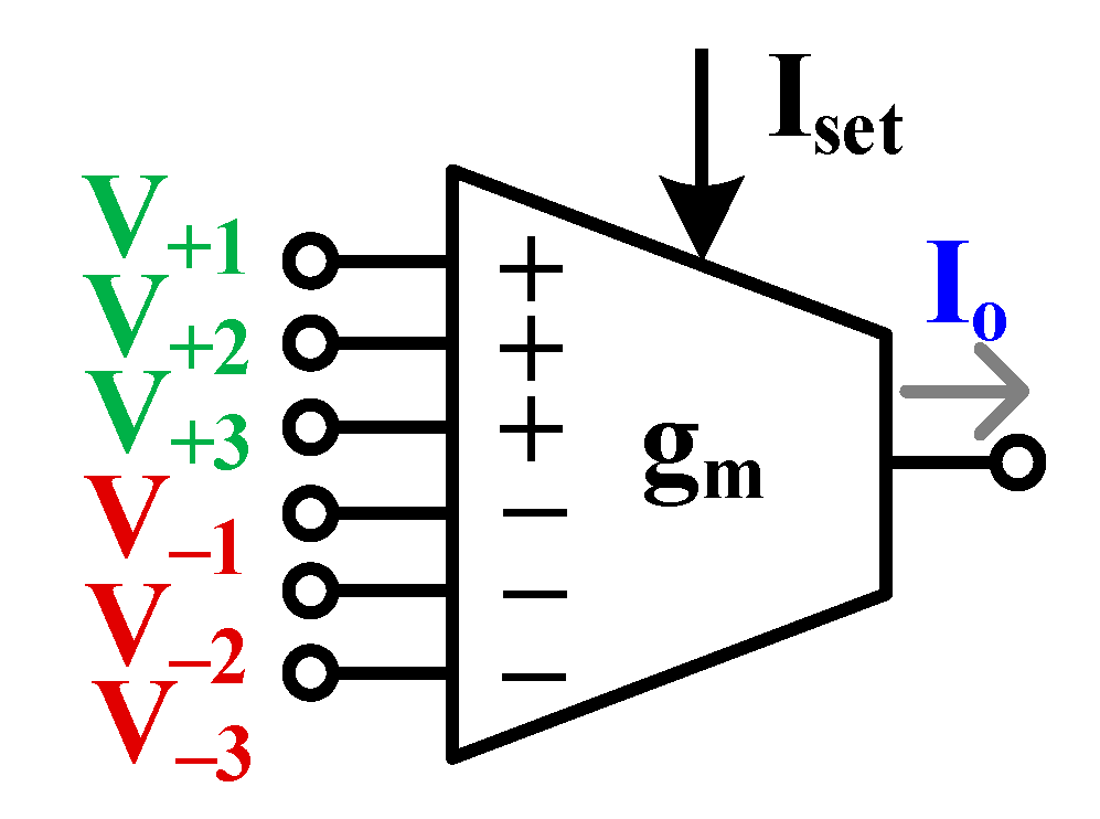
2.1. MI-OTA
- at the operating point;
- is the subthreshold slope factor for p-channel transistors;
- is the thermal potential;
- = (W3,4/L3,4)/(W1,2/L1,2) is the relative aspect ratio of the two matched transistor pairs M3,4 − M1,2;
- is the AC voltage gain of the input capacitive divider.
- The input capacitive divider (), which attenuates the input signal.
- The control of transistors M1 and M2 through their bulk terminals, in which the bulk transconductance is inherently of the gate transconductance.
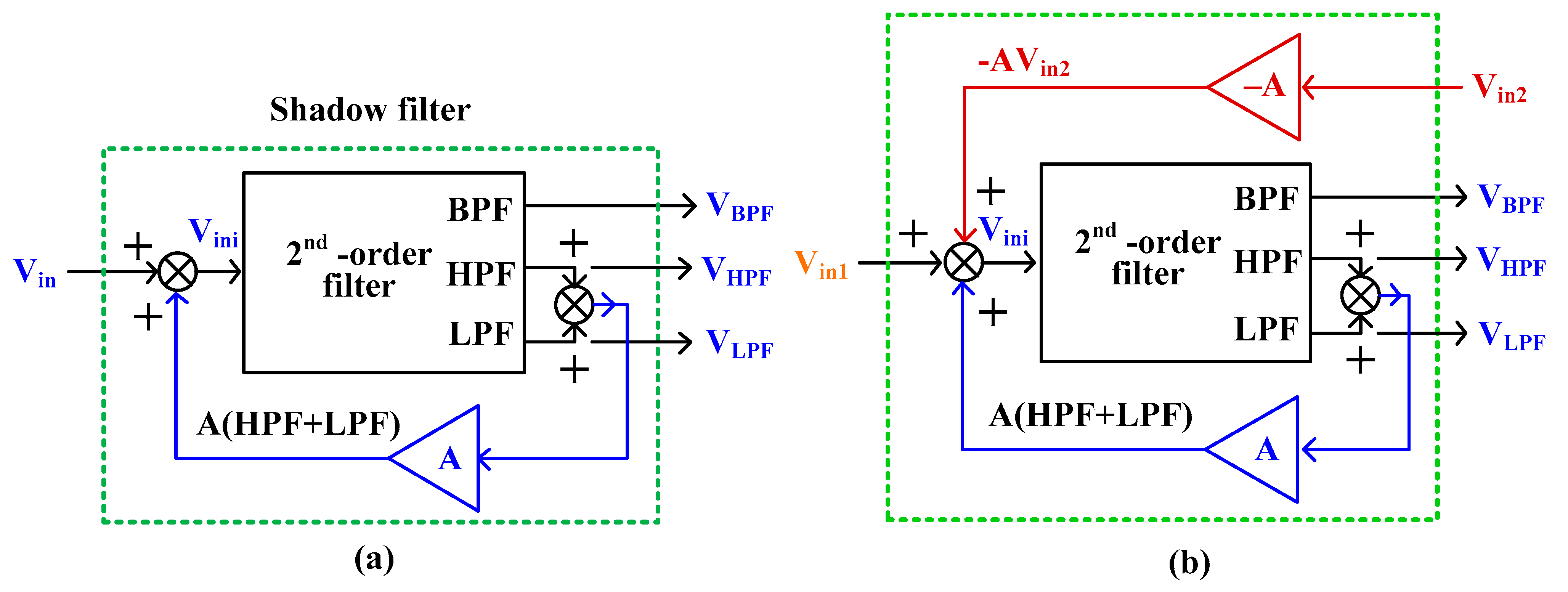
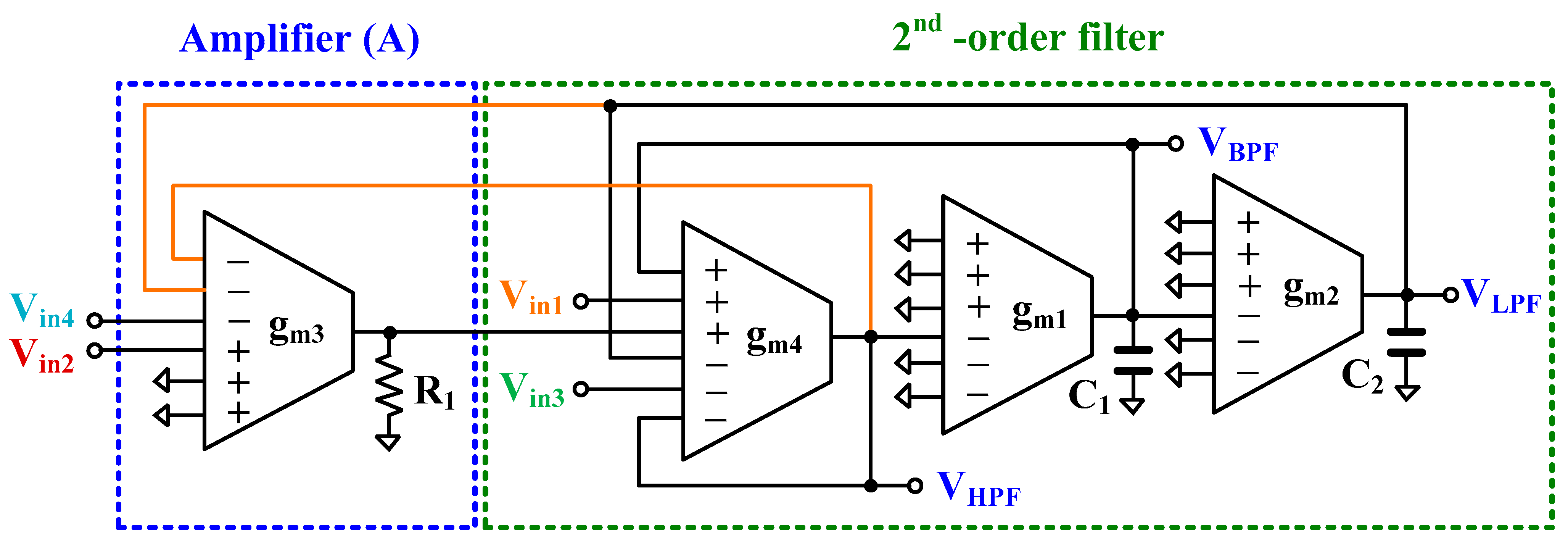
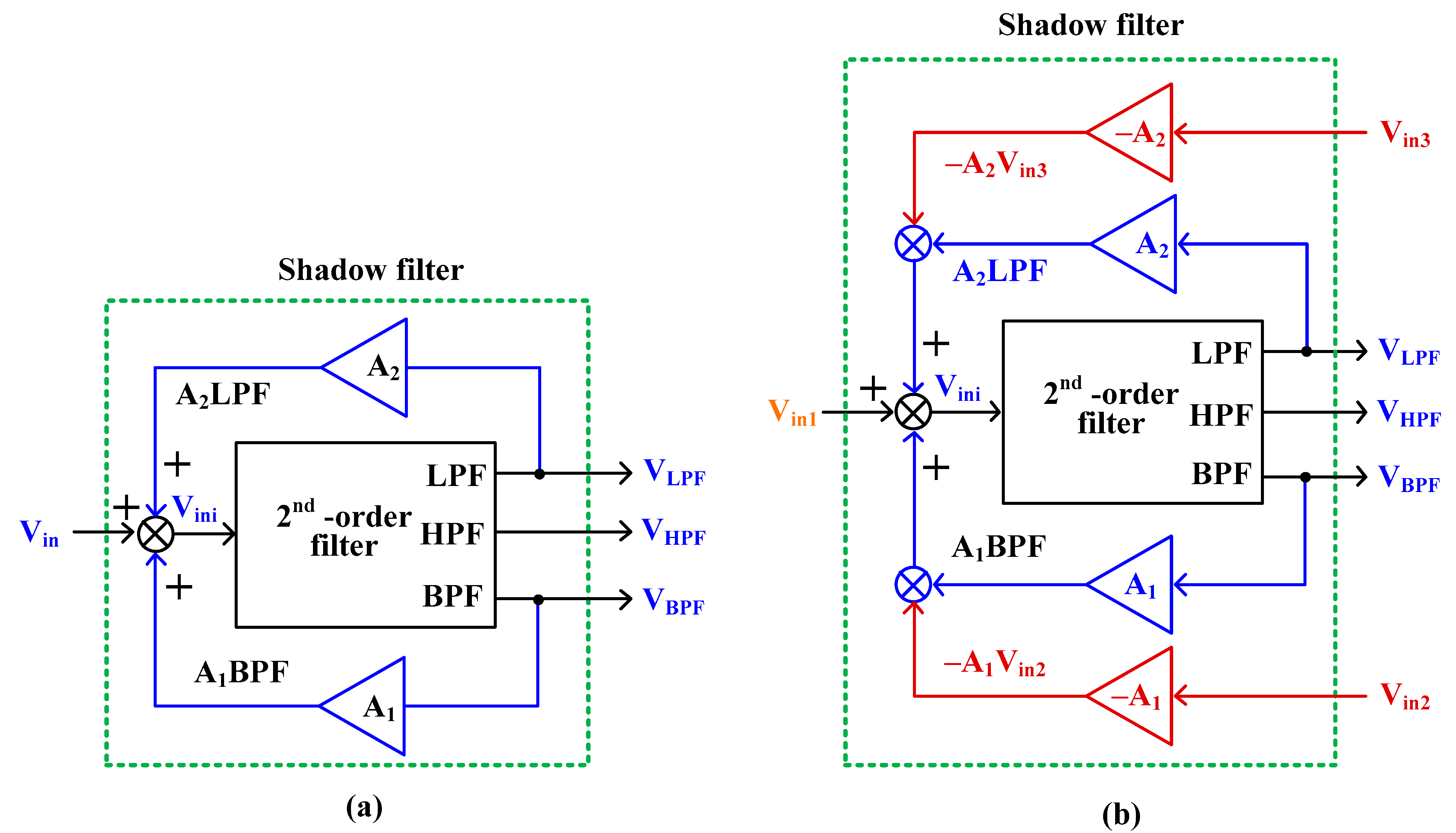
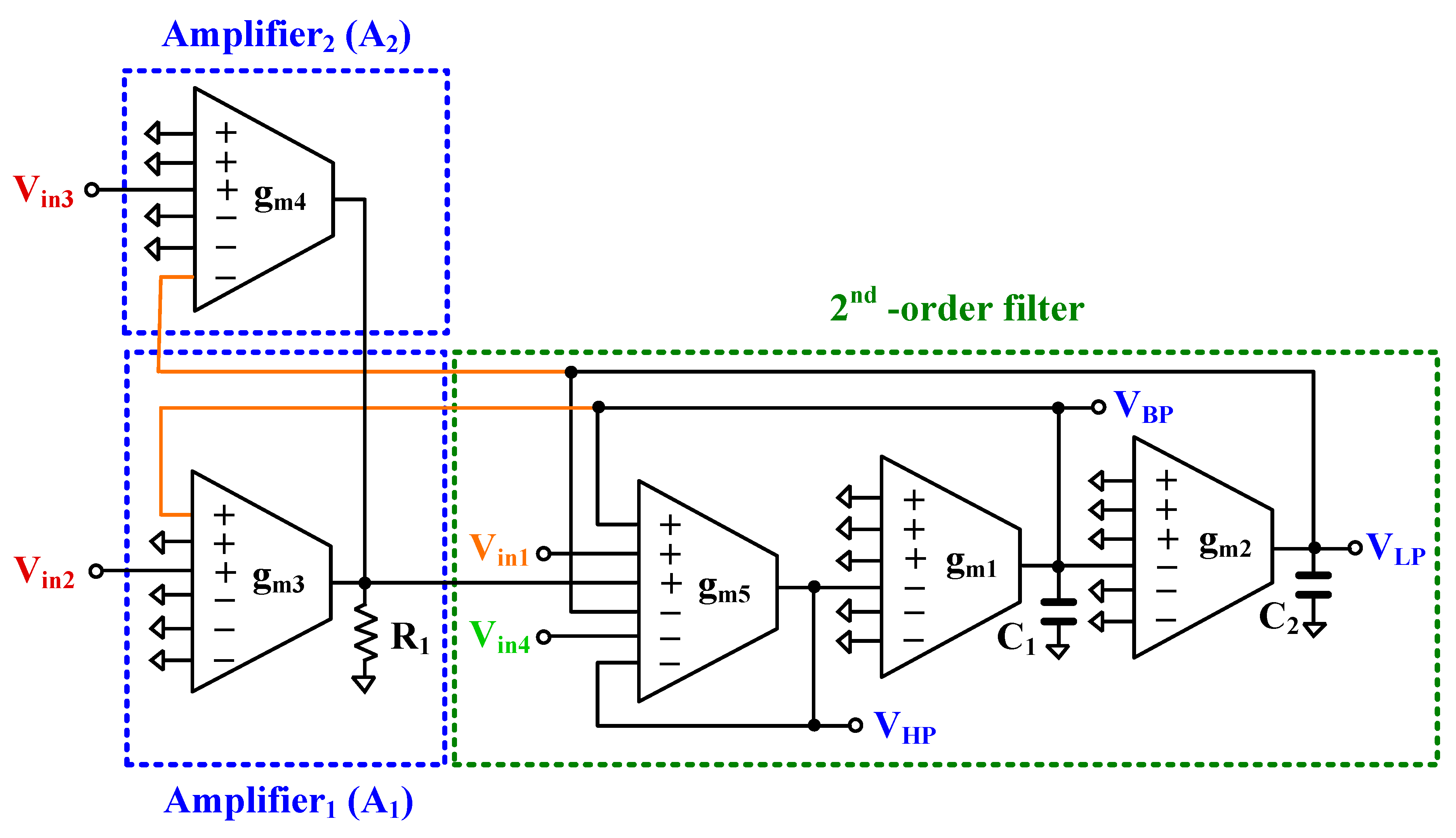
2.2. Proposed First Shadow Filters
2.3. Proposed Second Shadow Filters
2.4. Non-Ideal Analysis
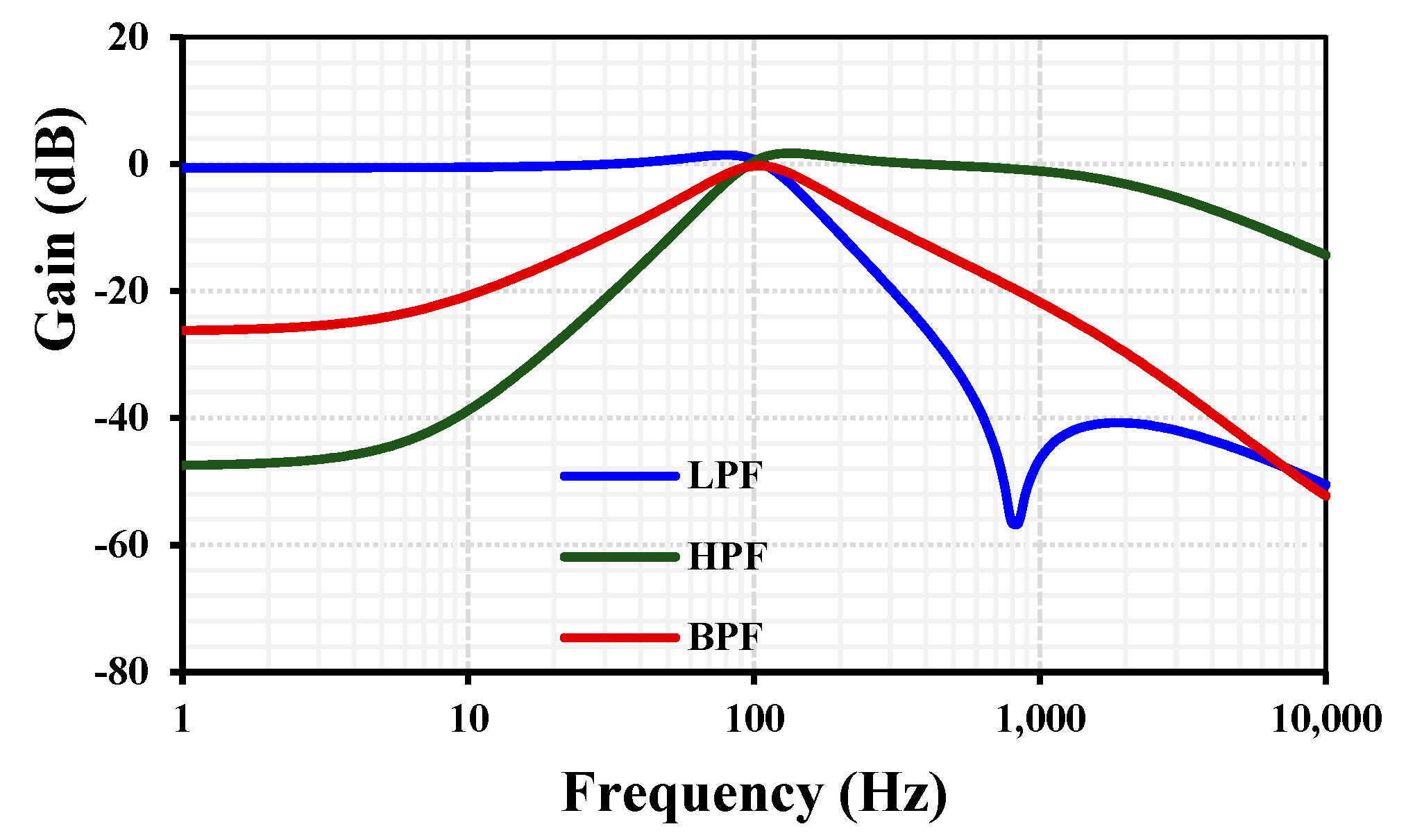
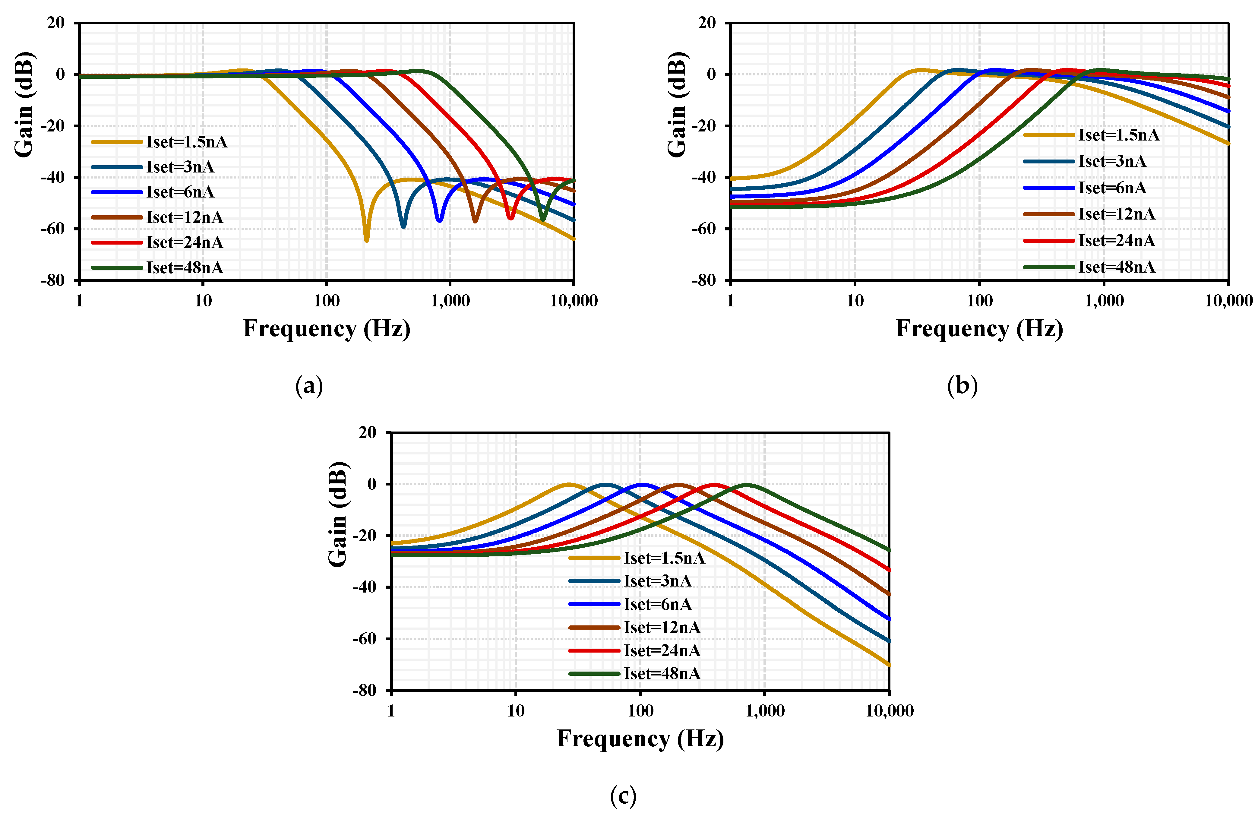
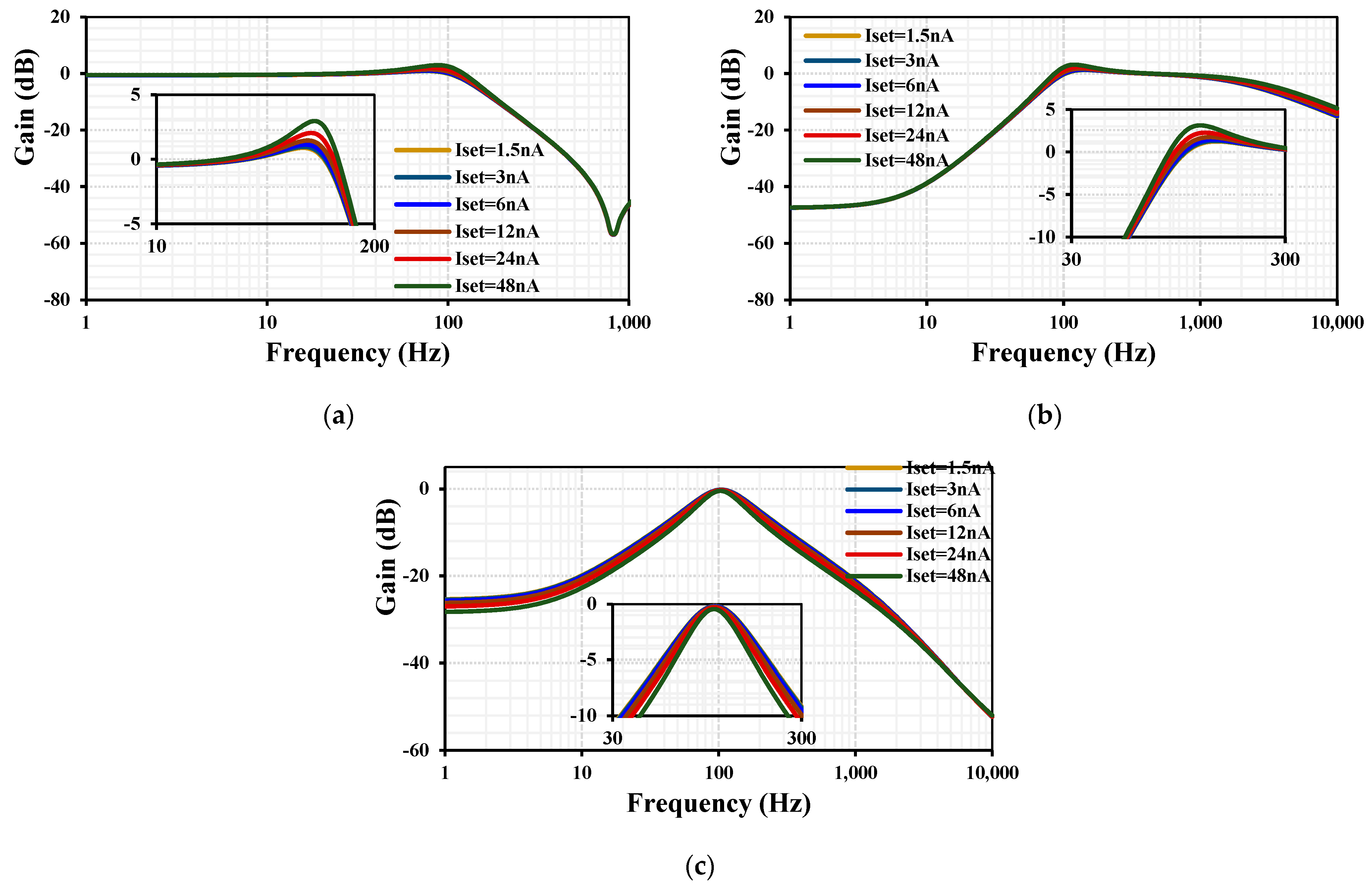
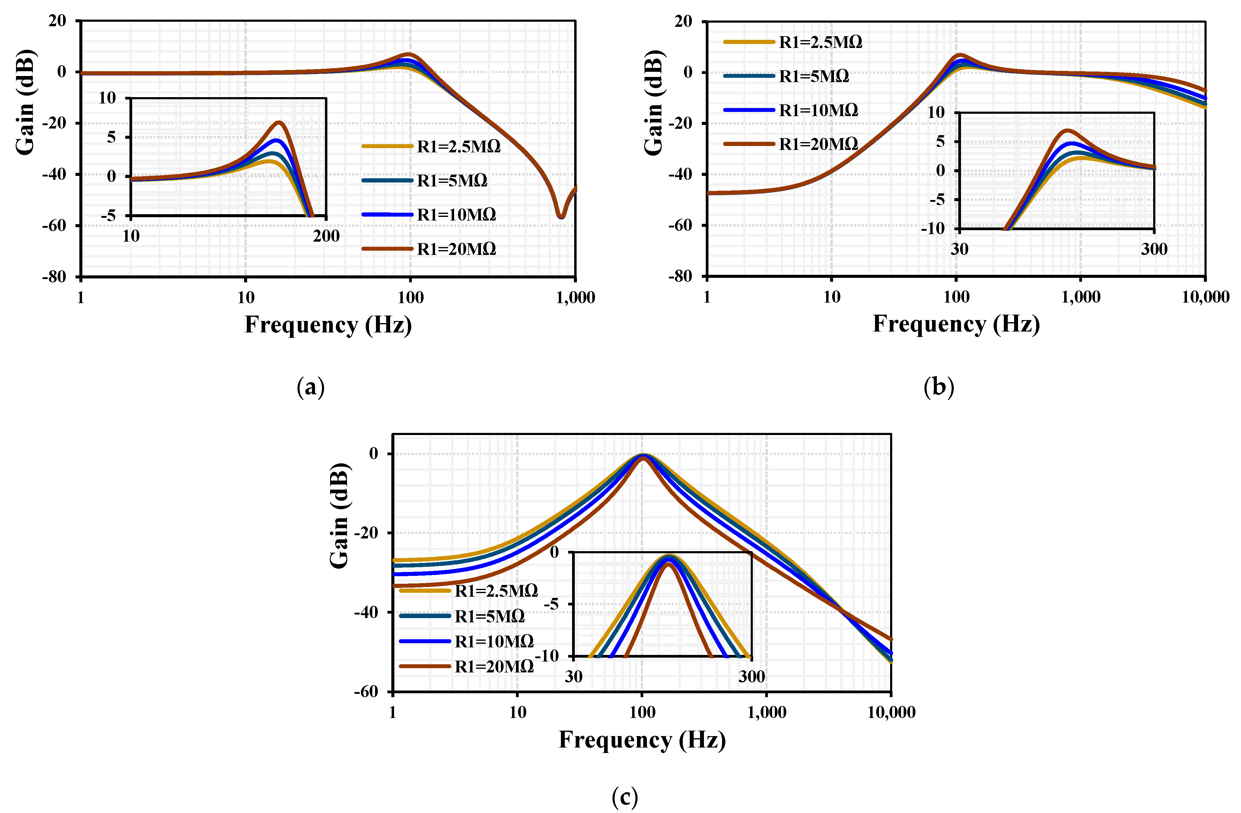
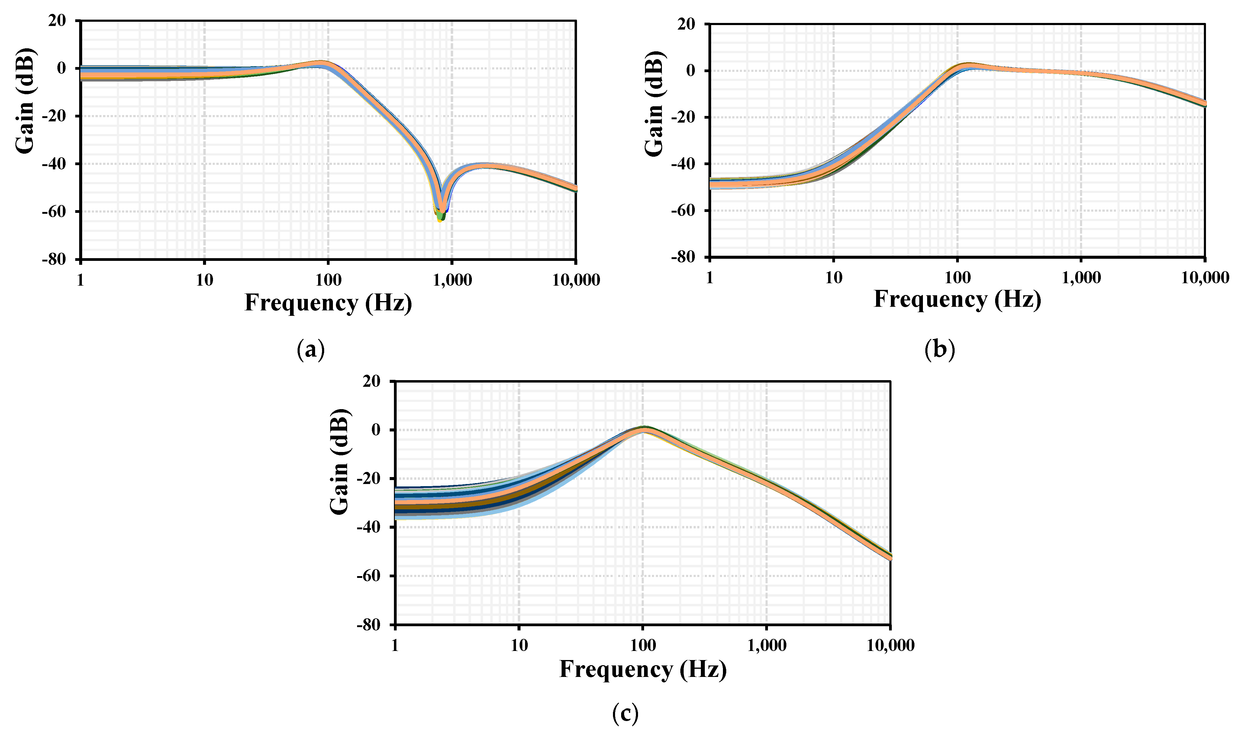
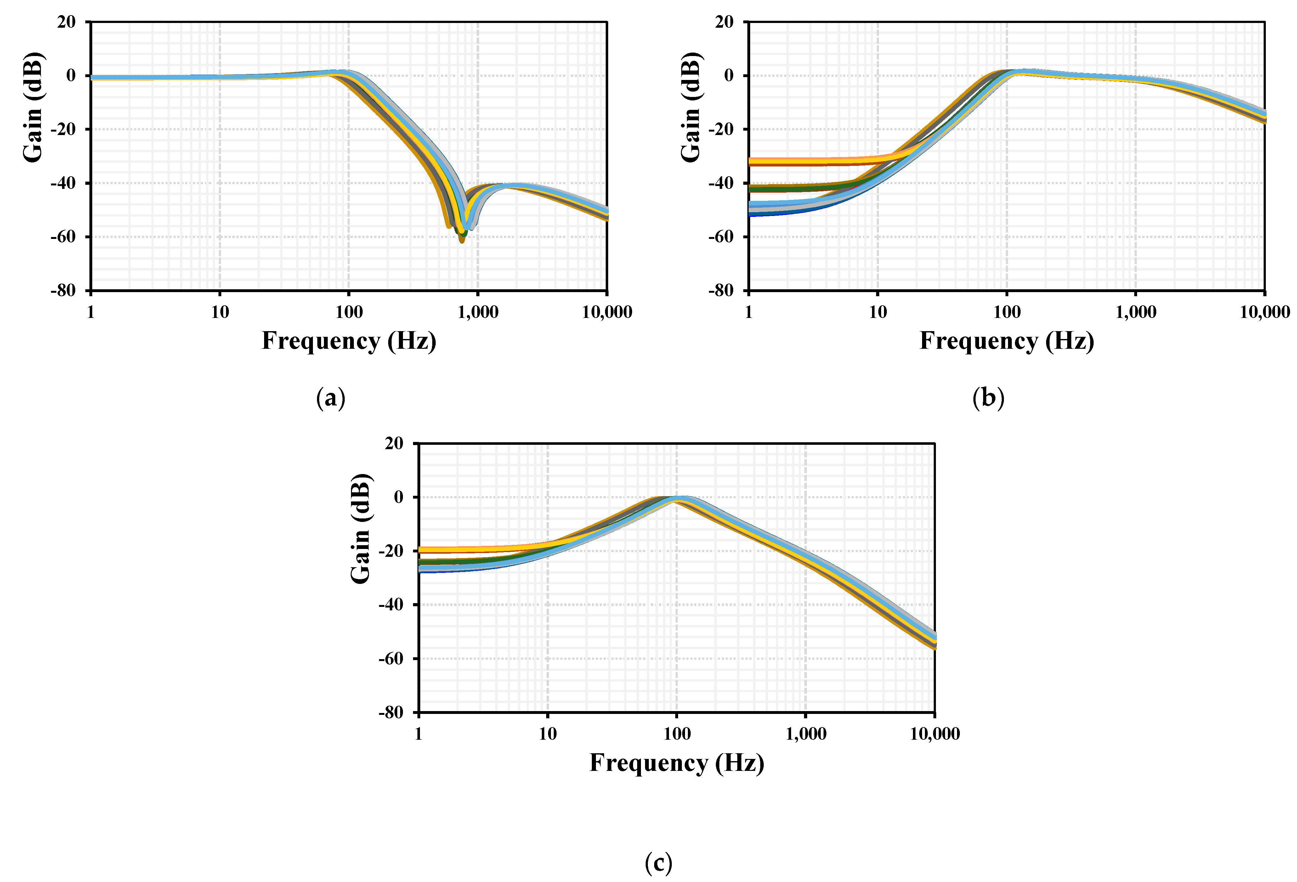
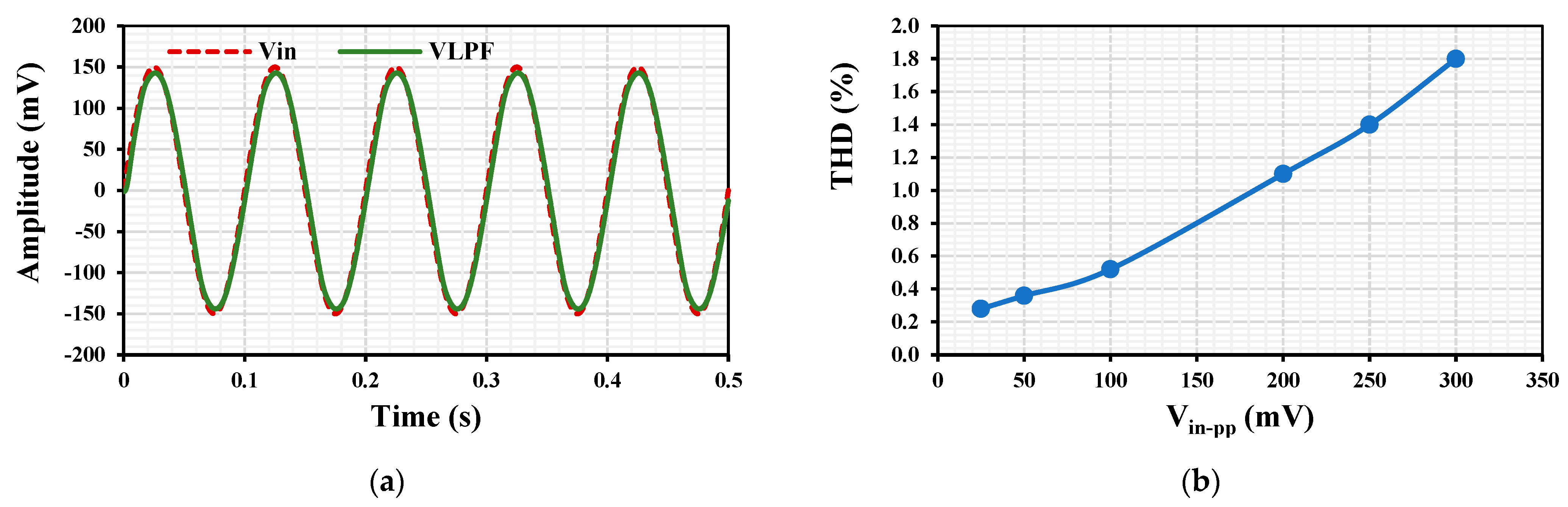
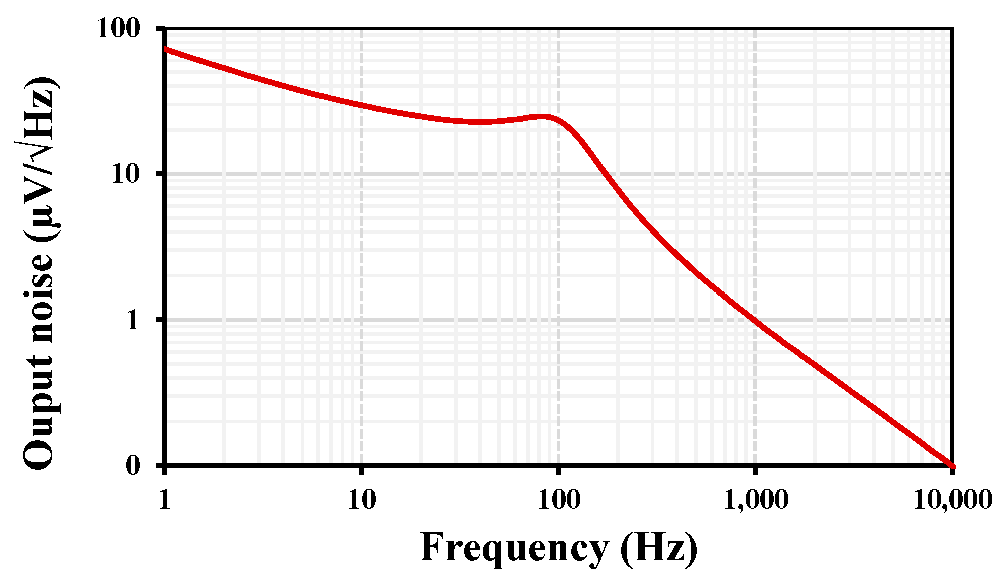
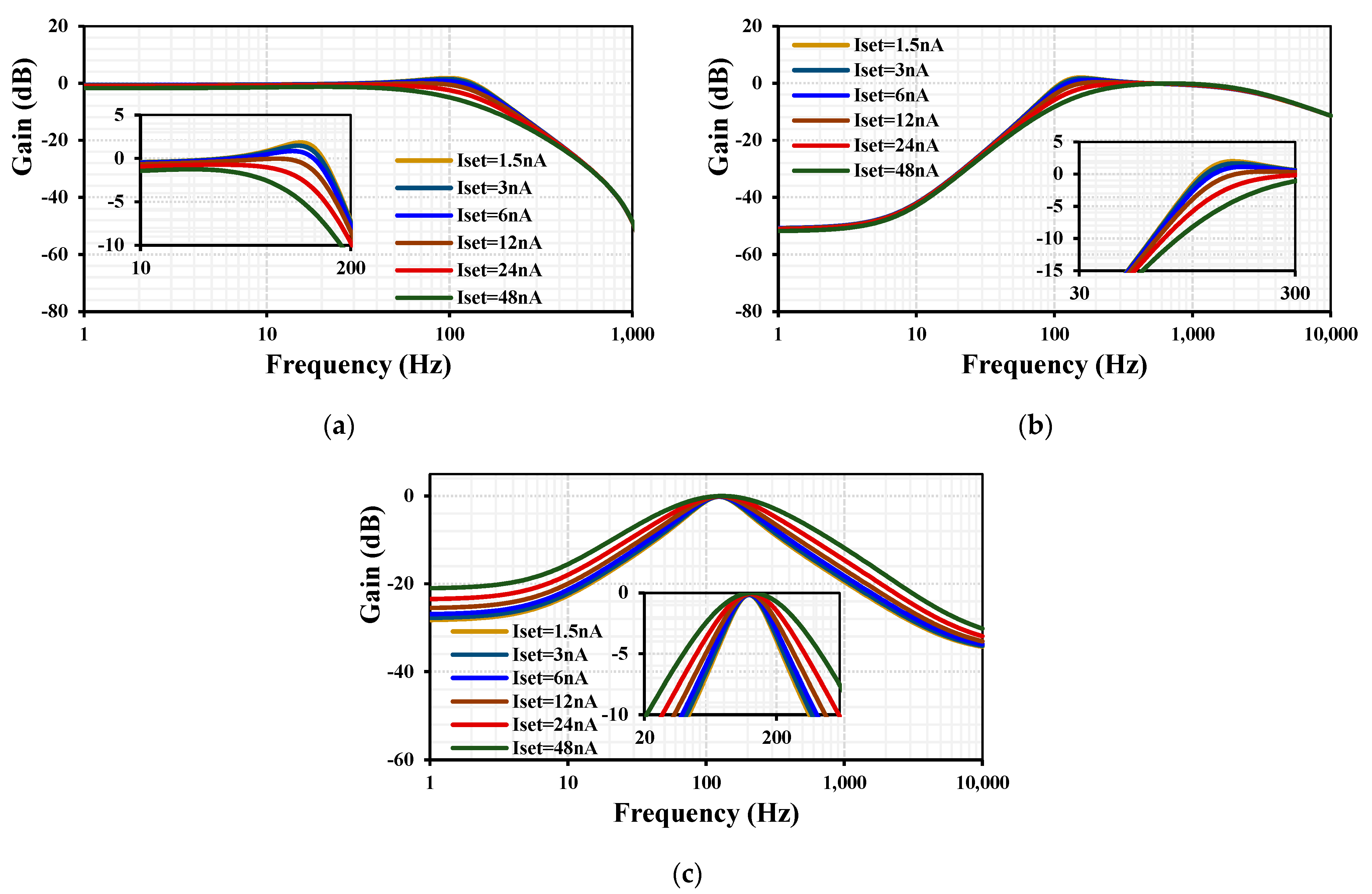
3. Simulation Results
4. Conclusions
Author Contributions
Funding
Institutional Review Board Statement
Informed Consent Statement
Data Availability Statement
Conflicts of Interest
References
- Wang, C.; Liu, H.; Zhao, Y. A New Current-Mode Current-Controlled Universal Filter Based on CCCII(±). Circuits Syst. Signal Process. 2008, 27, 673–682. [Google Scholar] [CrossRef]
- Hassan, T.M.; Mahmoud, S.A. Fully Programmable Universal Filter with Independent Gain-ωo-Q Control Based on New Digitally Programmable CMOS CCII. J. Circuits Syst. Comput. 2009, 18, 875–897. [Google Scholar] [CrossRef]
- Prommee, P.; Pattanatadapong, T. Realization of Tunable Pole-Q Current-Mode OTA-C Universal Filter. Circuits Syst. Signal Process. 2010, 29, 913–924. [Google Scholar] [CrossRef]
- Jaikla, W.; Khateb, F.; Kulej, T.; Pitaksuttayaprot, K. Universal Filter Based on Compact CMOS Structure of VDDDA. Sensors 2021, 21, 1683. [Google Scholar] [CrossRef]
- Kumngern, M.; Khateb, F.; Kulej, T.; Knobnob, B. 1 V Tunable High-Quality Universal Filter Using Multiple-Input Operational Transconductance Amplifiers. Sensors 2024, 24, 3013. [Google Scholar] [CrossRef]
- Lakys, Y.; Fabre, A. Shadow Filters: New Family of Second-Order Filters. Electron. Lett. 2010, 46, 276–277. [Google Scholar] [CrossRef]
- Biolkova, V.; Biolek, D. Shadow Filters for Orthogonal Modification of Characteristic Frequency and Bandwidth. Electron. Lett. 2010, 46, 830–831. [Google Scholar] [CrossRef]
- Khateb, F.; Jaikla, W.; Kulej, T.; Kumngern, M.; Kubánek, D. Kubanek. Shadow Filters Based on DDCC. IET Circuits Devices Syst. 2017, 11, 631–637. [Google Scholar] [CrossRef]
- Abuelma’Atti, M.T.; Almutairi, N. New CFOA-Based Shadow Banpass Filter. In Proceedings of the 2016 International Conference on Electronics, Information, and Communications (ICEIC), Danang, Vietnam, 27–30 January 2016; pp. 1–3. [Google Scholar] [CrossRef]
- Abuelma’atti, M.T.; Almutairi, N.R. Almutairi. New Current-Feedback Operational-Amplifier Based Shadow Filters. Analog. Integr. Circuits Signal Process. 2016, 86, 471–480. [Google Scholar] [CrossRef]
- Nako, J.; Psychalinos, C.; Minaei, S. First-Order Universal Shadow Filter Designs with Scaled Time Constants. Int. J. Circuit Theory Appl. 2024, 52, 4040–4053. [Google Scholar] [CrossRef]
- Anurag, R.; Pandey, R.; Pandey, N.; Singh, M.; Jain, M. OTRA Based Shadow Filters. In Proceedings of the 2015 Annual IEEE India Conference (INDICON), New Delhi, India, 17–20 December 2015; pp. 1–4. [Google Scholar] [CrossRef]
- Nand, D.; Pandey, N. New Configuration for OFCC-Based CM SIMO Filter and Its Application as Shadow Filter. Arab. J. Sci. Eng. 2018, 43, 3011–3022. [Google Scholar] [CrossRef]
- Buakaew, S.; Narksarp, W.; Wongtaychatham, C. Fully Active and Minimal Shadow Bandpass Filter. In Proceedings of the 2018 International Conference on Engineering, Applied Sciences, and Technology (ICEAST), Phuket, Thailand, 4–7 July 2018; pp. 1–4. [Google Scholar] [CrossRef]
- Buakaew, S.; Narksarp, W.; Wongtaychatham, C. Shadow Bandpass Filter with Q-Improvement. In Proceedings of the 2019 5th International Conference on Engineering, Applied Sciences and Technology (ICEAST), Luang Prabang, Laos, 2–5 July 2019; pp. 1–4. [Google Scholar] [CrossRef]
- Buakaew, S.; Narksarp, W.; Wongtaychatham, C. High Quality-Factor Shadow Bandpass Filters with Orthogonality to the Characteristic Frequency. In Proceedings of the 2020 17th International Conference on Electrical Engineering/Electronics, Computer, Telecommunications and Information Technology (ECTI-CON), Phuket, Thailand, 24–27 June 2020; pp. 372–375. [Google Scholar] [CrossRef]
- Buakaew, S.; Wongtaychatham, C. Boosting the Quality Factor of the Shadow Bandpass Filter. J. Circuits Syst. Comput. 2022, 31, 2250248. [Google Scholar] [CrossRef]
- Moonmuang, P.; Pukkalanun, T.; Tangsrirat, W. Voltage Differencing Gain Amplifier-Based Shadow Filter: A Comparison Study. In Proceedings of the 2020 6th International Conference on Engineering, Applied Sciences and Technology (ICEAST), Chiang Mai, Thailand, 1–4 July 2020; pp. 1–4. [Google Scholar] [CrossRef]
- Varshney, G.; Pandey, N.; Pandey, R. Generalization of Shadow Filters in Fractional Domain. Int. J. Circuit Theory Appl. 2021, 49, 3248–3265. [Google Scholar] [CrossRef]
- Pandey, N.; Pandey, R.; Choudhary, R.; Sayal, A.; Tripathi, M. Realization of CDTA Based Frequency Agile Filter. In Proceedings of the 2013 IEEE International Conference on Signal Processing, Computing and Control (ISPCC), Solan, India, 26–28 September 2013; pp. 1–6. [Google Scholar] [CrossRef]
- Pandey, N.; Sayal, A.; Choudhary, R.; Pandey, R. Design of CDTA and VDTA Based Frequency Agile Filters. Adv. Electron. 2014, 2014, 176243. [Google Scholar] [CrossRef]
- Atasoyu, M.; Kuntman, H.; Metin, B.; Herencsar, N.; Cicekoglu, O. Design of Current-Mode Class 1 Frequency-Agile Filter Employing CDTAs. In Proceedings of the 2015 European Conference on Circuit Theory and Design (ECCTD), Trondheim, Norway, 24–26 August 2015; pp. 1–4. [Google Scholar] [CrossRef]
- Alaybeyoğlu, E.; Kuntman, H. A New Frequency Agile Filter Structure Employing CDTA for Positioning Systems and Secure Communications. Analog. Integr. Circuits Signal Process. 2016, 89, 693–703. [Google Scholar] [CrossRef]
- Chhabra, K.; Singhal, S.; Pandey, N. Realisation of CBTA Based Current Mode Frequency Agile Filter. In Proceedings of the 2019 6th International Conference on Signal Processing and Integrated Networks (SPIN), Noida, India, 7–8 March 2019; pp. 1076–1081. [Google Scholar] [CrossRef]
- Kumngern, M.; Khateb, F.; Kulej, T. Shadow Filters Using Multiple-Input Differential Difference Transconductance Amplifiers. Sensors 2023, 23, 1526. [Google Scholar] [CrossRef]
- Khateb, F.; Kumngern, M.; Kulej, T.; Ranjan, R.K. Ranjan. 0.5 V Multiple-Input Multiple-Output Differential Difference Transconductance Amplifier and Its Applications to Shadow Filter and Oscillator. IEEE Access 2023, 11, 31212–31227. [Google Scholar] [CrossRef]
- Huaihongthong, P.; Chaichana, A.; Suwanjan, P.; Siripongdee, S.; Sunthonkanokpong, W.; Supavarasuwat, P.; Jaikla, W.; Khateb, F. Single-Input Multiple-Output Voltage-Mode Shadow Filter Based on VDDDAs. AEU-Int. J. Electron. Commun. 2019, 103, 13–23. [Google Scholar] [CrossRef]
- Singh, D.; Paul, S.K. Realization of Current Mode Universal Shadow Filter. AEU-Int. J. Electron. Commun. 2020, 117, 153088. [Google Scholar] [CrossRef]
- Singh, D.; Paul, S.K. Mixed-Mode Universal Filter Using FD-CCCTA and Its Extension as Shadow Filter. Inf. MIDEM 2022, 52, 239–262. [Google Scholar] [CrossRef]
- Singh, D.; Paul, S.K. Improved Current Mode Biquadratic Shadow Universal Filter. Inf. MIDEM 2022, 52, 51–66. [Google Scholar] [CrossRef]
- Kumngern, M.; Khateb, F.; Kulej, T.; Kyselak, M.; Lerkvaranyu, S.; Knobnob, B. Current-Mode Shadow Filter with Single-Input Multiple-Output Using Current-Controlled Current Conveyors with Controlled Current Gain. Sensors 2024, 24, 460. [Google Scholar] [CrossRef] [PubMed]
- Kumngern, M.; Khateb, F.; Kulej, T. A Novel Multiple-Input Single-Output Current-Mode Shadow Filter and Shadow Oscillator Using Current-Controlled Current Conveyors. Circuits Syst. Signal Process. 2024, 43, 5438–5462. [Google Scholar] [CrossRef]
- Khateb, F.; Kulej, T.; Akbari, M.; Tang, K.-T. A 0.5-V multiple-input bulk-driven OTA in 0.18-μm CMOS. IEEE Trans. Very Large Scale Integr. (VLSI) Syst. 2022, 30, 1739–1747. [Google Scholar] [CrossRef]
- Krummenacher, F.; Joehl, N. A 4-MHz CMOS continuous-time filter with on-chip automatic tuning. IEEE J. Solid-State Circuits 1988, 23, 750–758. [Google Scholar] [CrossRef]
- Khateb, F.; Kulej, T.; Kumngern, M.; Psychalinos, C. Multiple-input bulk-driven MOS transistor for low-voltage low-frequency applications. Circuits Syst. Signal Process. 2019, 38, 2829–2845. [Google Scholar] [CrossRef]
- Nevárez-Lozano, H.; Sánchez-Sinencio, E. Minimum parasitic effects biquadratic OTA-C filter architectures. Analog. Integr. Circuits Signal Process. 1991, 1, 297–319. [Google Scholar] [CrossRef]


| Transistor | W/L (μm/μm) |
|---|---|
| M1, M2 | 2 × 15/1 |
| M3, M4 | 15/1 |
| M5 − M8 | 2 × 10/1 |
| M5c − M8c | 10/1 |
| M9 − M13 | 2 × 15/1 |
| M9c − M13c | 15/1 |
| ML | 5/4 |
| Factor | Proposed | [8] 2017 | [18] 2020 | [25] 2023 | [27] 2019 | [29] 2022 |
|---|---|---|---|---|---|---|
| Number of active devices | 4-OTA | 4-CDTA | 3-VDGA | 3-DDTA | 3-VDDDA | 2-FD-CCCTA |
| Realization | 0.18 µm CMOS structure | 0.35 µm CMOS structure | 0.25 µm CMOS structure | 0.18 µm CMOS structure | 0.18 µm CMOS structure | 0.18 µm CMOS structure |
| Number capacitors and resistor | 2-C, 1-R | 2-C, 5-R | 2-C | 2-C, 1-R | 2 C, 1-R | 3-C, 2-R |
| Type of filter | SIMO | SIMO | SIMO | SIMO | SIMO | SIMO |
| Mode operation | VM | VM | VM | VM | VM | MM |
| Number of offered responses | 3 | 3 | 2 (LPF, HPF) | 4 | 5 | 4 (VM) |
| without affecting the passband magnitude | Yes | No | No | No | No | No |
| All grounded capacitors | Yes | Yes | Yes | Yes | Yes | Yes |
| Electronic control | Yes | No | Yes | Yes | Yes | Yes |
| Natural frequency (Hz) | 106 | 864 | 1.43 × 10⁶ | 1.036 × 10³ | 1 × 10⁶ | 46.22 × 10⁶ |
| Supply voltage (V) | 0.45 | ±0.5 | ±1.5 | ±0.5 | ±0.9 | ±1.2 |
| Simulated power dissipation (nW) | 81 | 184 × 103 | 4.41 × 10⁶ | 24.9 × 10³ | - | 3.7 × 10³ |
| Total harmonic distortion (%) | 1@200 mVpp | - | - | 1.14@250 mVpp | 1@200 mVpp | <5@600 mV |
| Dynamic range (dB) | 54.5 | - | - | 62.9 | - | - |
| Verification of result | Sim | Sim/Exp | Sim | Sim | Sim/Exp | Sim |
Disclaimer/Publisher’s Note: The statements, opinions and data contained in all publications are solely those of the individual author(s) and contributor(s) and not of MDPI and/or the editor(s). MDPI and/or the editor(s) disclaim responsibility for any injury to people or property resulting from any ideas, methods, instructions or products referred to in the content. |
© 2025 by the authors. Licensee MDPI, Basel, Switzerland. This article is an open access article distributed under the terms and conditions of the Creative Commons Attribution (CC BY) license (https://creativecommons.org/licenses/by/4.0/).
Share and Cite
Kumngern, M.; Khateb, F.; Kulej, T.; Wattikornsirikul, N. Design of Shadow Filter Using Low-Voltage Multiple-Input Operational Transconductance Amplifiers. Appl. Sci. 2025, 15, 781. https://doi.org/10.3390/app15020781
Kumngern M, Khateb F, Kulej T, Wattikornsirikul N. Design of Shadow Filter Using Low-Voltage Multiple-Input Operational Transconductance Amplifiers. Applied Sciences. 2025; 15(2):781. https://doi.org/10.3390/app15020781
Chicago/Turabian StyleKumngern, Montree, Fabian Khateb, Tomasz Kulej, and Natchayathorn Wattikornsirikul. 2025. "Design of Shadow Filter Using Low-Voltage Multiple-Input Operational Transconductance Amplifiers" Applied Sciences 15, no. 2: 781. https://doi.org/10.3390/app15020781
APA StyleKumngern, M., Khateb, F., Kulej, T., & Wattikornsirikul, N. (2025). Design of Shadow Filter Using Low-Voltage Multiple-Input Operational Transconductance Amplifiers. Applied Sciences, 15(2), 781. https://doi.org/10.3390/app15020781