1. Introduction
Power electronic converters are essential in modern electronic systems, enabling the transformation of energy across different voltage levels with high efficiency [
1]. They have a wide range of applications, from the integration of renewable resources such as photovoltaic installations and fuel cell systems into electrical networks, to the conditioning of energy in storage systems, motor drives, and high-performance power supplies [
2,
3,
4,
5]. Continuous advances in converter topologies, semiconductor devices, and control strategies have expanded their operational range, improving efficiency, power density, and reliability [
6,
7]. Within this landscape, step-up converters remain particularly relevant for interfacing low-voltage sources with higher-voltage buses, motivating ongoing research on architectures capable of achieving large voltage gains while maintaining reduced stress on components and minimizing the current ripples [
2,
8].
Among the power-conversion technologies, high step-up DC-DC converters bridge low-voltage sources and high-voltage loads or buses in a single stage. An essential step in renewable-energy systems, like photovoltaic energy generation and their integration with DC microgrids [
8,
9]. They are also relevant in electric transportation and aerospace platforms, where lightweight, compact solutions are required to elevate battery voltages for traction inverters or high-voltage auxiliary units [
8,
10]. Additional use cases include medical equipment, pulsed-power supplies, and communication base stations, where efficiency, voltage gain, and current quality directly influence overall system performance [
11,
12]. The search for architectures that provide large conversion ratios while controlling semiconductor stress, conduction losses, and input current ripple has therefore become a key research direction in the development of next-generation high-efficiency converters [
8,
9,
13,
14].
An important aspect in the design of high step-up converters is the mitigation of input current ripple. Excessive ripple increases conduction and switching losses, accelerates the ageing of some sources such as fuel cells and photovoltaic modules [
8,
9]. In applications like DC microgrids or storage elements, large ripple components may propagate through the network, leading to electromagnetic interference and reduced efficiency [
15,
16]. Some converters use a current ripple cancellation strategy to reduce the input current ripple in DC-DC converters. This strategy consists of having multiple inductive paths arranged to interleave or counteract their pulsating components; these current ripple cancellation strategies have proven effective in alleviating these drawbacks [
9,
15,
17]. By properly shaping the current waveforms of different energy-storage elements, it is possible to achieve a smoother input profile without compromising the size of inductors, thereby enhancing the operation and performance of the conversion stage [
8,
10,
17].
Within the family of step-up topologies, quadratic boost converters can achieve large voltage gains with a relatively simple structure, making them attractive for applications demanding compactness and high efficiency [
9,
12].
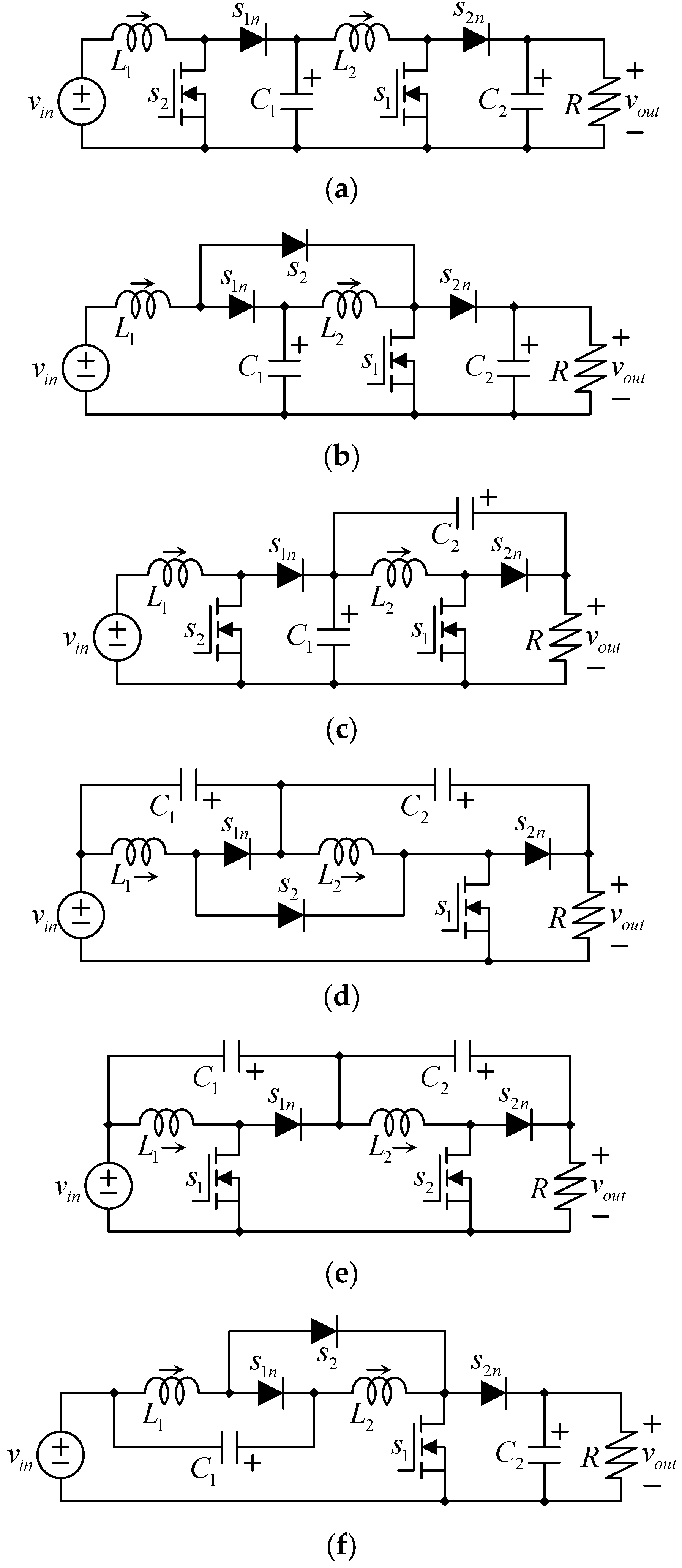
A quadratic boost converter can be synthesized with two cascaded connected boost converters, as shown in
Figure 1a. The well-known single switch quadratic boost topology, initially introduced in [
18], is shown in
Figure 1b. This is now known as the traditional quadratic boost converter; several research works have been dedicated to this topology, including its modelling and control [
19,
20] and the research on other topologies and applications [
21,
22,
23].
Several contributions have been recently proposed in the field of quadratic boost converters. One example is the so-called Multistage-Stacked Boost Architecture (MSBA) Converter (see
Figure 1c), initially introduced in [
24,
25]. It is a quadratic boost converter that can be extended to several levels with the same structure. Some studies have been dedicated to analyzing the size of capacitors and trying to reduce it [
26,
27]. From the input current point of view, it has the same switching ripple as the cascaded boost (
Figure 1a) and the traditional quadratic boost (
Figure 1b).
Another recent contribution in the field is the so-called stackable quadratic boost converter (see
Figure 1d), proposed in [
28]. This topology is based on modular switching stages that can be easily stacked to increase the output voltage gain, achieving an exponential extension of the quadratic boost concept. One of its main advantages is that it requires only a single active switch, and capacitors are rated to a relatively low voltage.
Another recent contribution is the Low Energy Storage Quadratic Boost Converter (LES-QBC) [
29] (see
Figure 1e). This topology, as [
28], requires capacitors rated to a low voltage, but it requires two transistors; in this case, the output voltage has a smaller ripple compared to the single transistor version [
28]. Another relevant contribution is the quadratic boost converter with low buffer capacitor stress (see
Figure 1f), proposed in [
21,
30]. Another quadratic boost converter that reduces on the first capacitor (the buffer capacitor). This allows the use of one small capacitor, but the second capacitor is a normal size (equal to the traditional quadratic boost).
Comparing the different converters recently introduced to the literature, the MSBA converter (
Figure 1c), the traditional topology of quadratic boost (
Figure 1b), and the cascaded boost (
Figure 1a), has a continuous input current. The other topologies sacrifice the continuity of the input current to have an improvement related to the capacitors. And then they obtain a pulsating input current. The MSBA converter and the traditional quadratic boost have as input current the current through
L1, which means that the ac component of its input current is the same as the transistors’ switching frequency, and the input current ripple is determined by the ripple in
iL1.
This article introduces a novel quadratic boost converter topology. The advantage of the proposed converter is that the input current ripple can be reduced compared to the traditional topology. The proposed topology requires an additional inductor and an additional capacitor, but it will be shown with the design example that the inductors in the proposed converter are smaller than in the previous one, and we can consider the second inductor of the quadratic boost was separated into two smaller inductors, which amount of stored energy is the same as that of the first converter inductor. Experimental results are provided to verify the principle of the proposition.
2. The Proposed Converter
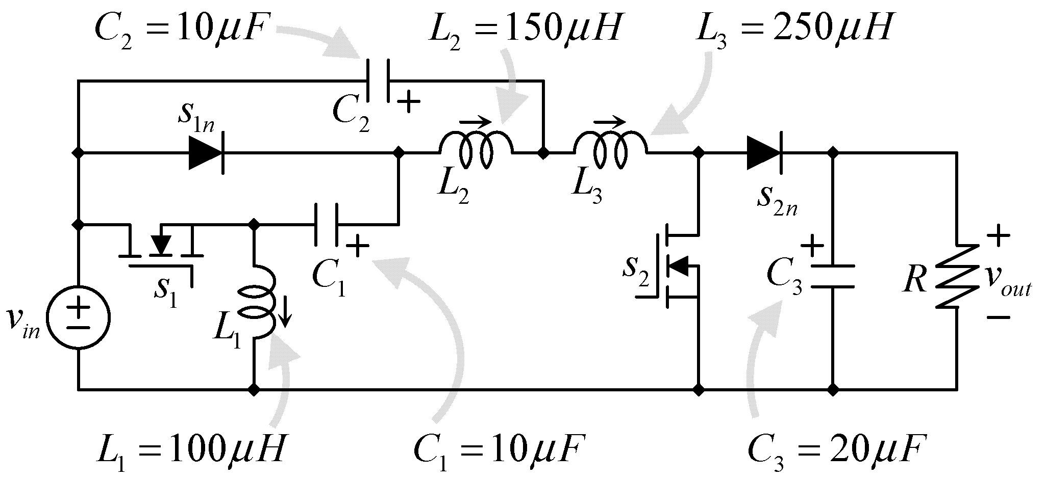
The proposed topology is shown in
Figure 2. It resembles a cascaded connection of an uncommon switching stage followed by a traditional boost converter with an LCL filter between them. The converter has the same number of semiconductors as the quadratic topology in
Figure 1a, but it has more passive components, one capacitor, and one inductor.
As a previous knowledge, we can mention that the
LCL filter (used to link inductors to the utility grid) has two inductors in contrast to the
LC filter, which has only one, but the inductors in the
LCL filter are smaller in size for an equivalent design with the
LC arrangement. One of the purposes of this article is to show that the inductors
L2 and
L3 in
Figure 2 are equivalent in size to
L2 in
Figure 1a,b, with the advantage of providing a smaller input current ripple. But let us start with the topology analysis.
The traditional quadratic boost converter (
Figure 1b) has a single transistor and then two equivalent circuits according to the firing signals state; the proposed converter, similar to the cascaded connection in
Figure 1a, has two transistors and then four equivalent circuits according to the firing signals state.
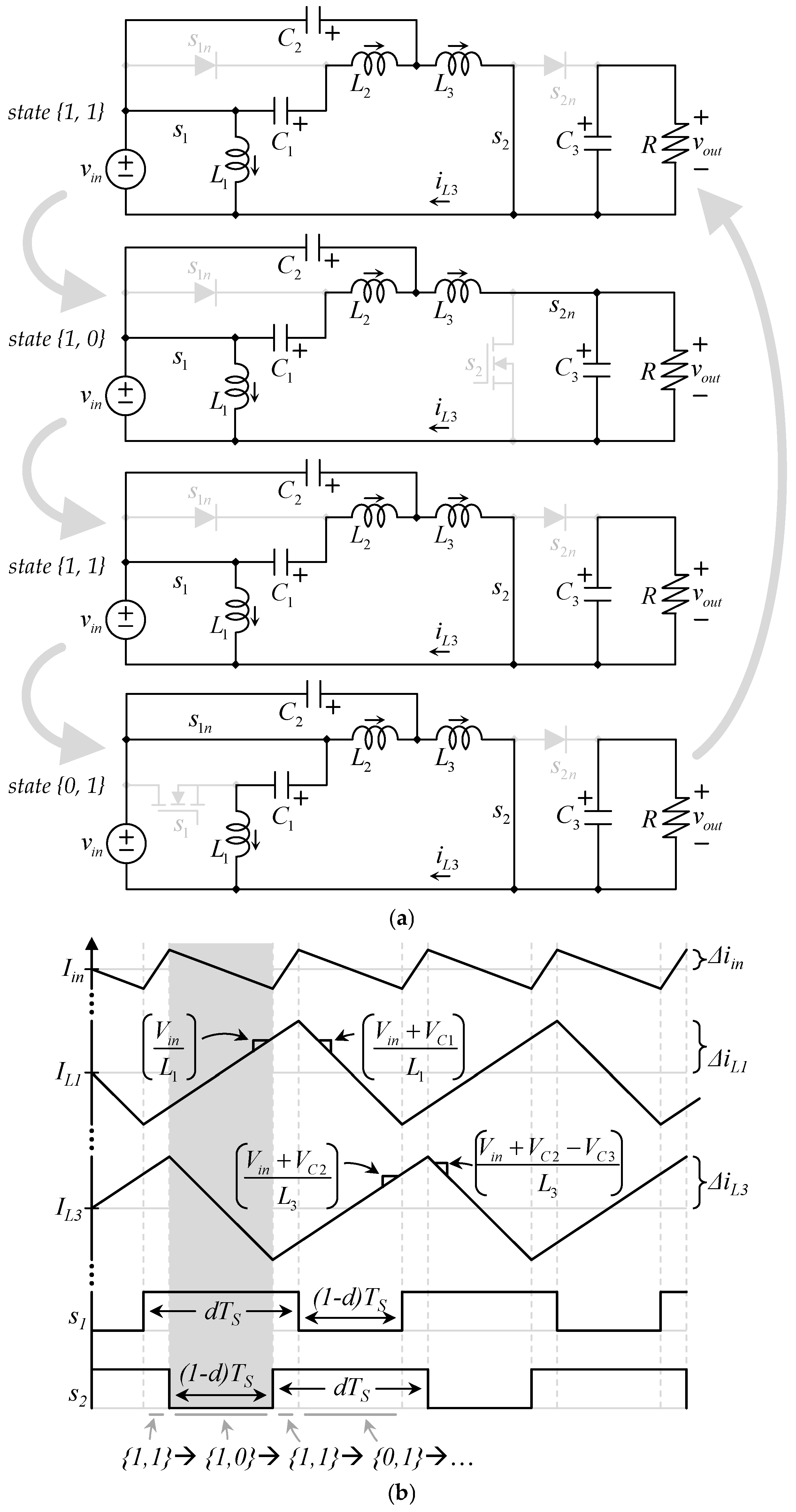
Figure 3 shows those four states.
Let us use the traditional averaging technique to analyze the circuit. The average operation of this converter is relatively simple to determine, since although the converter has four switching states, the charging and discharging state of each of the passive components depends only on one of the transistors.
Let us start with the inductor
L1, which is charged (connected to
vin) when
s1 is closed, regardless of the state of
s2 (see
Figure 3c,d). It also gets discharged with a voltage
vin − vC1 (which is negative since
vC1 >
vin) whenever
s1 is open (see
Figure 3a,b). This leads to the following dynamic averaging equation (considering the transistor
s1 is driven with a duty cycle
d).
Similarly, the inductor
L2 is charged (connected to
vC1 −
vC2) (which is positive since
vC1 >
vC2) when
s1 is closed, regardless of the state of
s2 (see
Figure 3c,d). It also gets discharged by sustaining the voltage −
vC2 whenever
s1 is open (see
Figure 3a,b). This leads to the following dynamic averaging equation (considering the transistor
s1 is driven with a duty cycle
d).
Let us now continue with the last inductor (
L3), which is charged (connected to
vin + vC2) when
s2 is closed, regardless of the state of
s1 (see
Figure 3b,d). It also gets discharged with a voltage
vin + vC2 − vC3 (which is negative since
vC3 > vin + vC2) whenever
s2 is open (see
Figure 3a,c). This leads to the following dynamic averaging equation (considering the transistor
s2 is driven with the duty cycle
d).
Let us start with the capacitors. The capacitor
C1 is discharged (it drains the current
iL2 getting in through its positive voltage side) when
s1 is closed, regardless of the state of
s2 (see
Figure 3c,d). It also gets charged with the current
iL1, whenever
s1 is open (see
Figure 3a,b). This leads to the following dynamic averaging equation (considering the transistor
s1 is driven with the duty cycle
d).
The capacitor
C2 has a non-pulsating current; its current does not depend instantaneously on the switching state, which also happens with the output capacitor of the Cuk and Buck converters. That is an advantage since the capacitance can be relatively low for achieving a certain amount of switching ripple. The dynamic equation for the capacitor
C2 can be written as:
Finally, the last energy storage element in the converter is capacitor
C3. This capacitor gets discharged (with the output current) when
s2 is closed, regardless of the state of
s1 (see
Figure 3b,d). It also gets charged with the difference in current between the inductor
L3 and the output current (
iL1 −
io), which is positive since
iL1 > io). And this happens whenever
s2 is open (see
Figure 3a,c). This leads to the following dynamic averaging equation (considering the transistor
s2 is driven with the duty cycle
d).
In summary, the set of Equations (1)–(6) is the dynamic model of the converter, which can be algebraically simplified and rewritten as (7)–(12)
In all cases, the output current
iout, can be expressed as the output voltage
vout (or
vC3) divided overt the load resistance
R:
In a steady state, the derivatives of the dynamic Equations (7)–(12) are equal to zero, and the equilibrium condition can be obtained as (14)–(19). Note that upper case variables mean the steady state or equilibrium values.
Analysis of the Input Current Ripple
The main advantage of the proposed converter, in contrast with a traditional quadratic boost converter, is that the input current ripple is smaller than the current ripple of the inductor
L1. We will explain this phenomenon by using
Figure 4.
First of all, we can observe in
Figure 4 that the input current of the converter is the summation of two inductor currents (
L1 and
L3), which charge and discharge in an interleaving way.
To formulate the input current ripple, it is important to observe that the input current is always given by the sum of the two (
L1 and
L3) inductor currents, as (20).
The current iL3 has been strategically shown in the ground node of all figures to understand that the output boost and the load can be seen as a super node, and then iL3 is one of the two currents composing the input current iin (along with iL1).
Then we can consider the sequence of equivalent circuits that results when the converter is operating (see
Figure 4a) from the switching signals
s1 and
s2. (see
Figure 4b (bottom)). By following the switching sequence, the charging and discharging slopes of inductors
L1 and
L3 can be determined for each switching state. Summing these two inductor currents yields the input current, whose ripple can then be deduced.
In particular, according to the switching pattern shown in the shaded time interval of
Figure 4a, this analysis leads to the expression of the input current ripple given in Equation (21).
It is important to notice that although the expression in (21) is the summation of two ripples, one of them is positive (since
Vin is positive), while the other one is negative since (
Vin + VC2 − VC3) is negative. This can be corroborated by summing
Vin + VC2.
Equation (22), which shows the sum of Vin + VC2 as a function of Vin and the duty cycle D, can be compared with VC3 in (16), in the same terms, and we can conclude that (22) is always smaller than (16).
This effect can also be explained in
Figure 4b by observing the cancellation mechanism between
iL1 and
iL3. If a traditional quadratic boost converter is made with the same value in
L1. And since both converters have the same duty cycle (for the same gain). This converter always has a smaller input current ripple. The traditional quadratic boost converter would have
iL1 in
Figure 4b as input current, and the proposed converter has the cancelling component in
iL3. This will also be observed in the simulation and experimental results.
Another fact that can be appreciated by observing
Figure 4 is that the frequency of the current ripple at the input side differs from the traditional quadratic boost converter. In the traditional case, the input current corresponds to the current of a single inductor, so its ripple appears at the switching frequency. In contrast, in the proposed topology, the input current is the sum of two interleaved inductor currents (
iL1 + iL3), which are phase-shifted due to the switching sequence. This interleaving not only reduces the net ripple amplitude but also shifts the dominant ripple component to twice the switching frequency, which makes it easier to filter if additional attenuation is required.
3. Comparisons with Other Topologies
This section presents a comparative analysis of different quadratic converter topologies. There are several quadratic boost topologies in the literature, as shown in
Figure 1; some of them have discontinuous (pulsating) input current. In terms of input current ripple, the traditional topology, along with the proposed one, and the MSBA converter are superior to those that have discontinuous input current. Then those three converters will be considered for the comparison. The adopted methodology begins with the traditional quadratic boost converter as a baseline, from which alternative configurations are designed with comparable characteristics in terms of components, stored energy, and switching ripple. Advantages and disadvantages of the different architectures are then discussed.
3.1. The Traditional Quadratic Boost Converter
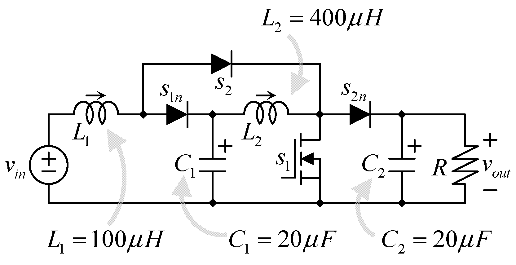
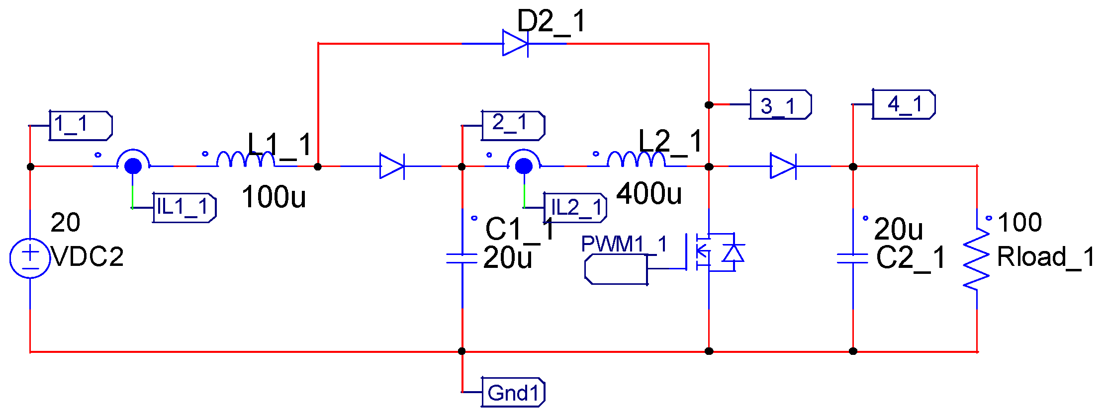
Let us consider the traditional topology as shown in
Figure 5.
L1 (100 μH) is the inductor with the larger current; it carries the input current plus the switching ripple, which results in 10.51 A. Inductor
L2 (400 μH) drains a maximum current of 4.37 A, including the switching ripple. Both capacitors are 20 μF;
C1 is rated at 63.08 V, while
C2 is rated to the output voltage in this case, 156.48 V, including the switching ripple.
Table 1 summarizes the parameters of the traditional quadratic boost converter.
3.2. The MSBA Converter
Let us continue with the Multistage-Stacked Boost Architecture (MSBA) Converter, as shown in
Figure 6. The structure is similar to the traditional one. It has two inductors that draw the same amount of current as in the previous case, and then they were chosen to have the same inductance.
L1 (100 μH) is the inductor with the larger current; it carries the input current plus the switching ripple, which results in 10.51 A. Inductor L2 (400 μH) drains a maximum current of 4.37 A, including the switching ripple. Both capacitors are 20 μF; C1 is rated at 63.08 V. The main advantage of the MSBA is that the second capacitor C2 is not rated to the output voltage; in this case, it is rated to 93.75 V, including the switching ripple.
The reduction in the voltage rating of the second capacitors results in a reduction in the total stored energy in the capacitors. From 283 mJ to 127 mJ. We can summarize that the second capacitor is smaller since it is rated for a lower voltage. Their output voltage ripple is still similar, in the order of 0.2 V.
Table 2 summarizes the parameters of the traditional quadratic boost converter.
3.3. The Proposed Converter
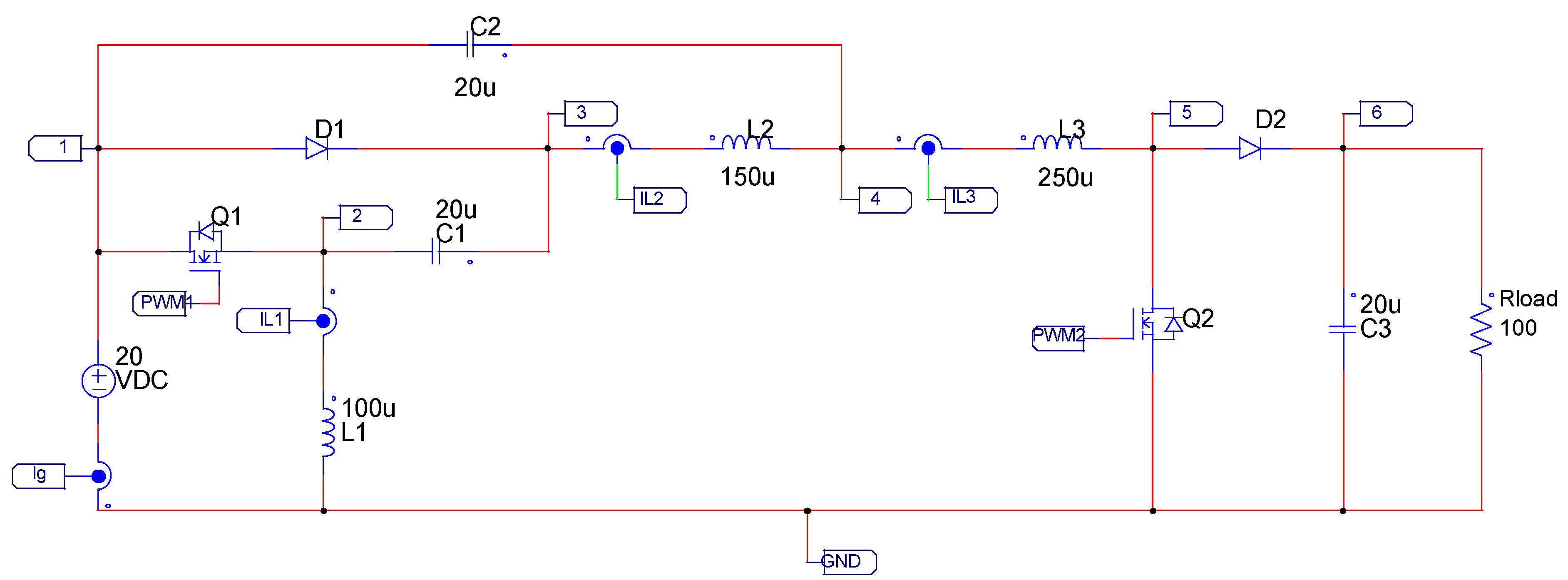
Let us continue with the proposed converter, as shown in
Figure 7. It has three inductors. The first inductor was chosen to have the same inductance
L1 (100 μH) as in the traditional case, but in this case, it is rated to a lower current; it drains 6.6 A Considering the ripple, this is because their current is lower than the input current; it is basically the input minus the output current. Leading to a smaller inductor in
L1.
The proposed converter has the second inductance separated into two different inductors L2 and L3. Although they drain the same DC current, their switching ripple differs, and then they are rated to a different maximum current considering the ripple; in this case, L2 (150 μH) is rated to 5.9 A, and L3 (250 μH) is rated to 4.65 A. Still, the total stored energy in inductors is 7.5 mJ, less than the 9.4 mJ in the other two converters. That means the inductors are smaller. But also, the Input current ripple is smaller as described in the previous section.
The stored energy in capacitors is similar but slightly lower, 270 mJ, compared to the 283 mJ in the traditional design.
Table 3 summarizes the parameters of the proposed converter in the described design. Capacitors are rated in the following manner:
C1 (10 μF) is rated to 64.25 V,
C2 (10 μF) is rated to 38.78 V, and
C3 (20 μF) is rated to 156.48 V.
We can conclude that the proposed converter has a similar capacitor size to the traditional topology. The MSBA converter is the winner in this parameter; the main contribution of the proposed converter comes from the inductor’s perspective. It has smaller inductors, and also smaller input current ripple.
4. Simulation Validation
A simulation was performed with the traditional converter with the parameters described in
Figure 5, including a switching frequency of 150 kHz, a load resistance of 100 Ω, and
D = 0.6. And with the proposed converter with the parameters described in
Figure 7. The simulations were carried out using the professional version of PSIM (version 2022.1.0.8, Powersim Inc., Rockville, MD, USA). This software environment was selected because of its robust library of power electronics components and its capability to accurately model switching converters.
Figure 8 shows the traditional quadratic boost converter schematic in PSIM.
Figure 9 shows the proposed topology schematic in PSIM. Both converters were simulated with the same switching frequency, voltage gain, and load.
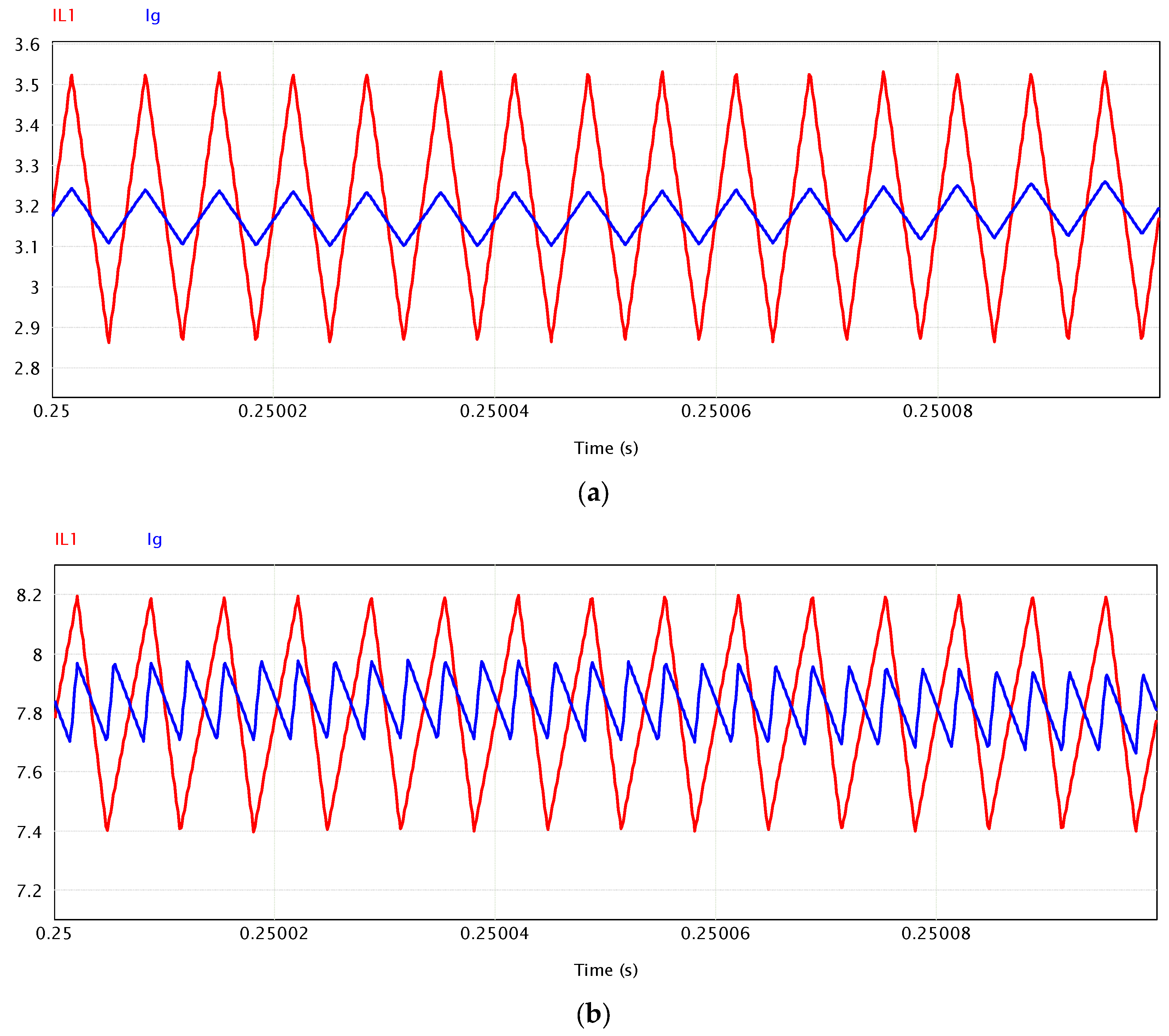
Figure 10 shows the input current ripple of both converters under two different conditions.
Figure 10a shows the input current ripple of the proposed converter (blue) compared with the input current ripple of the traditional quadratic boost converter (red), for the described operation with a duty cycle of
D = 0.5. The traditional quadratic boost converter has an input current ripple of 0.325 A (0.65 A peak-to-peak), while the proposed converter has an input current ripple of 0.065 A (0.13 A peak-to-peak). The proposed converter, with equivalent components, has 20% of the ripple of the traditional converter when
D = 0.5.
Figure 10b shows the input current ripple of the proposed converter (blue) compared with the input current ripple of the traditional quadratic boost converter (red), for the described operation with a duty cycle of
D = 0.6. The traditional quadratic boost converter has an input current ripple of 0.4 A (0.8 A peak-to-peak), while the proposed converter has an input current ripple of 0.125 A (0.25 A peak-to-peak). The proposed converter, with equivalent components, has 31% of the ripple of the traditional converter when
D = 0.6.
5. Experimental Validation
The converter shown in
Figure 7 was built and tested to corroborate the performance of the circuit using the same components as summarized in
Table 4.
Figure 11 shows the experimental prototype.
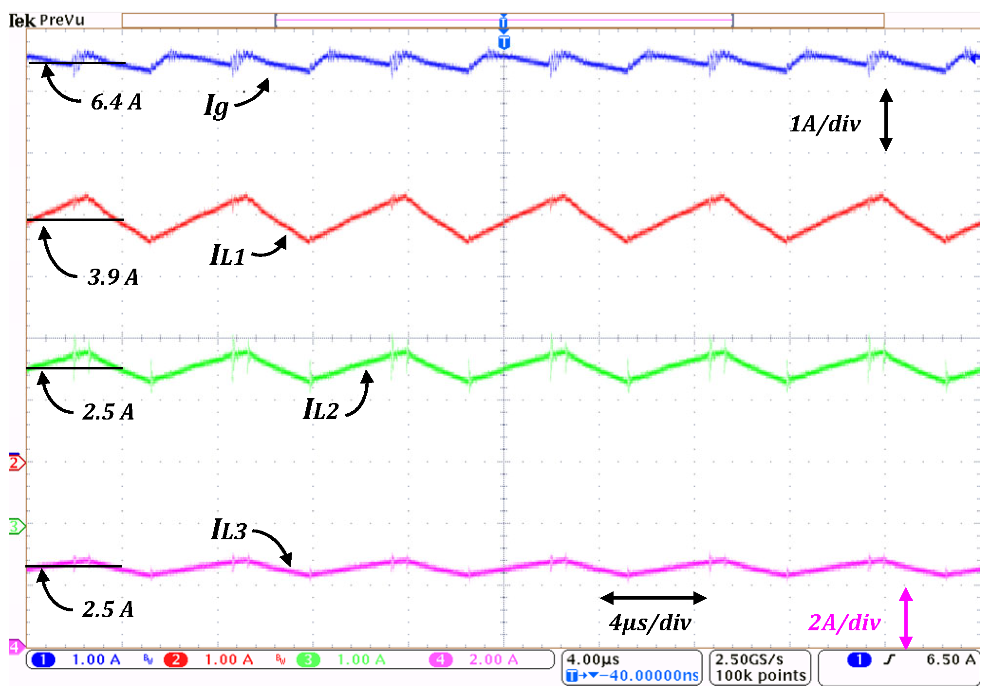
Three tests were carried out to verify the performance under different conditions. The first one under nominal, input voltage/load conditions, the second one considering input voltage variations, and the third one under load variations. For the first test, the nominal conditions (
Vin = 20 V,
Vo = 100 V, and
R = 100 Ω) were used to obtain the input current and the currents through the inductors, which are shown in
Figure 12.
Figure 13 shows the voltage across capacitors
C1,
C2, and
C3, respectively.
As can be seen in
Figure 12, the average current through all the inductors is smaller than the input current, with values ranging from 3.7 A for
L1 to 2.4 A for
L3. The input current has an average value of 6.2 A with a ripple of 0.5 A, which is smaller than the inductor’s current ripples. It is worth noticing that the frequency of the input current ripple is twice the switching frequency. The obtained measurements are consistent with Equations (14)–(16), which allows us to corroborate that capacitors
C1 and
C2 hold a fraction of the output voltage.
The transistors used in the proposed prototype are Gallium Nitride (GaN) devices, which are capable of switching at very high frequencies, even in the range of megahertz [
31]. Still other devices, like inductors in DC-DC converters for the range of hundreds of watts, are designed to operate in the range of hundreds of kilohertz. In this case, the prototype is based on the board [
32], the base board to develop some commercial converters like [
33], whose switching frequency is 100 kHz. During the design process, the switching frequency of the converter was selected as 150 kHz.
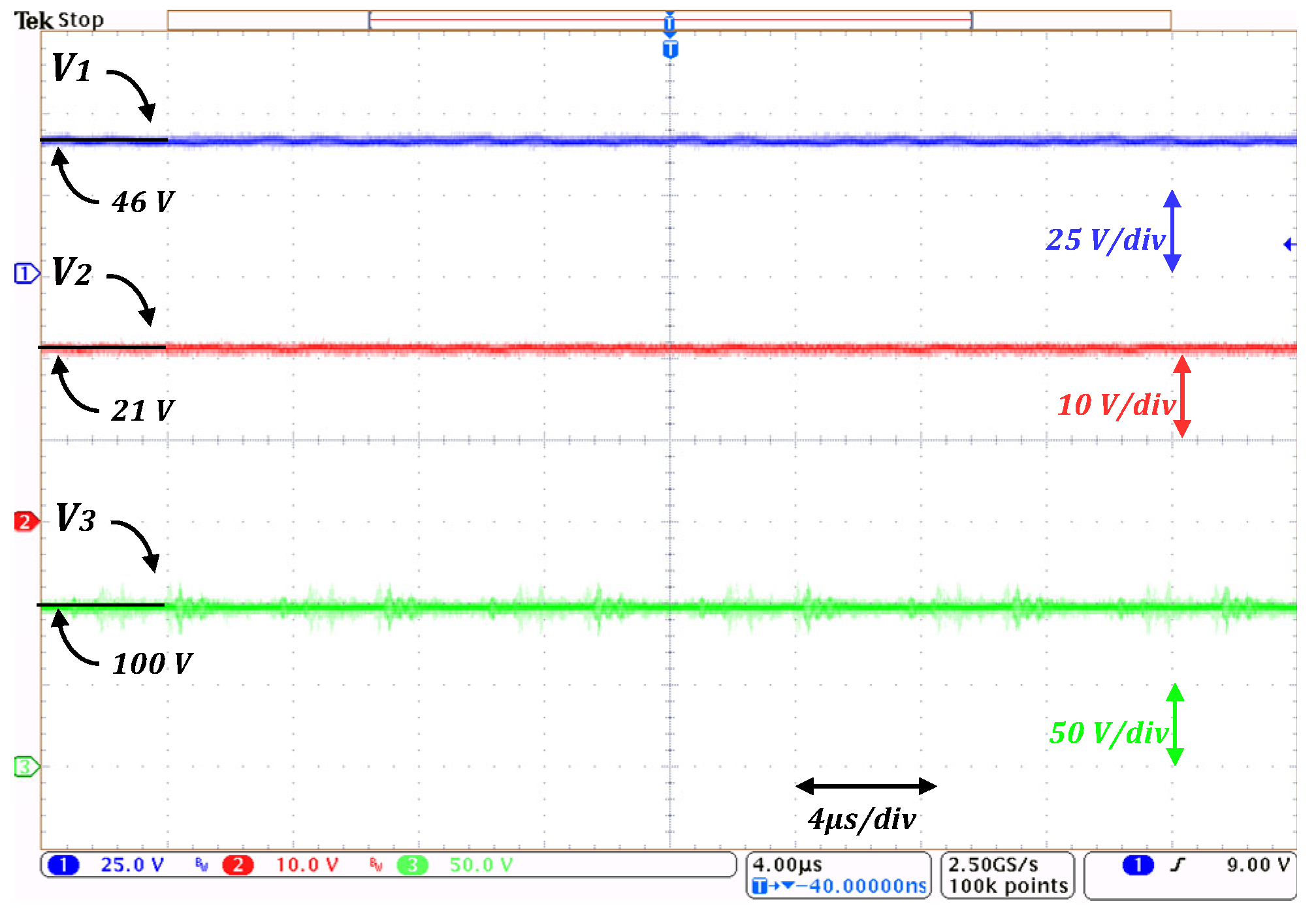
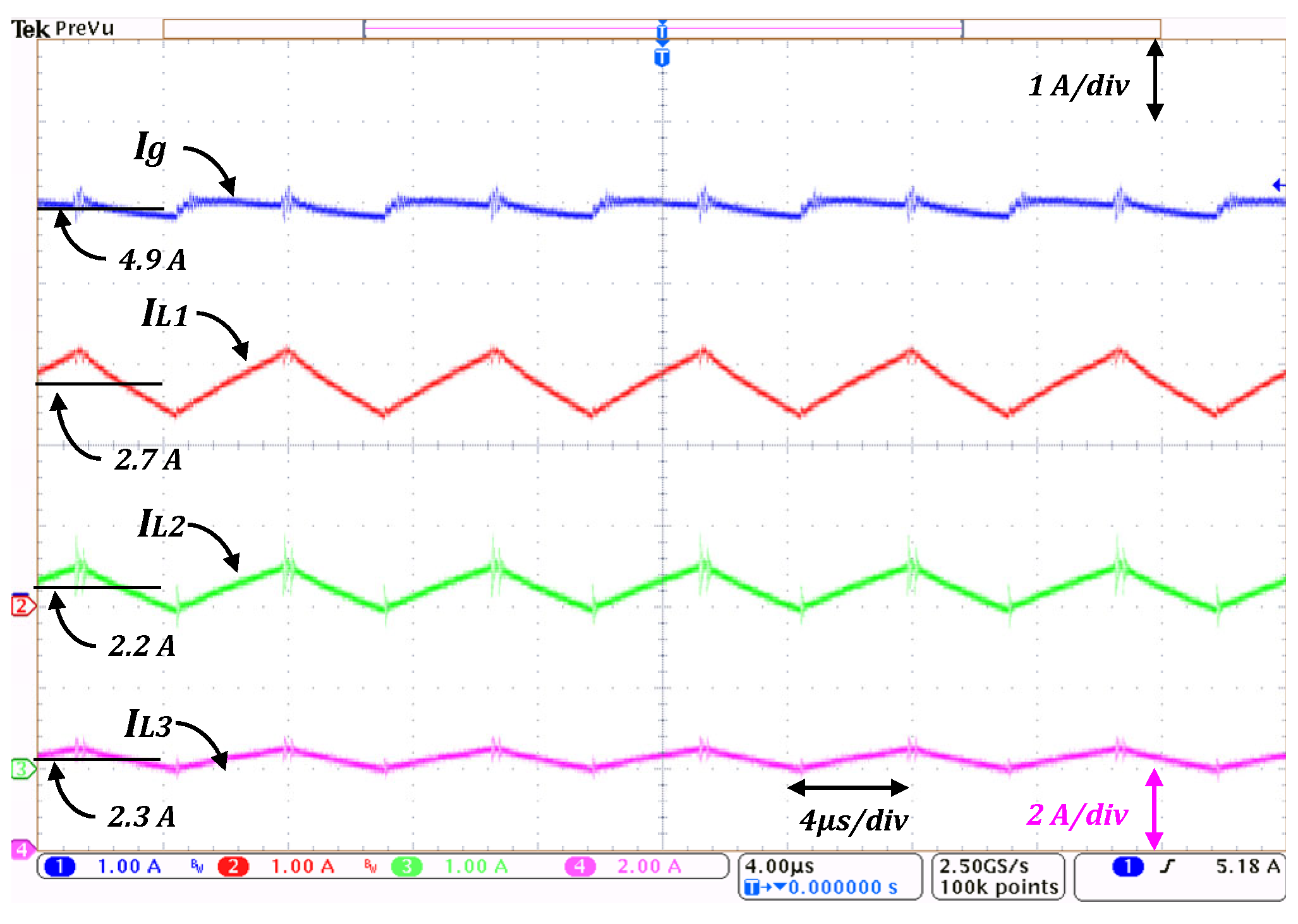
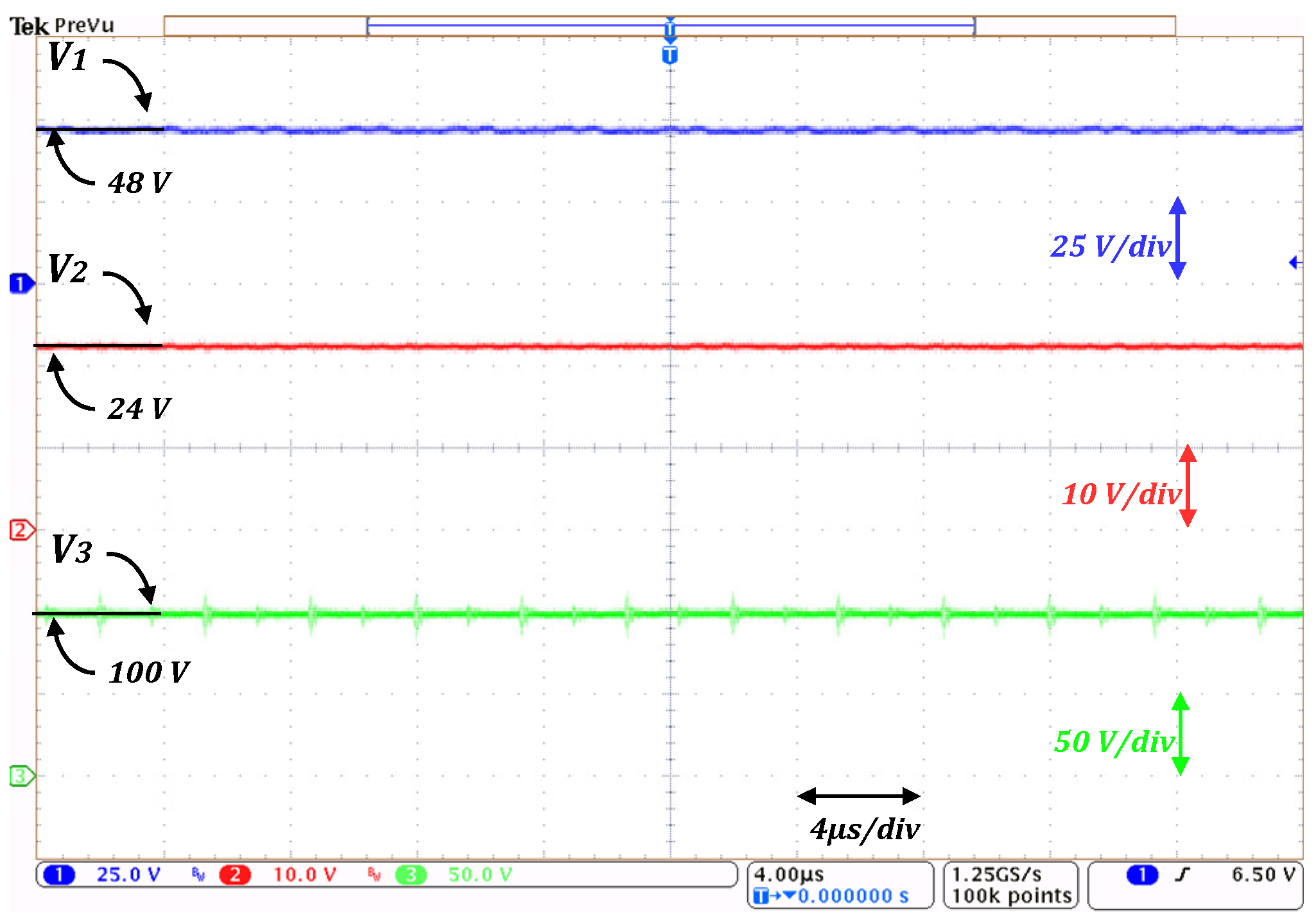
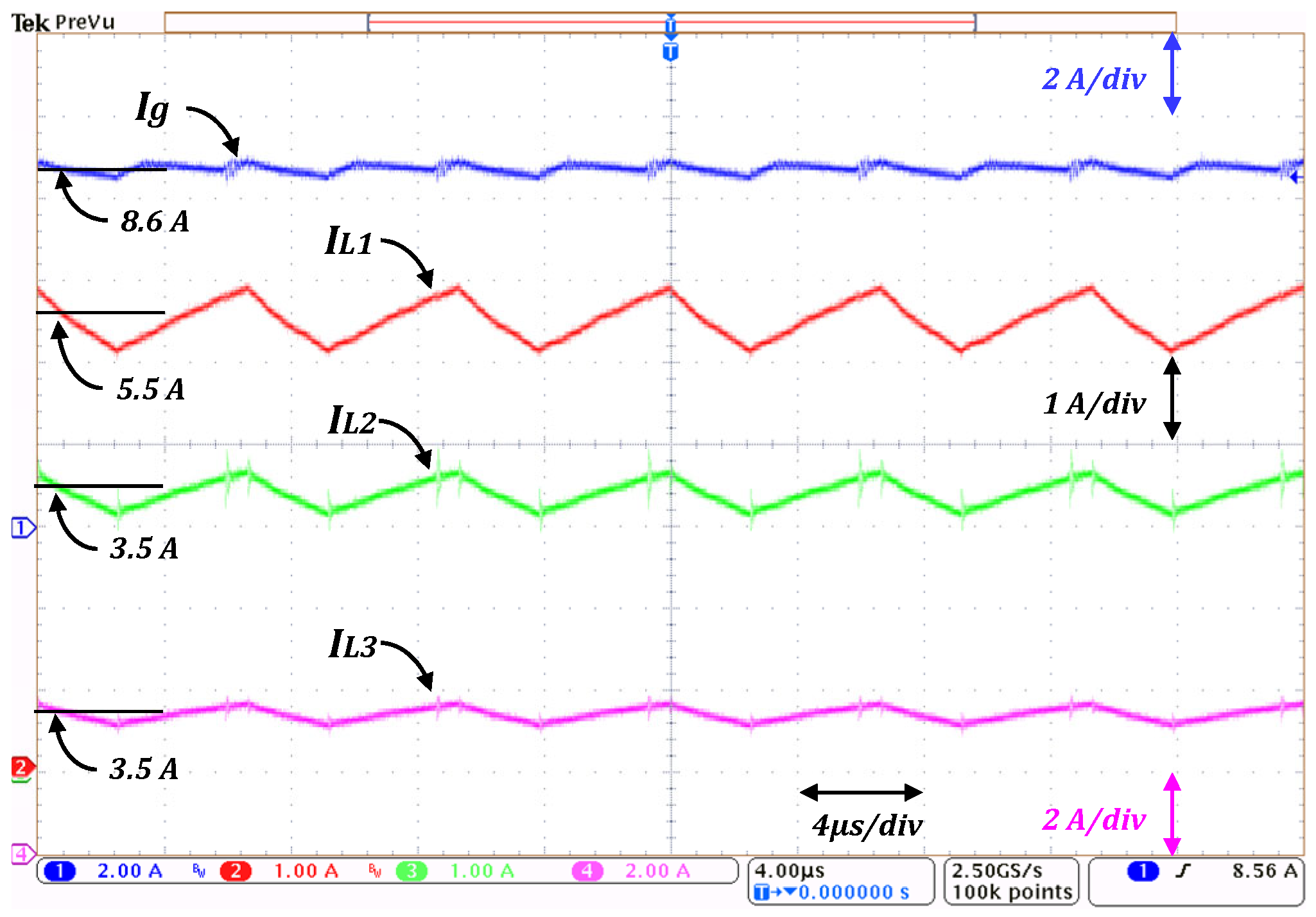
The second test considers the variation in the input voltage within a range of ±25%.
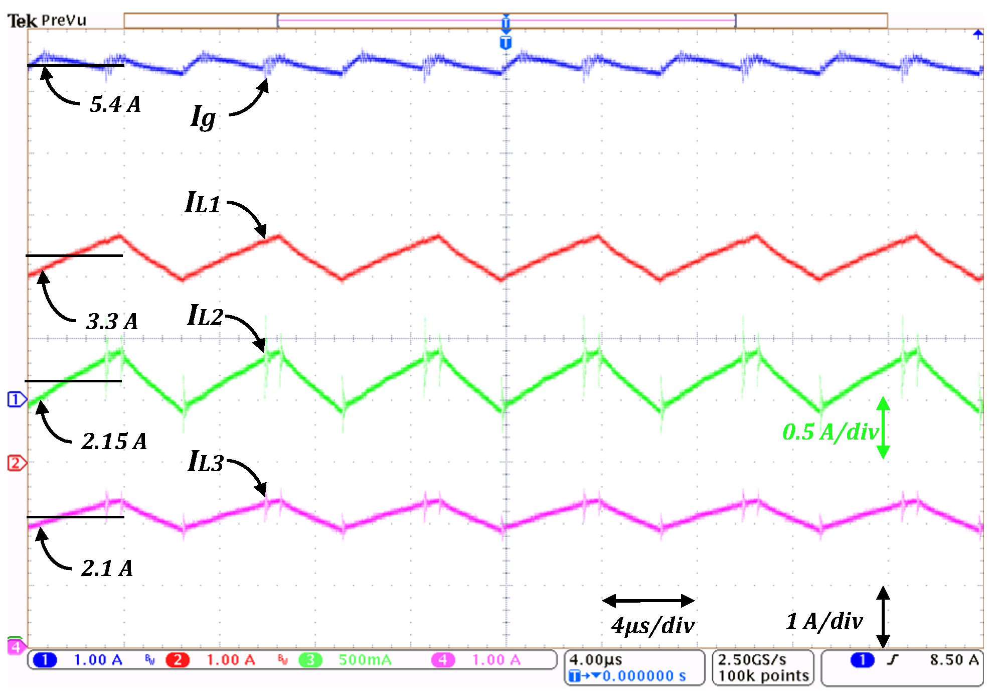
Figure 14 shows the experimental waveforms of the input current and current through inductors for an input voltage
Vin = 15 V. The load was kept at 100 Ω, and the duty cycle was adjusted to maintain the 100 V output voltage. As can be seen, average current values increased significantly, but the input current ripple remains small compared to the inductor’s current ripple.
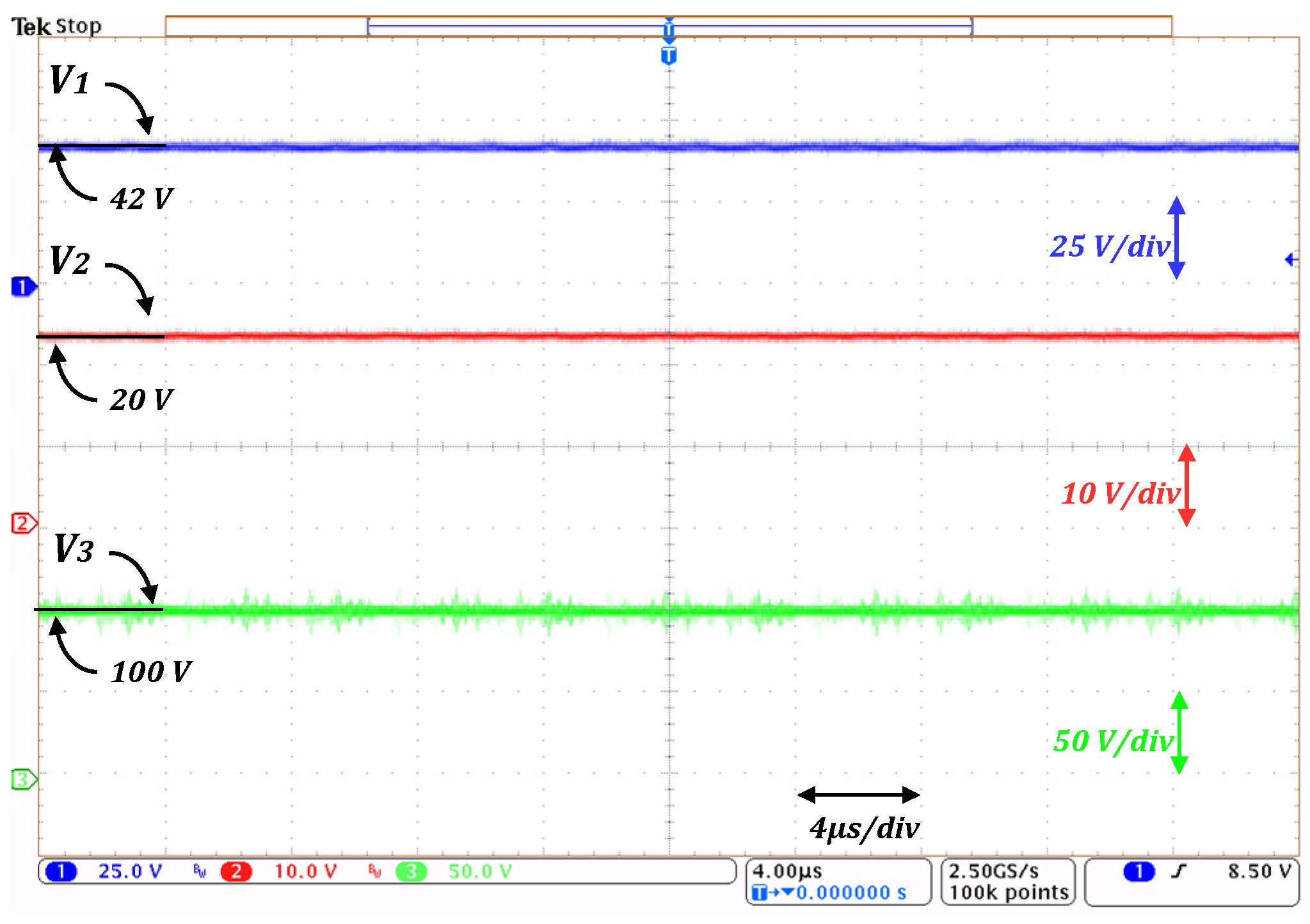
Figure 15 shows how the capacitor’s voltage magnitudes are affected by the decrease in the input voltage.
Current waveforms in
Figure 16 correspond to the 25 V input voltage variation. It can be noticed in
Figure 16 that the average magnitudes are in sharp contrast with those obtained in the previous experiment; however, although there exists some difference in the inductor’s current ripple magnitudes, the input current ripple remains small.
The corresponding capacitors’ voltage waveforms for these experiments are shown in
Figure 17; the output voltage, which corresponds to the voltage across capacitor
C3, is fixed at 100 V by adjusting the duty cycle again, which also affects the voltage held by
C1 and
C2.
In the third test, the load resistor was changed within a ±25% range. First, the load resistor was reduced to 75 Ω; see
Figure 18.
The average values of the input and inductor current in
Figure 18 increased substantially compared to the nominal referenced values, but as in the previous test, the input current ripple represents a portion of the inductor’s current ripple magnitudes.
Voltages across capacitors are shown in
Figure 19; there are small level changes in
V1 and
V2 due to the change in
D (to keep the output voltage at 100 V).
Finally, the load resistor was increased to 125 Ω.
Figure 20 shows the current waveforms for this experiment.
As expected, the average current levels are smaller in
Figure 20 compared to the base parameters, and the inductor’s current ripple magnitudes are bigger than the input current ripple; this is mainly due to the cancellation of the ripples among inductors.
Figure 21 show the voltage across the capacitors for this experiment.
Figure 22 and
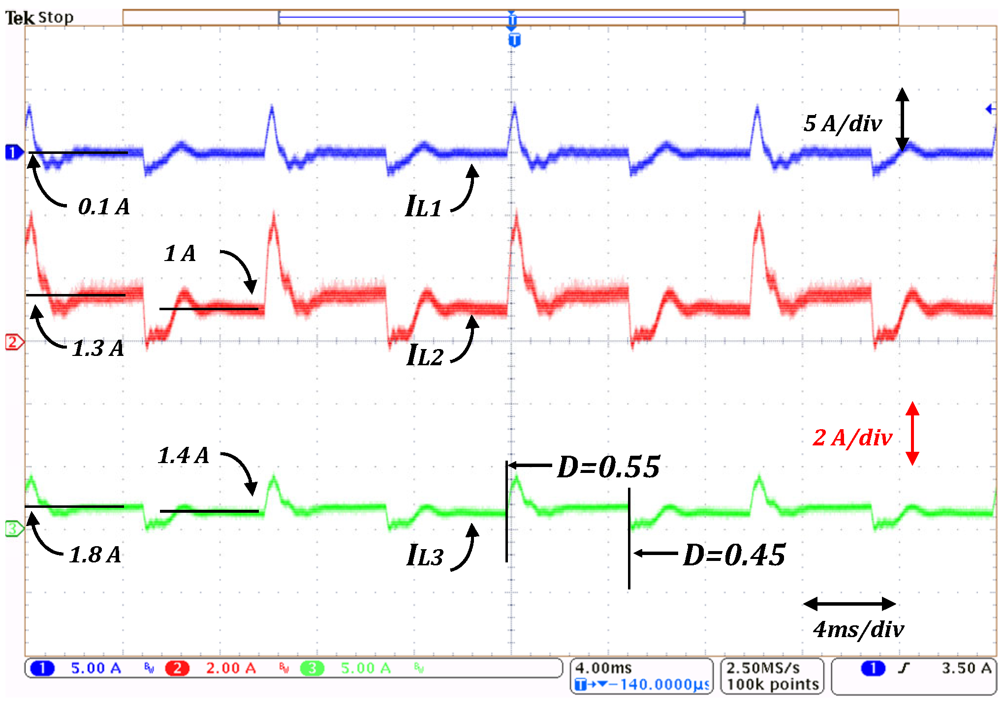
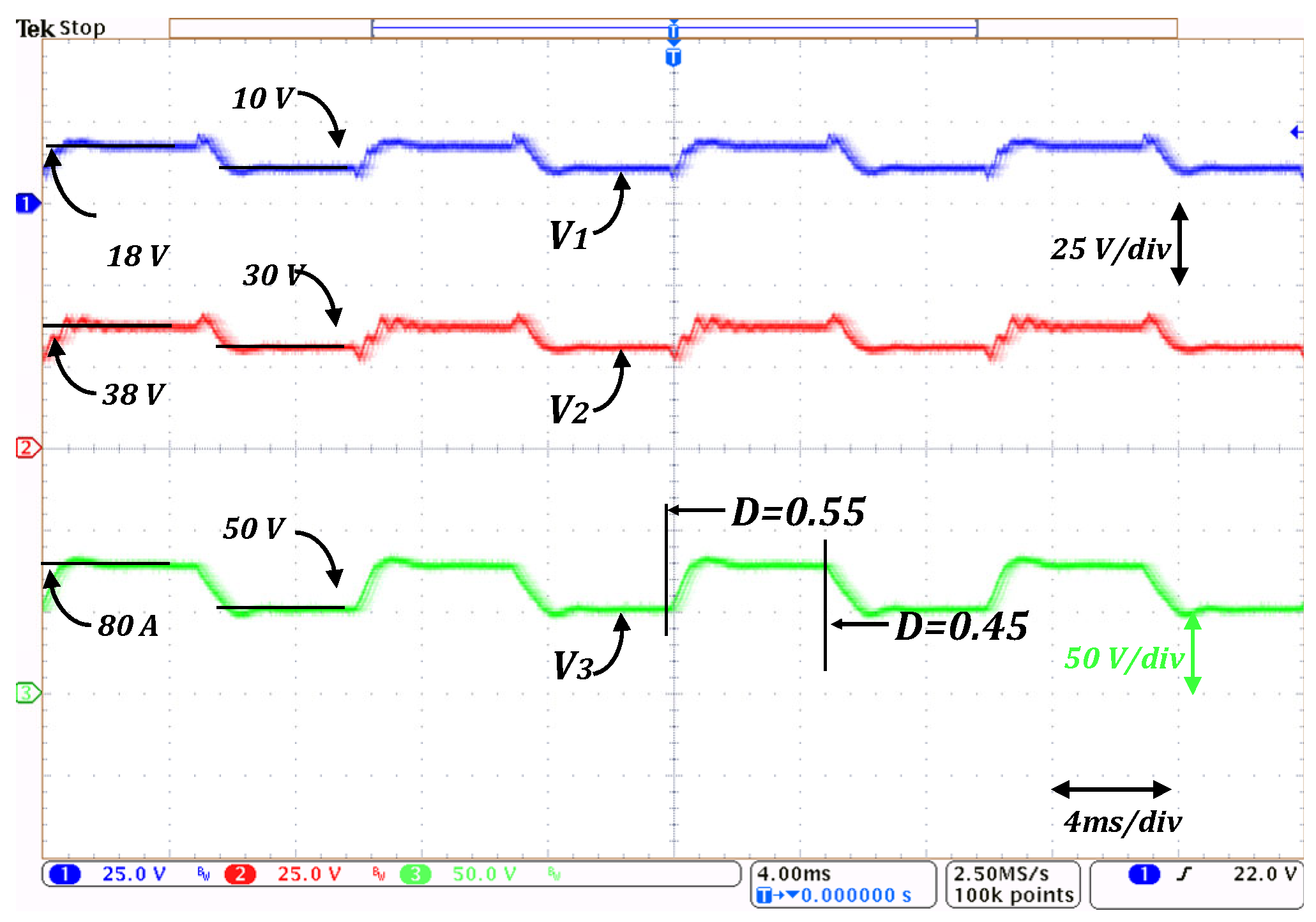
Figure 23 present the experimental results of the proposed converter when subjected to duty cycle variations every 5 ms, with input voltage
, output voltage
, and load resistance
. The test was designed to evaluate the converter’s transient performance and dynamic stability in an open loop when the duty ratio changes between
and
.
Notice that the proposed converter responds rapidly and predictably to duty cycle perturbations, maintaining a stable operation without significant overshoot or oscillation. This validates the converter’s dynamic robustness and its suitability for applications requiring fast control action and reliable voltage regulation under varying operating conditions.
