Article

A High-Performance Ka-Band Cylindrical Conformal Transceiver Phased Array with Full-Azimuth Scanning Capability

1
The School of Electronic and Information Engineering, Xi’an Jiaotong University, Xi’an 710049, China
2
The Key Laboratory of All Optical Network and Advanced Telecommunication Network of Ministry of Education, Institute of Lightwave Technology, Beijing Jiaotong University, Beijing 100044, China
*
Author to whom correspondence should be addressed.
Appl. Sci. 2025, 15(16), 8982; https://doi.org/10.3390/app15168982
Submission received: 16 July 2025 / Revised: 13 August 2025 / Accepted: 13 August 2025 / Published: 14 August 2025

Abstract

This paper presents a Ka-band cylindrical conformal transceiver active phased array (CCTAPA) with a full-azimuth scanning gain fluctuation of 0.8 dB and low power consumption. The array comprises 20 panels of 4 × 4 antenna elements, RF beam-control circuits, a Wilkinson power divider network, and frequency converters. The proposed three-subarray architecture enables ±9° beam scanning with minimal gain degradation. By dynamically switching subarrays and transceiver channels across azimuthal directions, the array achieves full 360° coverage with low gain fluctuation and power consumption. Fabrication and testing demonstrate a gain fluctuation of 0.8 dB, equivalent isotropically radiated power (EIRP) between 50.6 and 51.3 dBm, and a gain-to-noise-temperature ratio (G/T) ranging from −8 dB/K to −8.5 dB/K at 28.5 GHz. The RF power consumption remains below 8.73 W during full-azimuth scanning. This design is particularly suitable for airborne platforms requiring full-azimuth coverage with stringent power budgets.

1. Introduction

With the rapid advancement of electronics and information technologies, there is an increasing demand for all-weather, all-domain network communication, making the realization of comprehensive communication capabilities on aerial platforms, satellite terminals, and 5G mmWave base stations increasingly imperative [1,2,3,4,5], which collectively establish the application-driven demand for conformal phased arrays in these platforms. In aerial platforms, satellite terminals, and 5G mmWave base stations applications, traditional phased arrays [6,7,8,9,10,11,12] demonstrate inherent constraints including limited wide-angle scanning capability, significant gain loss during scanning, an inability to achieve shared-aperture transmit–receive functionality, and high array power consumption. To overcome these limitations, a conformal phased-array antenna with full-azimuth coverage, low gain variation, shared-aperture transmit–receive capability, and low power consumption offers a quite good solution.
Phased-array antennas [13] can be classified into active phased-array antennas and passive phased-array antennas. Passive phased-array antennas are inadequate for modern applications due to their excessive loss and inferior performance characteristics. Wide-scan active phased arrays can be categorized into planar and conformal configurations. Planar active phased arrays [14,15,16,17] predominantly employ microstrip antenna designs with low-profile characteristics but suffer from significant gain degradation at wide scan angles, high power consumption, and inability to achieve full-azimuth scanning. Conformal phased arrays are indispensable for platforms demanding wide-angle coverage. Unlike planar arrays, which exhibit a >3 dB scan loss beyond ±60° [14,15], cylindrical or spherical conformality maintains near-constant aperture projection. This enables full-azimuth coverage without mechanical rotation—critical for aerial platforms, satellite terminals, and 5G mmWave base stations. Conformal arrays are categorized into many fundamental geometric types: spherical, cylindrical, conical, wing-conformal, and flexible arrays. Spherical phased arrays feature wide-angle scanning capability, low gain fluctuation, and platform-conformal integration [18,19,20,21,22,23,24,25,26,27]. Ref. [23] presents an active spherical array with X-band waveguide-fed elements, requiring 25% active unit excitation for beam scanning with full-azimuth coverage. Ref. [24] describes an S-band spherical array using a 3D-printed frame, achieving hemispherical scanning through optimized distribution of 23 elements. Cylindrical conformal arrays offer wide-angle scanning and structural conformality to carriers [28,29]. The Ku-band flexible active conformal array in [28] achieves ±60° scanning with 3 dB gain variation at 1.068 W/element power consumption. Ref. [29] proposes a low-profile cylindrical X-band array enabling ±60° scanning with a >3 dB gain fluctuation. Conical conformal antennas exhibit complex feed networks [30]. Ref. [31] introduces a wing-conformal array capable of ±60° scanning with >2 dB scan loss. A flexible foldable array for 5G mmWave [32] provides 360° azimuthal scanning, while elevation coverage is mechanically adjusted through folding for hemispherical coverage. Ref. [33] develops a Ka-band foldable LCP active array that extends the scanning range via structural deformation, combining electronic steering for multi-mode radiation while balancing gain and coverage.
This paper proposes a cylindrical conformal active phased-array antenna (see Figure 1a) featuring full-azimuth coverage, minimal scan loss, shared-aperture transceiver, simplified architecture, and low power consumption. Compared with spherical arrays, the cylindrical conformal array proposed in this work employs dynamic subarray switching technology, activating only 15% of elements to reduce power consumption by over six times. It achieves higher integration density through high-density PCB technology while maintaining structural simplicity, enhanced reliability, and lower cost. Versus conical and wing-conformal arrays, the proposed cylindrical design utilizes tri-face beamforming for ±9° scanning and electrical subarray switching to enable full-azimuth 360° coverage with 0.8 dB gain fluctuation. Employing a partitioned architecture with separated antenna modules and RF beam-control modules, this design simplifies structural implementation and feed network configuration while reducing production costs. Relative to flexible foldable arrays [32,33], the fixed cylindrical structure simplifies calibration/control and delivers full-azimuth coverage. PCB-based fabrication facilitates mass production while offering superior power efficiency and reliability.
This paper is organized as follows: Section 1 briefly introduces the research background of wide-angle scanning conformal active phased-array antennas and the existing conformal phased-array solutions. Section 2 details the conformal array architecture, including the antenna array design, transceiver channel implementation, power divider network, and measurement of RF beam-control module parameters such as gain, P1dB, and noise figure, as well as EIRP and G/T calculations. Section 3 presents the simulation, fabrication, and experimental validation. Finally, Section 4 concludes the work.

2. Cylindrical Conformal Phased-Array Design

The Ka-band CCTAPA consists of an antenna array, RF beam-steering circuitry, and a frequency converter (see Figure 1a). The antenna array is composed of 20 subarrays, each configured as a 4 × 4 array of antenna elements. The Ka-band CCTAPA features electronically scanned azimuth beams with fixed-elevation coverage. Elevation beamforming is achieved through 4:1 Wilkinson power dividers for equal-amplitude in-phase combining. The RF beam-steering circuit utilizes a PCB-integrated solution [34] for the cost-effective, high-density integration of RF and control circuits. The circular frequency converter features vertical interconnects with the RF control board. In receive mode, signals passing through an 8-channel beamforming chip (providing LNA, phase shifting, and attenuation) are combined via switches and LNAs then aggregated through a 10:1 network before downconversion. The transmit path follows the reverse sequence (see Figure 1b).
The PCB stackup was constructed utilizing Panasonic Megtron7 material, characterized by a relative dielectric permittivity (ϵr) of 3.35 and a dissipation factor (tanδ) of 0.003 at 29 GHz, as illustrated in Figure 1c. The RF beamforming network (BFN) was implemented in Layer M1, while Layer M2 served as the ground plane. Layer M12 was predominantly allocated for the beam-control circuitry integrated with the FPGA. The M3~M11 layers were designated for digital control signals, power distribution, and ground. Surface-mount technology (SMT)-compatible components were employed in the design, with placement on both Layer M1 and Layer M12. The overall thickness of the PCB measures approximately 2 mm.

2.1. Antenna Array Design

Figure 2a shows the 3D model of a linearly polarized L-probe-fed metasurface patch antenna unit cell and the radiation pattern of the antenna element. The metasurface introduces additional closely spaced resonant modes beyond the fundamental resonance of the primary driven patch. Electromagnetic coupling between the driven patch and metasurface elements effectively combines these multiple resonances, creating a seamless and broader operational bandwidth. This presents a distinct contrast to conventional stacked patches, which typically rely solely on coupling between two primary patch resonances. In this array antenna design, metasurface-based architecture was selected to ensure superior gain flatness across the extended bandwidth while mitigating bandwidth degradation effects caused by array coupling during beam scanning operations. The metasurface patch antenna was selected for its low profile, ease of integration, and wideband characteristic. While conventional single-patch microstrip antennas typically exhibit about 5% impedance BW, the proposed L-probe-fed metasurface patch antenna achieves 10–20% BW [35], successfully covering the wideband range of 26–31 GHz.
The array elements were positioned on a square grid, spaced 7 mm apart, corresponding to 0.72 free-space wavelengths at 31 GHz. A square grid was chosen for its simplicity in implementation. The grid spacing of 0.72 λ was selected to balance the array scanning angle and maximize the array gain. The array unit is fabricated using a cost-effective Taconic TYL-5 substrate with a relative dielectric permittivity ϵr = 2.2 and a dissipation factor tanδ = 0.009. The substrate comprises two dielectric layers and one prepreg layer, with thicknesses of 1.52 mm, 0.76 mm, and 0.2 mm, respectively, as detailed in Figure 2a. The performance simulation of the antenna unit is presented in Figure 2b. The antenna unit exhibits excellent impedance-matching characteristics, demonstrating a −10 dB reflection coefficient bandwidth from 21.5 to 35 GHz (47.8% fractional bandwidth). The antenna unit maintains a stable gain between 5.8 dB and 7.5 dB across the operational bandwidth. The phased array operates across 26–31 GHz with reflection coefficients below −17 dB and gain stability between 6.9 and 7.5 dB, demonstrating broadband performance with consistent radiation characteristics.
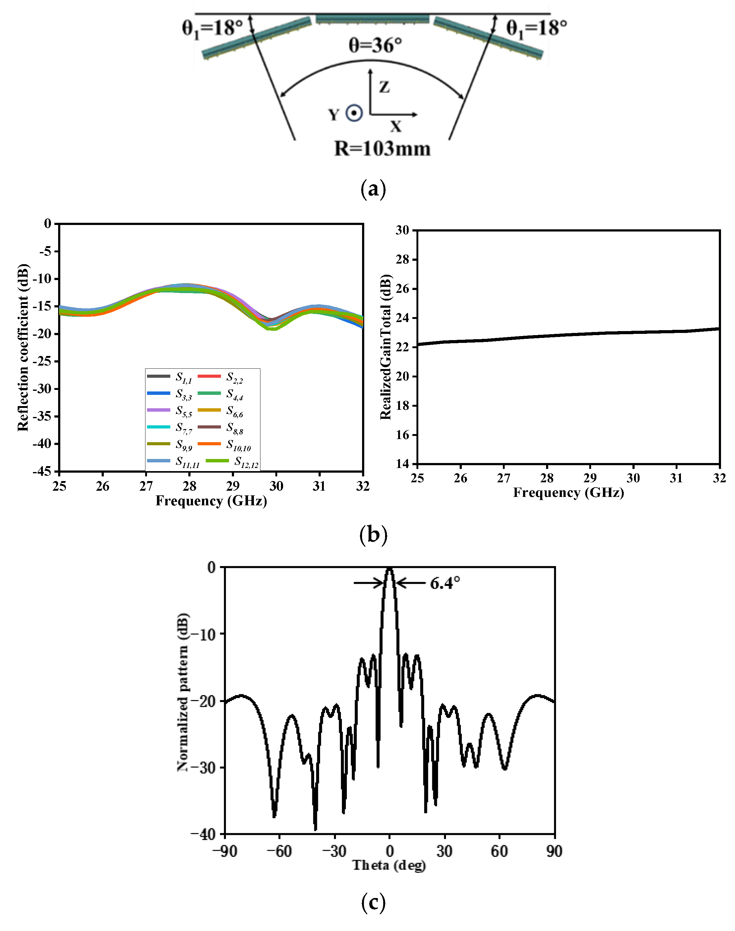
In the elevation dimension, four antenna elements are combined with equal amplitude and phase using a 1-to-4 power divider (1 dB insertion loss). Three adjacent 4 × 4 subarrays form a composite beam, with the two outer subarrays oriented at ±18° relative to the central subarray (see Figure 3a). When synthesizing a beam on the axis, the outer subarrays exhibit gain reduction. The ideal beam scanning roll-off follows a cos (θ) pattern [36], where θ represents the scan angle.
D array   =   D element + 10 log 10 ( 16 + 32 cos ( θ ) ) L wilkinson = 23.1   dB | 28.5   GHz
For Delement = 7.4 dB|28.5 GHz and θ = 18°, Delement is the directivity of the antenna element at 28.5 GHz, and the Lwilkinson exhibits a 1 dB insertion loss from the elevation 1-to-4 power divider. The 48-element phased array exhibits a directivity of 23.1 at the design frequency of 28.5 GHz.
The three planar subarrays are oriented at 36° relative to the cylinder axis (Figure 3a). Performance simulations demonstrate that S11 of the subarrays is below −13 dB across the frequency range of 26–31 GHz. The gain of the array ranges from 22.4 dB to 23.2 dB within the same frequency band (see Figure 3b). The half-power beamwidth (HPBW) on the axis is 6.4° when operating at 28.5 GHz (see Figure 3c).

2.2. Transceiver Channel Design

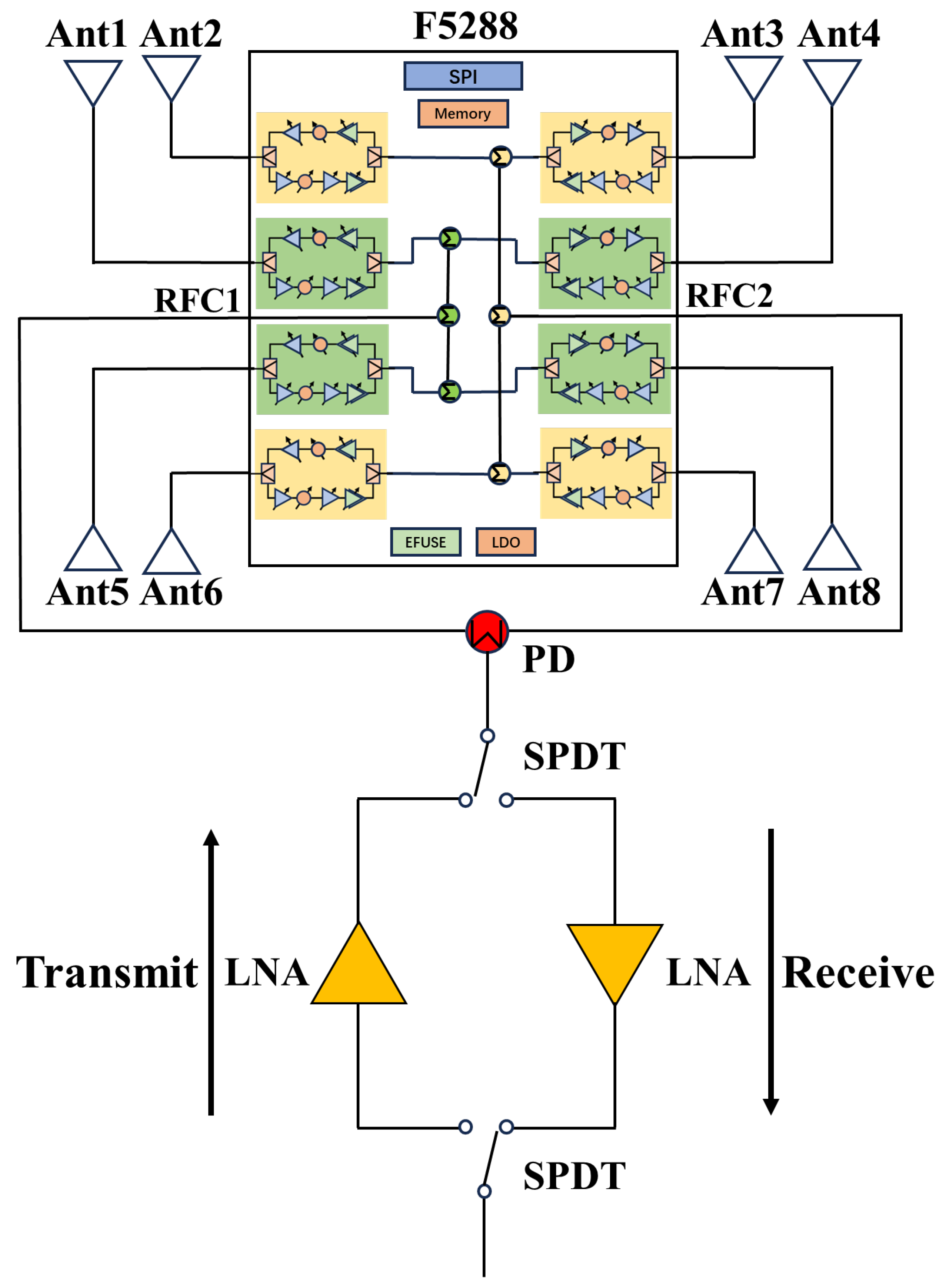
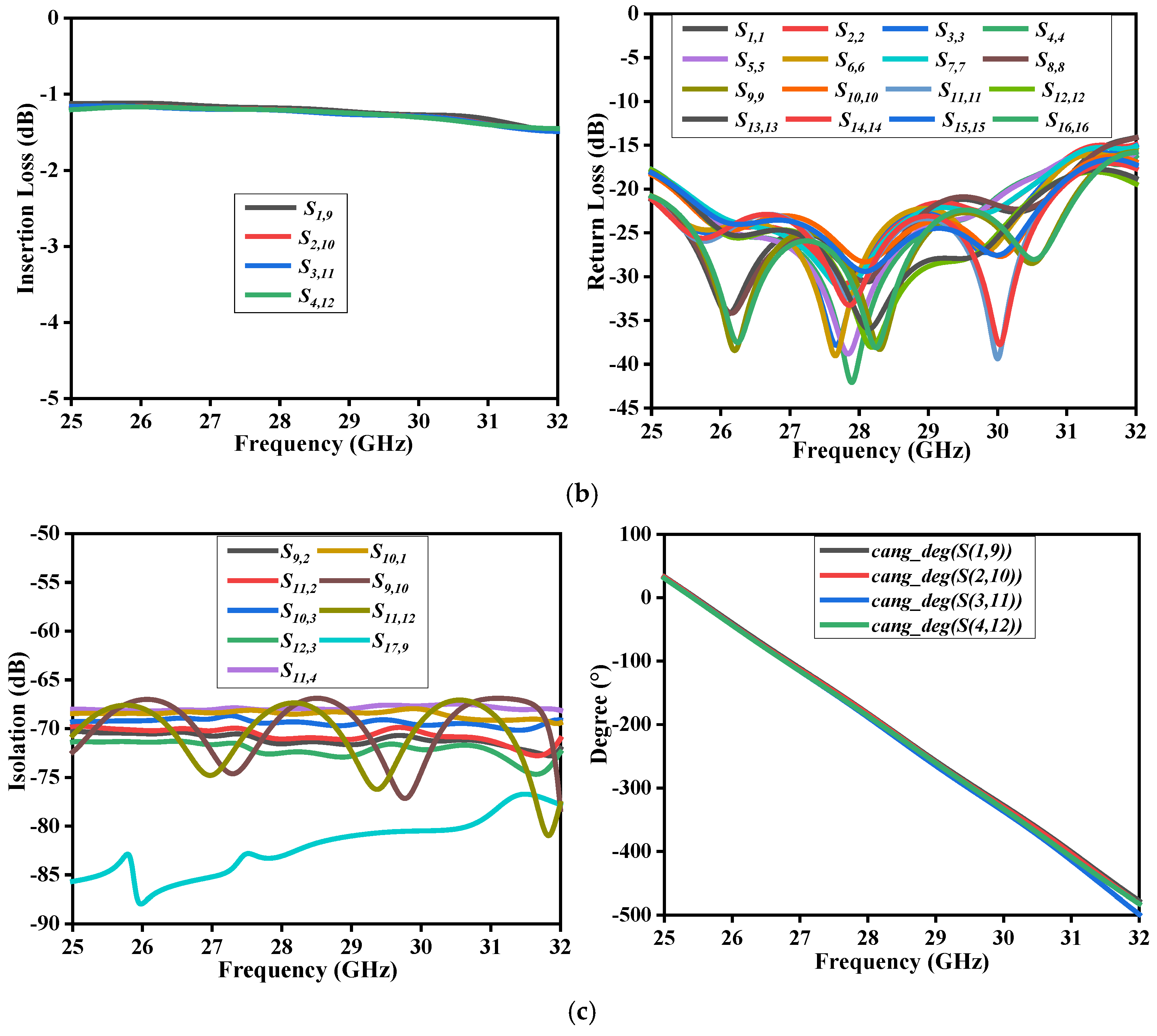
The transceiver channel comprises an F5288 8-channel SiGe BiCMOS beamforming transceiver (FCCSP package), a 1:2 ceramic power divider (PD), two ADRF5020 SPDT switches, and two QPA2628 LNAs (see Figure 4). Designed for 5G mmWave phased arrays, the F5288 operates in half-duplex mode with per-channel SPI control (see Table 1). To ensure phase–amplitude coherence between the F5288’s output and antenna feed positions, matched-length meandered transmission lines are implemented (see Figure 5a). In TX mode, the chip achieves 30.5 dB gain per channel, requiring >30.5 dB inter-channel isolation to prevent oscillation. Shielded stripline routing with grounded vias reduces coupling-induced phase–gain errors, demonstrating the following by performance simulation: 1.1–1.5 dB insertion loss, more than 16.5 dB return loss (see Figure 5b), 4° phase imbalance at 28.5 GHz, and more than 65 dB adjacent-port isolation (see Figure 5c).
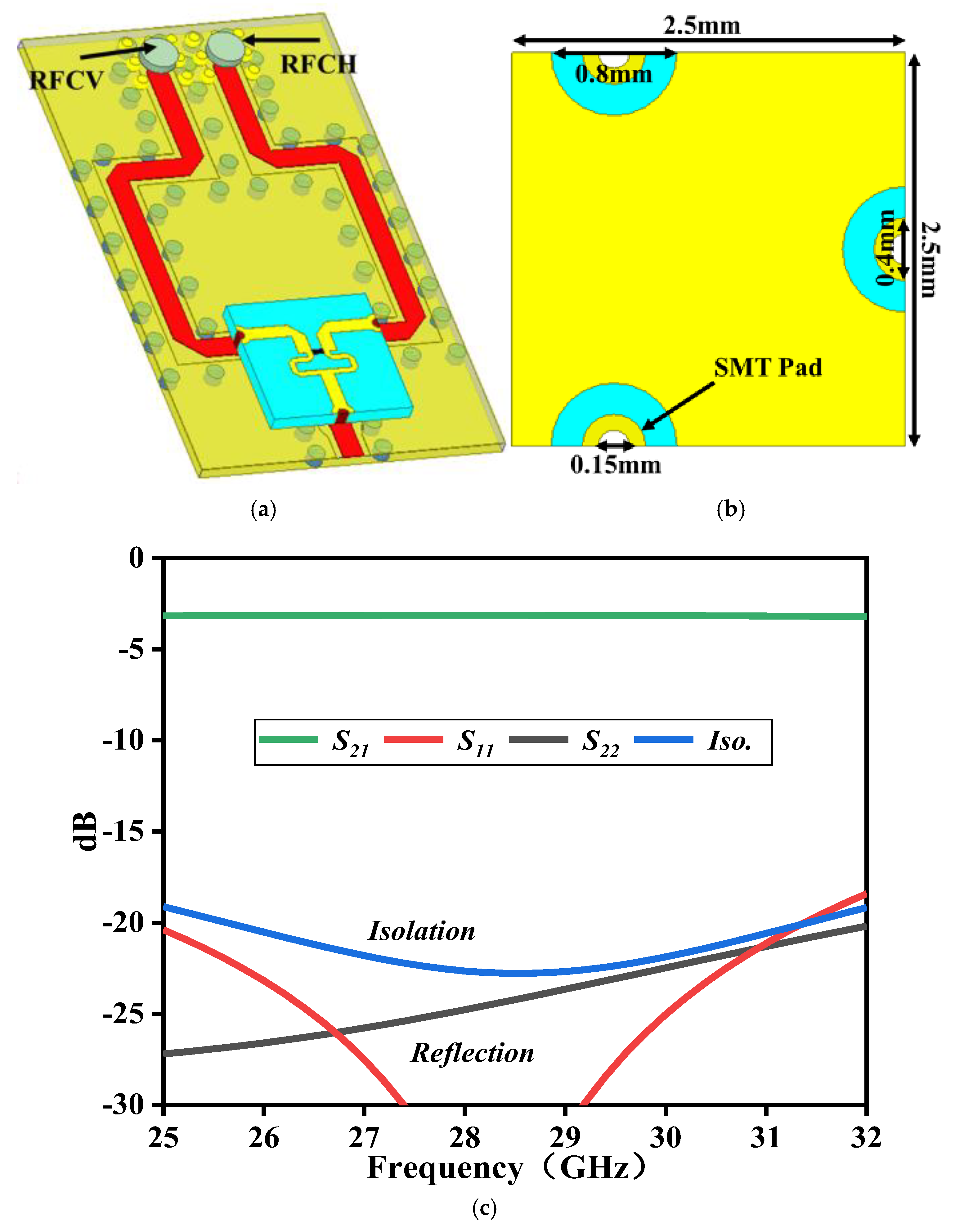
The Renesas F5288 is an 8-channel dual-polarized beamforming IC. Within this IC, four channels are combined to form each polarization port (RFCV/RFCH). These two polarization ports (RFCV and RFCH) are then combined via an external two-way power divider (as shown in Figure 6a) into a single beam port terminal. To minimize the footprint, a surface-mountable 1:2 power divider is implemented using a 0.254 mm thick Al2O3 substrate (εr = 9.9). The design features 0.15 mm diameter metallized vias centered along the microstrip edges (see Figure 6b), with 0.8 mm isolation rings and 0.4 mm landing pads at the split ports to prevent shorting. Performance simulations show 0.4 dB insertion loss, more than 19 dB return loss, and more than 20 dB isolation within the operational band (see Figure 6c).
Following the power divider, a bidirectional amplification circuit is implemented. The circuit incorporates the ADRF5020, a silicon-based single-pole double-throw (SPDT) switch with a 50-ohm absorptive design, offering low-loss transmission and high port-to-port isolation simultaneously. At 30 GHz, the loss transmission is only 2 dB, and the isolation is 60 dB. The ADRF5020 operates with a 3.5 V supply and control voltage. The QPA2628 low-noise amplifier provides 23 dB of gain with a 1.6 dB noise figure at 28.5 GHz, while consuming 315 mW from a 3.5 V supply (see Table 1).

2.3. Wilkinson Power Divider Network

To ensure phase–amplitude consistency across all 10 transceiver channels, a standard 1-to-16 power divider is employed, with unused ports terminated by 50-ohm matched loads. The power divider network is designed according to the schematic shown in Figure 7a. In the second stage of the 1-to-16 power divider, 50-ohm matching resistors are connected to the branch lines, and similarly, 50-ohm matching resistors are added to the branch lines in the third stage, ultimately forming a 1-to-10 power divider. The RF2, RF3, RF4, RF5, RF6, RF7, RF8, RF9, RF10, and RF11 signals are combined into a single RF1 output through the power divider network in Figure 7b and then routed through a single-pole double-throw (SPDT) switch to the frequency converter. The power division network is implemented using a 1:2 ceramic-based power divider, whose physical realization is shown in Figure 6b, as the fundamental unit. Coplanar waveguide (CPW) lines are designed on Layer M1 of the PCB to interconnect the power dividers. Performance simulations indicate that the power divider exhibits an insertion loss of 16.8–17.3 dB, a return loss greater than 20 dB, an isolation between ports exceeding 20 dB across 26–31 GHz, and a phase error of ±1° (see Figure 7c).

2.4. Measurement of Gain, NF, and OP1dB for the RF Beam-Control Module

The RF beam-control module in the system was tested, with the RF SSMP ports for antenna interconnection located on the side, the combined input–output RF port positioned at the center of the front panel, as shown in Figure 8a, and the power supply and control ports located on the back panel, as illustrated in Figure 8b. The measurements included the single-channel transmit–receive gain, the single-channel receiver noise figure, and the single-channel transmitter output 1 dB compression point (OP1dB).
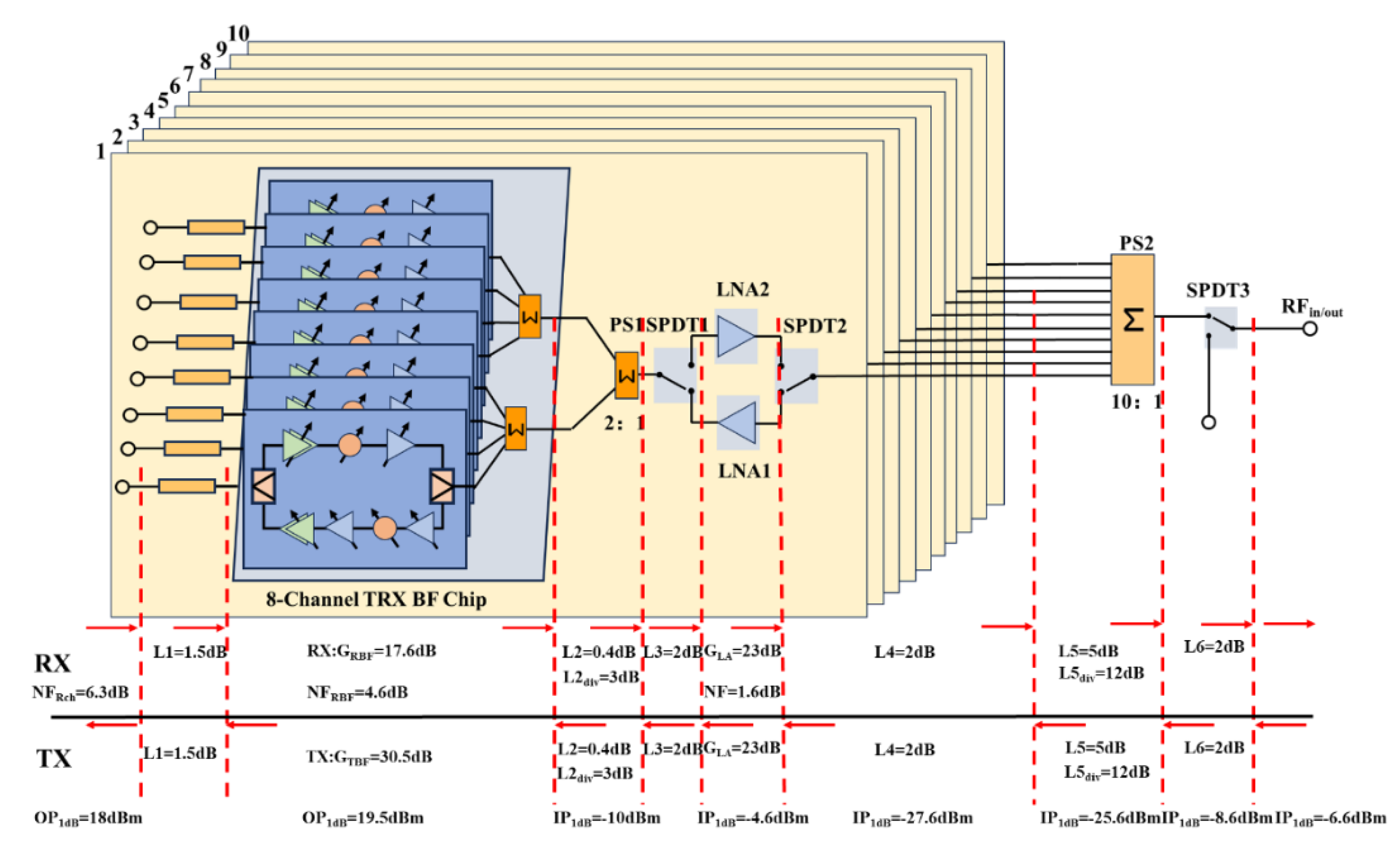
The gain GRch and noise figure (NFrec) of a single receive channel are calculated at 28.5 GHz based on the configuration shown in Figure 9.
G Rch = G RBF L 1 L 2 L 2 div L 3 + G LA L 4 L 5 L 5 div L 6   = 1.5 + 17.6 0.4 3 2 + 23 2 5 12 2 = 12.7   dB
F Rch = F L 1 + F RBF 1 G L 1 + F PS 1 1 G L 1 G RBF + F SPDT 1 1 G L 1 G RBF G PS 1 + …… = 6.3   dB
Here FRBF and GRBF are the channel NF and gain of the F5288 in receive mode. GLA is the gain of the LNA. L1, L2, L3, L2div, L4, L5, L5div, and L6 denote the losses of corresponding components in the circuit of Figure 9. FL1 and GL1 denote the NF and gain of the L1. FPS1 and GPS1 are the NF and gain of the two-way power divider. FSPDT1 is the NF of the SPDT1.
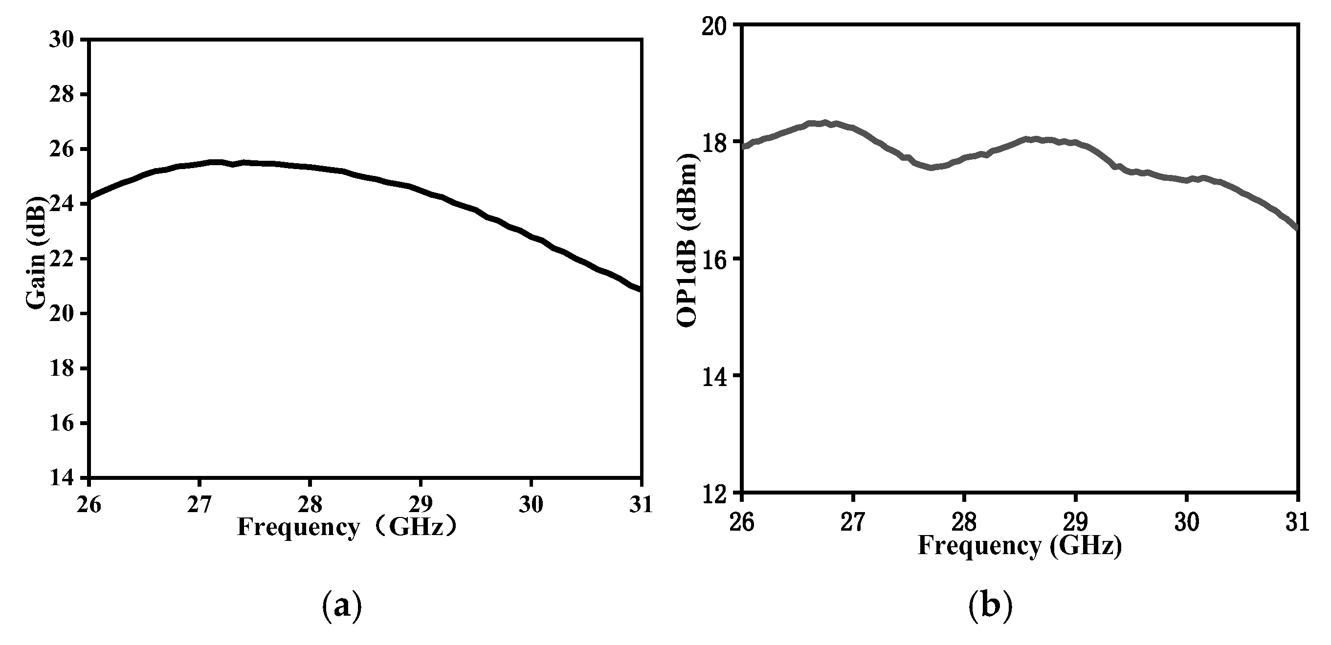
Based on the measurements, the receive gain at 28.5 GHz is 12.3 dB and the NF of 6.4 dB is achieved, in excellent agreement with theory (see Figure 10). It is well established that NF measurements include ±0.1 dB systematic error.
The gain GTch and OP1dB of a single transmit channel are calculated at 28.5 GHz based on the configuration shown in Figure 9.
G Tch = G TBF L 1 L 2 L 2 div L 3 + G LA L 4 L 5 L 5 div L 6 = 1.5 + 30.5 3.4 2 + 23 2 17 2 = 25.6   dB
where GTBF is the gain of the F5288 in transmit mode. When the input power at RFin/out is −6.6 dBm, the OP1dB of the single transmit channel at 28.5 GHz is 18 dBm (see Figure 9).
Based on the measurements, the transmit gain at 28.5 GHz is 25.1 dB and the OP1dB of 18 dBm is achieved, in excellent agreement with theory (see Figure 11).

2.5. Calculation of the Array’s G/T and EIRP

When the system operates in receive mode, a total of 12 channels of 1 × 4 array antennas simultaneously receive signals. The signals received by the 12 channels of 1 × 4 array antennas are processed through adjacent F5288 beamforming chips. One F5288 operates with all 8 channels active, while the other F5288 operates with only 4 channels active, with the remaining 4 channels powered off. The signals are then combined through two transceiver channels and a 1-to-10 power divider network and finally output through a switch. Based on the configurations illustrated in Figure 9, the calculated noise figure of the receive system is 6.1 dB.
F rec = F L 1 + F RBF 1 G L 1 + F PS 1 1 G L 1 G RBF + F SPDT 1 1 G L 1 G RBF G PS 1 + …… = 6.1   dB
The antenna array and the RF beam-control module are interconnected using KK connectors, which introduce a loss of 0.5 dB for the SSMP-KK interface within the frequency range of 26~31 GHz. Based on the calculation using Equation (5), the noise figure Frec is determined to be 6.1 dB.
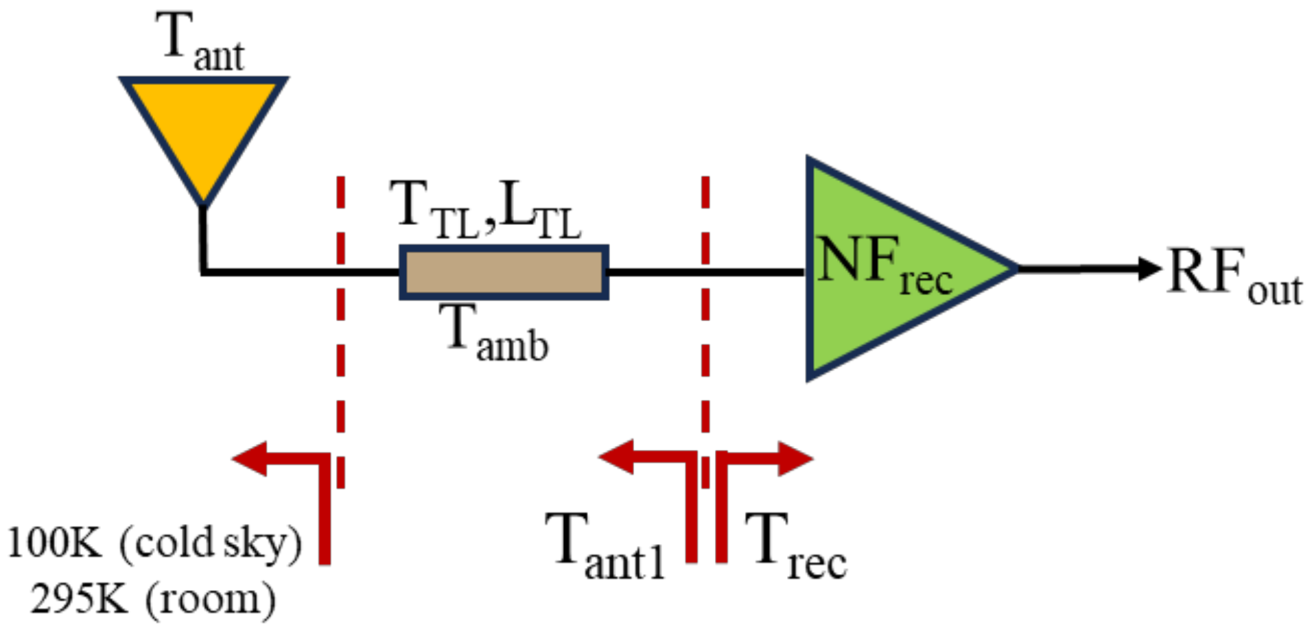
As a key figure of merit in communication systems, the G/T (gain-to-noise-temperature ratio) critically determines both the carrier-to-noise-density ratio (C/N0) and signal-to-noise ratio (SNR) in link budget analysis. The array’s G/T is evaluated under two representative conditions: (1) operational reception with cold sky observation (28.5 GHz, Tant = 100 K) and (2) anechoic chamber characterization at room temperature (Tant = 295 K) (see Figure 12).
The gain-to-noise-temperature ratio (G/T) is mathematically expressed as
G / T = G ant 10 log 10 ( T s )
where Gant represents the array antenna gain, which includes the combined gain of the array antenna before the LNA, the synthesis loss of the four-element antenna, the feed loss LTL, the power divider synthesis loss Lsyn, and the beam scanning loss cos (θ).
G ant   = 10 log 10 16 + 32 cos θ + D ant L TL L syn
where Dant represents the directivity of an individual antenna element, determined by its unit cell aperture area. For example, at the operational frequency of 28.5 GHz, the array gain Gant is derived as
G ant = 10 log 10 16 + 32 cos θ + D ant L TL L syn = 10 log 10 46.43 + 7.4 0.5 1 = 22.6   dB
The system noise temperature (Ts) comprises three principal components: the antenna noise temperature (Tant), the transmission line thermal noise contribution (TTL), and the receiver equivalent input noise temperature (Trec), expressed as
T s = T ant 1 + T rec
T ant 1 = T ant / L TL + T TL
T rec = T 0 ( F rec 1 )
T TL = T amb 1 1 / L TL
where T0 = 290 K denotes the standardized noise reference temperature for noise figure characterization and Tamb = 295 K represents the measured ambient temperature of the transmission line assembly. Substituting all values into Equations (9)–(12), the system noise temperature Ts for Tant = 100 K is calculated as
T s = T ant / L TL + T TL + T rec = 100 ( 10 0.5 / 10 ) + 295 1 10 0.5 / 10 + 290 10 0.61 1 = 89.1266 + 32.155 + 891.4 = 1012.68   K
Substituting Equations (8) and (13) into Equation (6), the G/T for Tant = 100 K is
G / T = 22.6 10 log 10 1012.68 = 22.6 30.05 = 7.45   dB / K
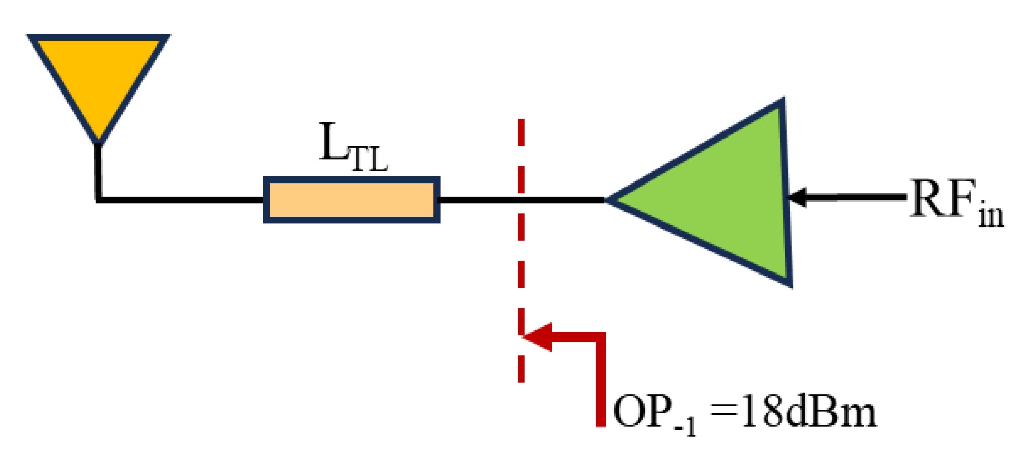
In the transmit state, the equivalent isotropically radiated power (EIRP) of the array on axis is calculated (see Figure 13).
When the beamforming chip operates at its OP1dB, the array’s EIRP is derived as
EIR P 1 dB   = 10 log 10 ( 16 + 32 cos θ ) + D ant + 10 log 10 12 + P elem L TL L syn = 16.7 + 7.4 + 10.8 + 18 0.5 1 = 51.4   dBm
where Pelem is the 1 dB compression point of the channel output.

3. Measurement Results

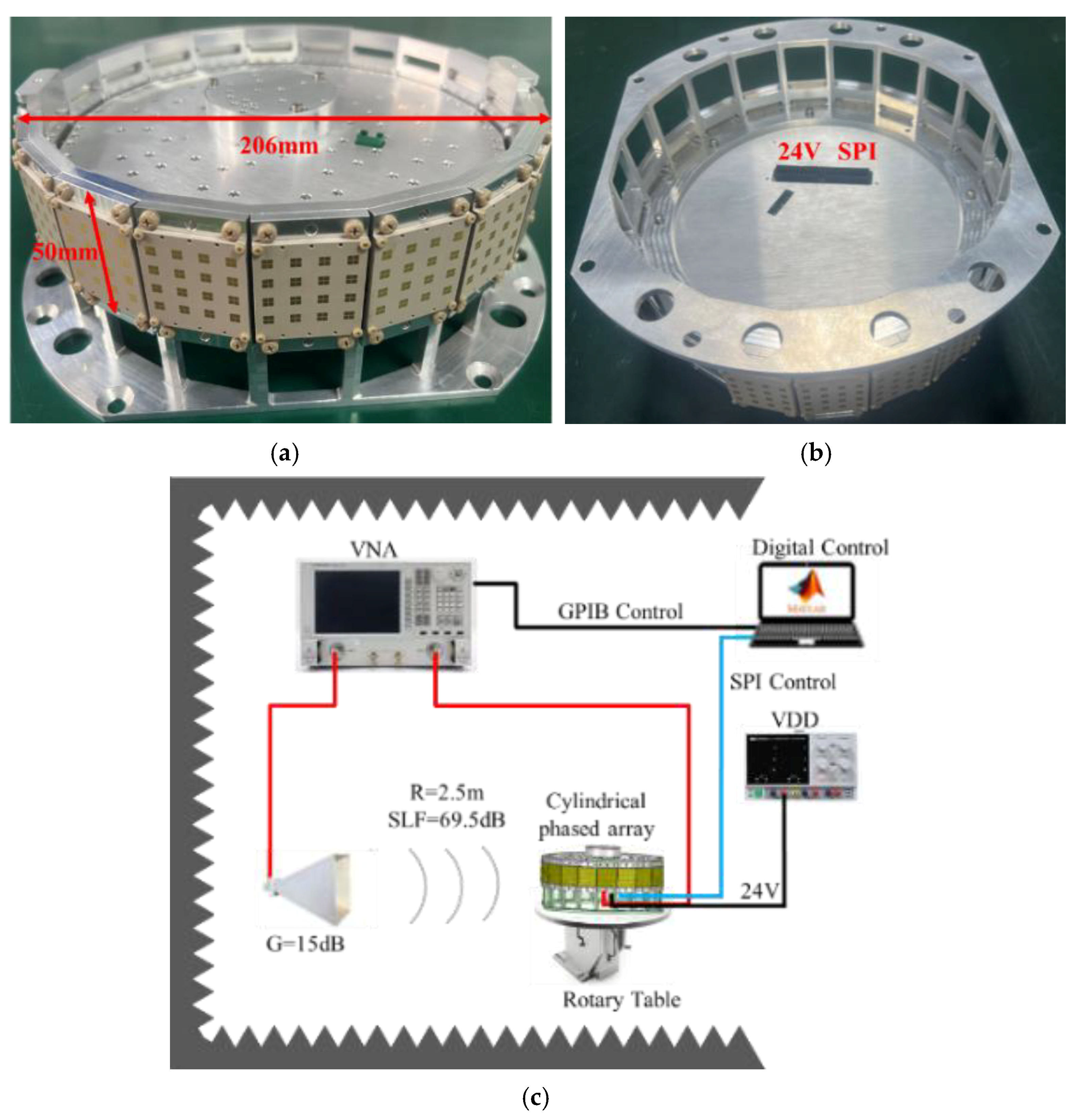
The CCTAPA characterization was performed in an RF-shielded anechoic chamber using a Keysight N5245A vector network analyzer (Santa Rosa, CA, USA) and a traceable Ka-band standard-gain horn antenna, with full measurement calibration. Since only 48 element antennas are active at a time, arranged in a 4 × 12 configuration, the far-field distance at 28.5 GHz was calculated using the far-field formula, yielding a theoretical distance of 0.45 m (see Figure 14c). However, the actual measurement distance was set to 2.5 m to ensure accurate far-field conditions.
RFF ,   48 = 2 ( L   ×   W ) λ = 0.45   m   |   28.5   GHz
Here, L represents the length of the 4 × 12 array antenna, and W denotes its width. To eliminate additional quadrature phase errors, the beam is focused onto the horn antenna, and measurements are conducted in the radiating far-field. Since only three subarrays are active at a time, the entire array system determines which beamforming chips are operational based on the actual working antenna array positions. This approach is designed to reduce overall power consumption and minimize thermal management challenges. The FPGA is used to identify which beamforming chips should be active, while the non-operational chips are powered off. According to the application requirements, one-and-a-half beamforming chips are active simultaneously, with the beamforming chips consuming the most power in the transmit state. Each BF chip consumes 5.4 W in the transmit state, resulting in a total power dissipation of 8.1 W for the equivalent of 1.5 BF chips. During operation, heat generated by the beamforming chips is conducted to the RF beam-control module housing, which then transfers the heat to the system installation frame. Two internal fans are used to dissipate the heat, maintaining the array’s operating temperature at 35 ± 5 °C.

3.1. Calibration

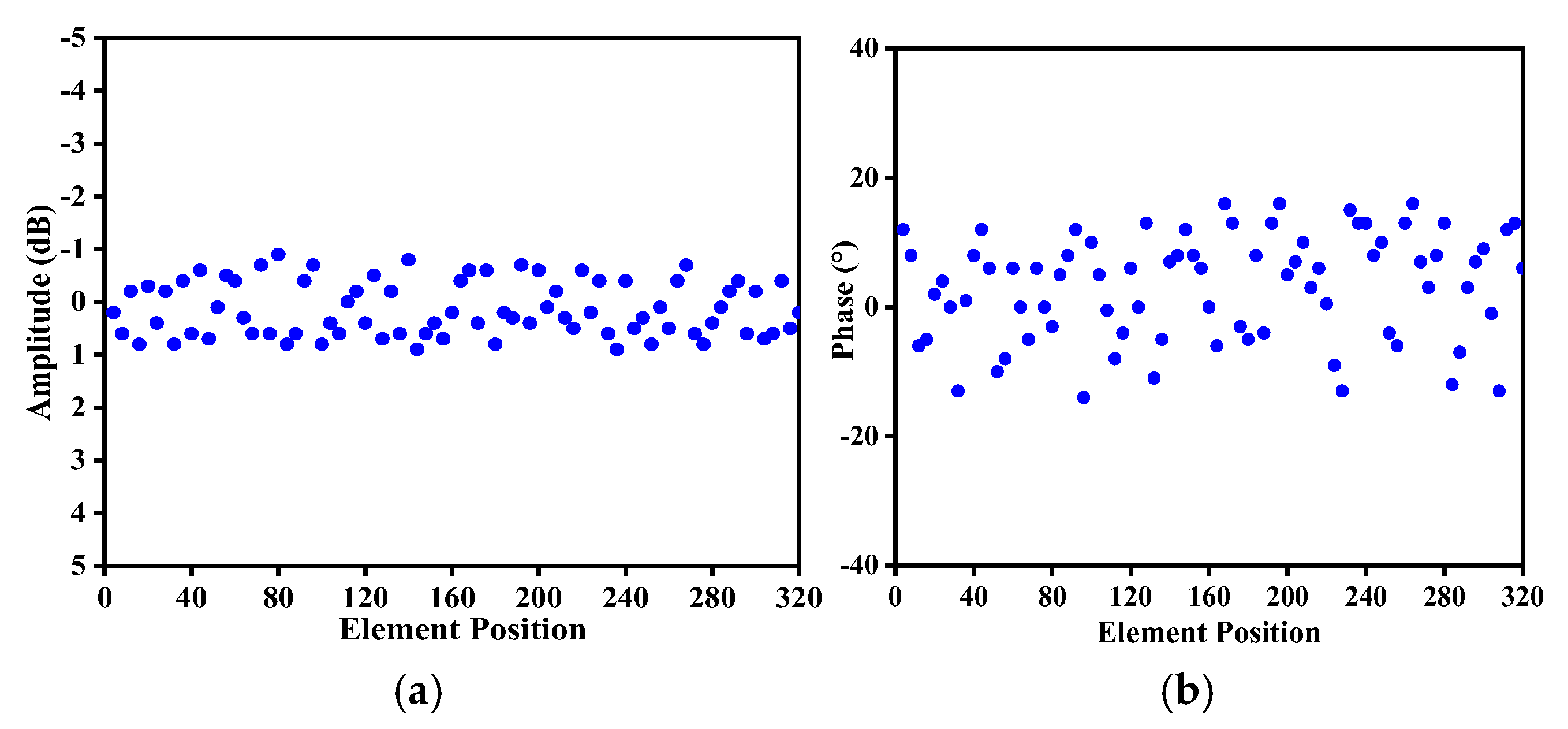
Near-field probe calibration is implemented to precisely align the amplitude and phase responses across all antenna array channels. Since each column of four antenna elements is combined with equal amplitude and phase, the central element of the four-unit column is selected for near-field testing to determine its amplitude and phase characteristics. Calibration is then performed based on these measurements. By activating only one channel of the 8-channel beamforming chip at a time, the received signal S21 at the phased-array antenna from the horn antenna is recorded. The near-field test provides the radiation amplitude and phase values of the array elements. The characterized amplitude and phase variations are stored in a dedicated calibration lookup table for real-time beamforming adjustment. The antenna control system compensates for the phase differences in real time using the phase shifters of the corresponding transmit or receive channels, while the amplitude errors are corrected by adjusting the variable gain amplifiers (VGAs) in the corresponding beamforming chips. This pre-compensation ensures that each element achieves the desired amplitude and phase response during operation. Calibration is performed at the frequency of 28.5 GHz. Figure 15 displays the post-calibration amplitude and phase error distributions, respectively, demonstrating the effectiveness of the compensation algorithm. During the calibration process, the X-axis in Figure 15 represents the positional range of the array antenna elements. As four antennas form one cluster corresponding to a single set of calibration data and position, a total of 80 amplitude calibration data points and 80 phase calibration data points are distributed across the starting positions of the array antennas, as illustrated in Figure 15. The array channels exhibit an amplitude error of 0.53 dB RMS and a phase error of 12.34° RMS.

3.2. Frequency Response

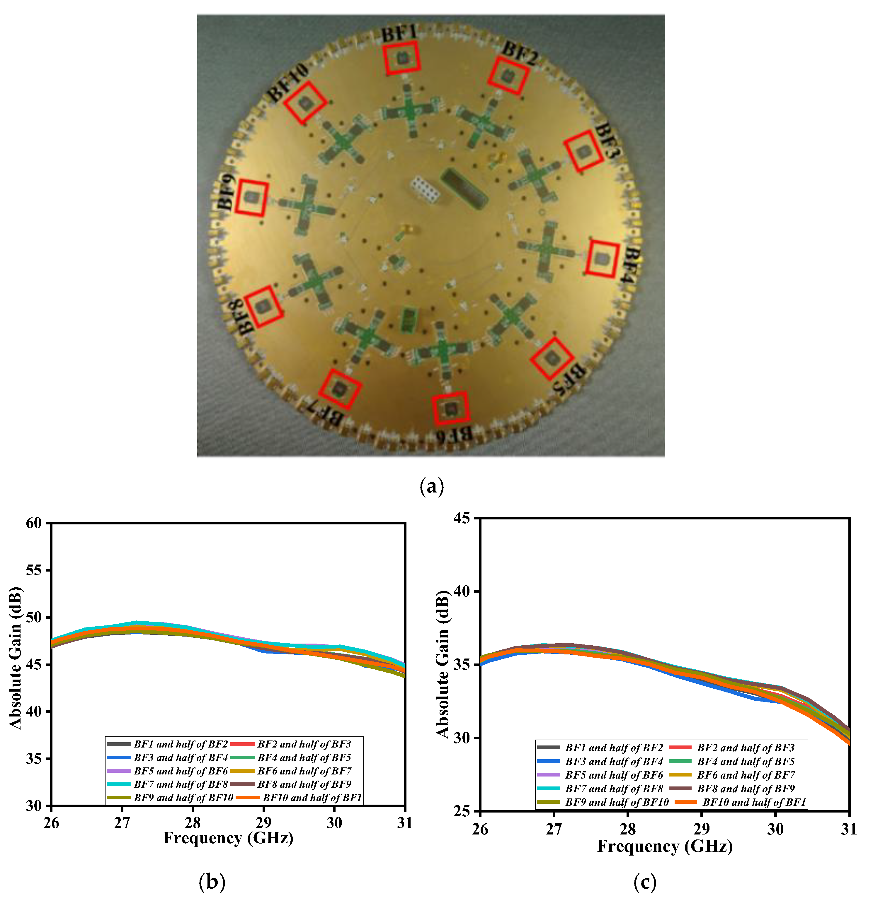
As illustrated in Figure 16, the S21 measurement methodology normalizes both the standard-gain horn characteristics and wave propagation losses in the anechoic environment. The ten beamforming chips in the RF beam-control module are labeled as BF1 to BF10. Each beam synthesis involving three subarrays requires the activation of one-and-a-half adjacent beamforming chips. Therefore, to achieve 360° scanning with the 320-element cylindrical array antenna, the beamforming chips are activated in 20 steps. Ten specific combinations of beamforming chips are selected for excitation, as detailed in the accompanying Table 2. The corresponding beams are excited accordingly.
The test results indicate that the array’s transmit gain at 28.5 GHz ranges from 48.2 dB to 48.7 dB, while the receive gain ranges from 35.3 dB to 35.8 dB (see Figure 16). The measurements align well with the simulation results, with minor discrepancies attributed to variations between chips, antenna assembly tolerances, and design imperfections.

3.3. Far-Field Radiation Characteristics of the CCTAPA

Utilizing the symmetry of the chip and antenna layout, the antenna array associated with beamforming chips BF1 and half of BF2 in transmission mode (see Figure 16a) was chosen for testing. Figure 17 compares measured and simulated azimuth-plane normalized radiation patterns at 26, 28.5, and 31 GHz. A high degree of agreement is observed between the measured and simulated radiation patterns. From Figure 17, it is observed that when the array scans to ±9°, the gain decreases by 0.6 dB at 26 GHz, 0.3 dB at 28.5 GHz, and 0.5 dB at 31 GHz. Since the calibration data at 28.5 GHz was used during testing, the gain reduction at 26 GHz and 31 GHz is slightly more pronounced compared to that at 28.5 GHz. Figure 18 illustrates the comparison between measured and simulated radiation patterns in the elevation plane at 26 GHz, 28.5 GHz, and 31 GHz. As shown in Figure 18, the measured and simulated radiation patterns demonstrate good consistency at 26 GHz, 28.5 GHz, and 31 GHz in the elevation plane. At 26 GHz, the beamwidth is 21°; at 28.5 GHz, it is 20°; and at 31 GHz, it narrows to 17.5°.
Beams 1 through 10, as illustrated in Figure 19, correspond to the beam identifiers listed in Table 2. By controlling and switching the beamforming chips as outlined in Table 2, the array achieves 360° beam scanning. The test data in Figure 19 indicate that at 28.5 GHz, each beam on the axis exhibits a gain fluctuation of 0.5 dB during 360° scanning. Based on the analysis of the test results in Figure 17b, each beam experiences a gain reduction of 0.3 dB when scanning within a ±9° range at 28.5 GHz. Combining these observations, the array demonstrates a gain fluctuation of 0.8 dB loss during 360° scanning at 28.5 GHz. This performance significantly surpasses the scanning gain loss typically observed in planar phased arrays.

3.4. Measurement Results of Antenna Array G/T

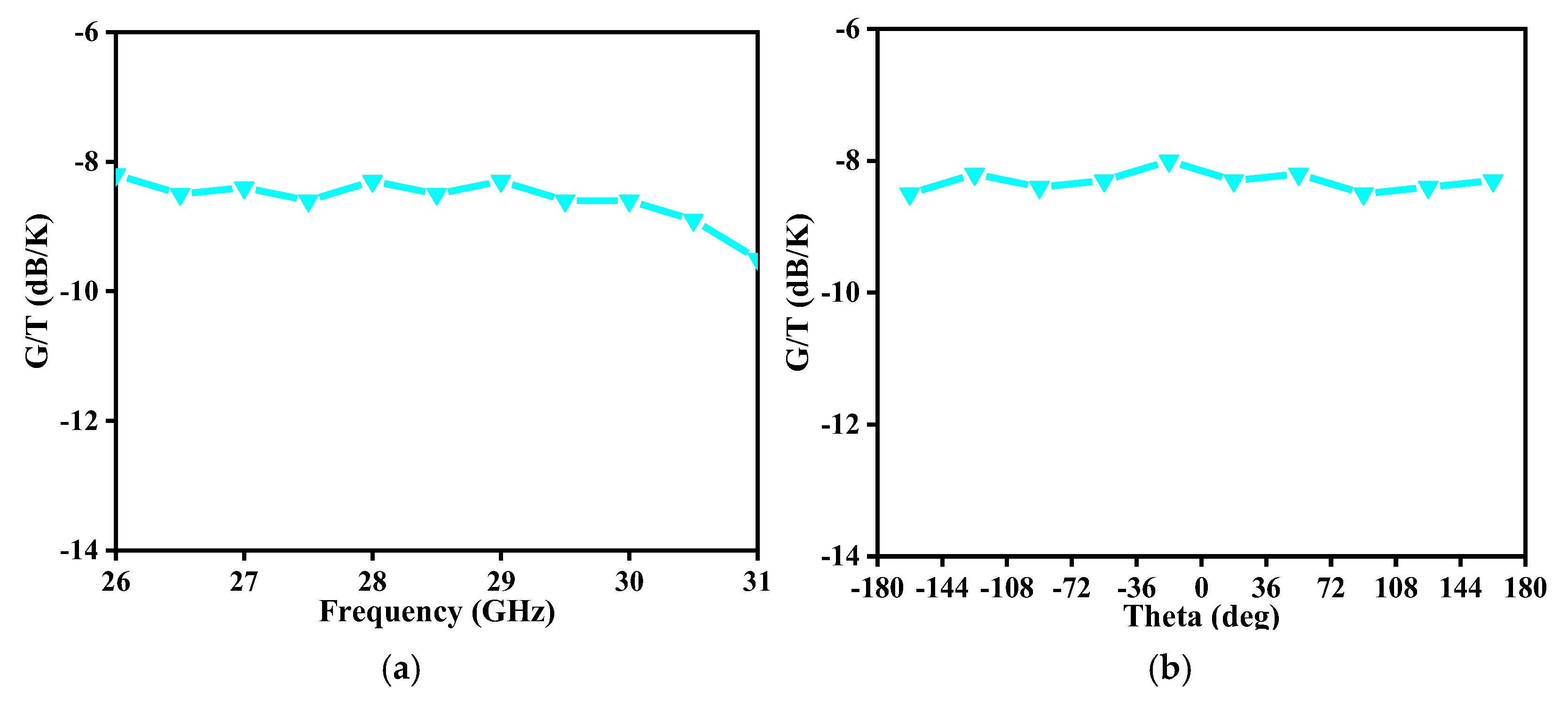
In the receive state, the CCTAPA is divided into 10 beams for G/T measurement, as outlined in Table 2. The G/T of Beam 1 is measured in the axis direction across different frequencies. At 28.5 GHz, the theoretical G/T of the array is calculated to be −7.45 dB/K. As shown in Figure 20a, the measured G/T at 28.5 GHz is −8.5 dB/K, which aligns well with the theoretical prediction. It is widely recognized that deterioration in G/T results from both antenna gain synthesis loss and elevated feed system losses.
The noise figure of the beamforming chip degrades with increasing frequency, and the measured trend in Figure 20a matches the theoretical expectation. From the measurements in Figure 20b, the G/T of the 10 beams on the axis during 360° scanning at 28.5 GHz fluctuate between −8 dB/K and −8.5 dB/K.

3.5. Measurement Results of Antenna Array EIRP

Figure 21a presents the measured EIRP of Beam 1 on the axis across different frequencies. At 28.5 GHz, the theoretical EIRP of the array is calculated to be 51.4 dBm, while the measured EIRP is 51 dBm, showing good agreement. The OP1dB of the beamforming chip remains relatively stable with increasing frequency, and the test results align well with the theoretical predictions. As demonstrated in Figure 21b, the EIRP of the 10 beams on axis during 360° scanning at 28.5 GHz range from 50.6 dBm to 51.3 dBm.

4. Discussion

Table 3 presents a performance comparison between the proposed 320-element linearly polarized 1D CCTAPA and other state-of-the-art phased-array antennas. This work presents a CCTAPA achieving superior performance: 360° scanning capability, merely 0.8 dB gain fluctuation, and ultra-low power consumption of 0.027 W per element. To the best of our knowledge, this represents the first reported Ka-band CCTAPA simultaneously achieving full-azimuth coverage, minimal gain fluctuation, and the lowest per-element power consumption. In summary, the proposed CCTAPA represents an advanced solution for aerial platforms, satellite communications, and 5G millimeter-wave base stations, offering full 360° coverage, low gain fluctuation, low cost, and low power consumption.

5. Conclusions

A Ka-band cylindrical conformal transceiver active phased array capable of 360° azimuth scanning featuring low gain fluctuation, low power consumption, and low cost is first introduced in this paper. The phased array achieves full-azimuth scanning through electronic beam steering within ±9° using three adjacent subarrays, combined with time-sequential switching of 20 beams in different azimuths. This time-multiplexed beam-switching architecture enables low-power operation. Fabricated prototypes demonstrate excellent performance across 26–31 GHz, exhibiting merely 0.8 dB gain variation during full-azimuth scanning at 28.5 GHz. Both azimuth and elevation radiation patterns show good agreement between simulations and measurements, as do the EIRP and G/T. The system maintains tight assembly tolerances, and its performance advantages make it particularly suitable for airborne platform integration.

Author Contributions

Conceptualization, W.L. and W.C.; methodology, W.L. and W.C.; validation, W.L.; formal analysis, W.L.; investigation, W.L.; data curation, W.L.; writing, W.L.; review and editing, S.Z., A.Z. and W.C. All authors have read and agreed to the published version of the manuscript.

Funding

This research received no external funding.

Institutional Review Board Statement

Not applicable.

Informed Consent Statement

Not applicable.

Data Availability Statement

The original contributions presented in this study are included in the article. Further inquiries can be directed to the corresponding author.

Conflicts of Interest

The authors declare no conflicts of interest.

References

  1. Xiao, Z.; Han, Z.; Nallanathan, A.; Dobre, O.A.; Clerckx, B.; Choi, J.; He, C.; Tong, W. Antenna Array Enabled Space/Air/Ground Communications and Networking for 6G. IEEE J. Sel. Areas Commun. 2022, 40, 2773–2804. [Google Scholar] [CrossRef]
  2. Jia, Z.; Sheng, M.; Li, J.; Niyato, D.; Han, Z. LEO-satellite-assisted UAV: Joint trajectory and data collection for Internet of remote things in 6G aerial access networks. IEEE Internet Things J. 2021, 8, 9814–9826. [Google Scholar] [CrossRef]
  3. Fang, X.; Feng, W.; Wang, Y.; Chen, Y.; Ge, N.; Ding, Z.; Zhu, H. NOMA-based hybrid satellite-UAV-terrestrial networks for 6G maritime coverage. IEEE Trans. Wirel. Commun. 2023, 22, 138–152. [Google Scholar] [CrossRef]
  4. Ghamari, M.; Rangel, P.; Mehrubeoglu, M.; Tewolde, G.S.; Sherratt, R.S. Unmanned aerial vehicle communications for civil applications: A review. IEEE Access. 2022, 10, 102492–102531. [Google Scholar] [CrossRef]
  5. Han, R.; Bai, L.; Wen, Y.; Liu, J.; Choi, J.; Zhang, W. UAV-aided backscatter communications: Performance analysis and trajectory optimization. IEEE J. Sel. Areas Commun. 2021, 39, 3129–3143. [Google Scholar] [CrossRef]
  6. Li, K.-X.; Guo, Z.-J.; Hao, Z.-C. A Multipolarized Planar Phased Array for LEO SATCOM Applications. IEEE Antennas Wirel. Propag. Lett. 2022, 21, 2273–2277. [Google Scholar] [CrossRef]
  7. Wei, C.Y. A dual circularly polarized SIW-fed phased array antenna with wide-angle beam scanning range. IEEE Trans. Antennas Propag. 2022, 70, 7393–7402. [Google Scholar] [CrossRef]
  8. Kim, D.; Hwang, M.; Kim, G.; Kim, S. Self-Deployable Circularly Polarized Phased Yagi–Uda Antenna Array Using 3-D Printing Technology for CubeSat Applications. IEEE Antennas Wirel. Propag. Lett. 2022, 21, 2249–2253. [Google Scholar] [CrossRef]
  9. Das, S.; Sharma, S.K.; Waldstein, S.W.; Downey, J.M.; Schoenholz, B.L.; Dever, S.M.; Nessel, J.A.; Banerjee, R. A Flat-Panel 8 × 8 Wideband K-/Ka-Band Dual Circularly Polarized Phased Array Antenna for CubeSat Communications. IEEE Trans. Antennas Propag. 2023, 71, 4153–4166. [Google Scholar] [CrossRef]
  10. Yan, T.-Y.; Ding, X.-H.; Yang, J.-Y.; Chen, J.-X. A Low-Cost Compact Dual-Polarized Patch Antenna Array for 5G Massive MIMO Base Station. IEEE Antennas Wirel. Propag. Lett. 2024, 23, 1381–1385. [Google Scholar] [CrossRef]
  11. Chieh, J.-C.S.; Yeo, E.; Farkouh, R.; Castro, A.; Kerber, M.; Olsen, R.B.; Merulla, E.J.; Sharma, S.K. Development of flat panel active phased array antennas using 5G silicon RFICs at Ku- and Ka-bands. IEEE Access 2020, 8, 192669–192681. [Google Scholar] [CrossRef]
  12. Liu, H.; Qing, A.; Xu, Z.; Yu, Z.; Zhang, S. Design of physically connected wideband SIW cavity-backed patch antenna for wide-angle scanning phased arrays. IEEE Antennas Wirel. Propag. Lett. 2021, 20, 406–410. [Google Scholar] [CrossRef]
  13. Mailloux, R.J. Phased Array Antenna Handbook, 3rd ed.; Artech House: Norwood, MA, USA, 2017; pp. 235–508. [Google Scholar]
  14. Low, K.K.W.; Nafe, A.; Zihir, S.; Kanar, T.; Rebeiz, G.M. A scalable circularly-polarized 256-element Ka-band phased-array SATCOM transmitter with ±60° beam scanning and 34.5 dBW EIRP. In Proceedings of the 2019 IEEE MTT-S International Microwave Symposium, Boston, MA, USA, 2–7 June 2019; pp. 1064–1067. [Google Scholar]
  15. Low, K.K.W.; Zihir, S.; Kanar, T.; Rebeiz, G.M. A Scalable Switchable Dual-Polarized 256-Element Ka-Band SATCOM Transmit Phased-Array with Embedded RF Driver and ±70◦ beam scanning. In Proceedings of the 2020 IEEE/MTT-S International Microwave Symposium, Los Angeles, CA, USA, 4–6 August 2020; pp. 821–824. [Google Scholar]
  16. Nafe, A.; Sayginer, M.; Kibaroglu, K.; Rebeiz, G.M. 2×64 dual-polarized dual-beam single-aperture 28 GHz phased array with high cross-polarization rejection for 5G polarization MIMO. In Proceedings of the 2019 IEEE MTT-S International Microwave Symposium, Boston, MA, USA, 2–7 June 2019; pp. 484–487. [Google Scholar]
  17. Nafe, A.; Sayginer, M.; Kibaroglu, K.; Rebeiz, G.M. 2×64-element dual-polarized dual-beam single-aperture 28-GHz phased array with 2×30 Gb/s links for 5G polarization MIMO. IEEE Trans. Microw. Theory Tech. 2020, 68, 3872–3884. [Google Scholar] [CrossRef]
  18. Lin, H.S.; Cheng, Y.J. A tiling method for sub-arrayed spherical conformal phased array antennas based on maximum 3-D space entropy model. IEEE Trans. Antennas Propag. 2024, 72, 2513–2523. [Google Scholar] [CrossRef]
  19. Sengupta, D.; Smith, T.; Larson, R. Radiation characteristics of a spherical array of circularly polarized elements. IRE Trans. Antennas Propag. 1968, 16, 2–7. [Google Scholar] [CrossRef]
  20. Rao, V.S.; Srinivasan, V.V.; Pal, S. Generation of dual beams from spherical phased array antenna. Electron. Lett. 2009, 45, 441–442. [Google Scholar] [CrossRef]
  21. Braaten, B.D.; Roy, S.; Irfanullah, I.; Nariyal, S.; Anagnostou, D.E. Phase-compensated conformal antennas for changing spherical surfaces. IEEE Trans. Antennas Propag. 2014, 62, 1880–1887. [Google Scholar] [CrossRef]
  22. Hizal, A. Wide angle scanning conformal phased array on a spherical surface. In Proceedings of the 2013 IEEE International Symposium on Phased Array Systems and Technology, Waltham, MA, USA, 15–18 October 2013; pp. 259–266. [Google Scholar]
  23. Srinivasan, V.V.; Kumar, C.; Kumar, B.P.; Lakshmeesha, V.K.; Pal, S. Design considerations for dual circularly polarized spherical phased array antenna at X-band for spacecraft data transmission. In Proceedings of the 2011 IEEE Applied Electromagnetics Conference (AEMC), Kolkata, India, 18–22 December 2011; pp. 1–4. [Google Scholar]
  24. Wu, Y.F.; Cheng, Y.J. Spherical conformal antenna array based on 3D printing framework. In Proceedings of the 2016 IEEE MTT-S International Microwave Workshop Series on Advanced Materials and Processes for RF and THz Applications, Chengdu, China, 20–22 July 2016; pp. 1–2. [Google Scholar]
  25. Kumar, C.; Kumar, B.P.; Kumar, V.S.; Srinivasan, V.V. Dual circularly polarized spherical phased-array antenna for spacecraft application. IEEE Trans. Antennas Propag. 2013, 61, 598–605. [Google Scholar] [CrossRef]
  26. Oraizi, H.; Soleimani, H. Optimum pattern synthesis of non-uniform spherical arrays using the Euler rotation. IET Microw. Antennas Propag. 2015, 9, 898–904. [Google Scholar] [CrossRef]
  27. Josefsson, L.; Persson, P. Conformal Array Antenna Theory and Design; Wiley-IEEE Press: Hoboken, NJ, USA, 2006; pp. 49–70. [Google Scholar]
  28. Gan, T.H.; Liu, A.; Tan, P.K.; Lu, J. A bendable wideband dual-polarization conformal phased-array antenna. IEEE Antennas Wirel. Propag. Lett. 2023, 22, 1952–1956. [Google Scholar] [CrossRef]
  29. Hussain, S.; Qu, S.W.; Zhang, P.; Wang, X.H.; Yang, S. A low-profile, wide-scan, cylindrically conformal X-band phased array. IEEE Antennas Wirel. Propag. Lett. 2021, 20, 1503–1507. [Google Scholar] [CrossRef]
  30. Gao, Y.; Jiang, W.; Hu, W.; Wang, Q.; Zhang, W.; Gong, S. A dual-polarized 2-D monopulse antenna array for conical conformal applications. IEEE Trans. Antennas Propag. 2021, 69, 5479–5488. [Google Scholar] [CrossRef]
  31. Li, A.; Qu, S.W.; Yang, S. Conformal array antenna for applications in wide-scanning phased array antenna systems. IEEE Antennas Wirel. Propag. Lett. 2022, 21, 1762–1766. [Google Scholar] [CrossRef]
  32. Jamal, H.A.; Hu, C.; Kwao, E.; Zeng, K.; Tentzeris, M.M. Toward 5G/mm-wave shape-changing origami-inspired phased arrays for near-limitless arbitrarily reconfigurable radiation patterns: Realiza tion, actuation, and calibration. IEEE Trans. Microw. Theory Techn. 2025, 73, 397–411. [Google Scholar] [CrossRef]
  33. You, D. A Ka-band 64-element deployable active phased-array TX on a flexible hetero segmented liquid crystal polymer for small satellites. IEEE Microw. Wireless Technol. Lett. 2023, 33, 903–906. [Google Scholar] [CrossRef]
  34. Peng, J.-J.; Qu, S.-W.; Xia, M.; Yang, S. Conformal phased array antenna for unmanned aerial vehicle with ±70 scanning range. IEEE Trans. Antennas Propag. 2021, 69, 4580–4587. [Google Scholar] [CrossRef]
  35. Pozar, D.M. Microstrip antennas. Proc. IEEE 1992, 80, 79–91. [Google Scholar] [CrossRef]
  36. Visser, H.J. Array and Phased Array Antenna Basics; Wiley: Hoboken, NJ, USA, 2006; pp. 244–267. [Google Scholar]
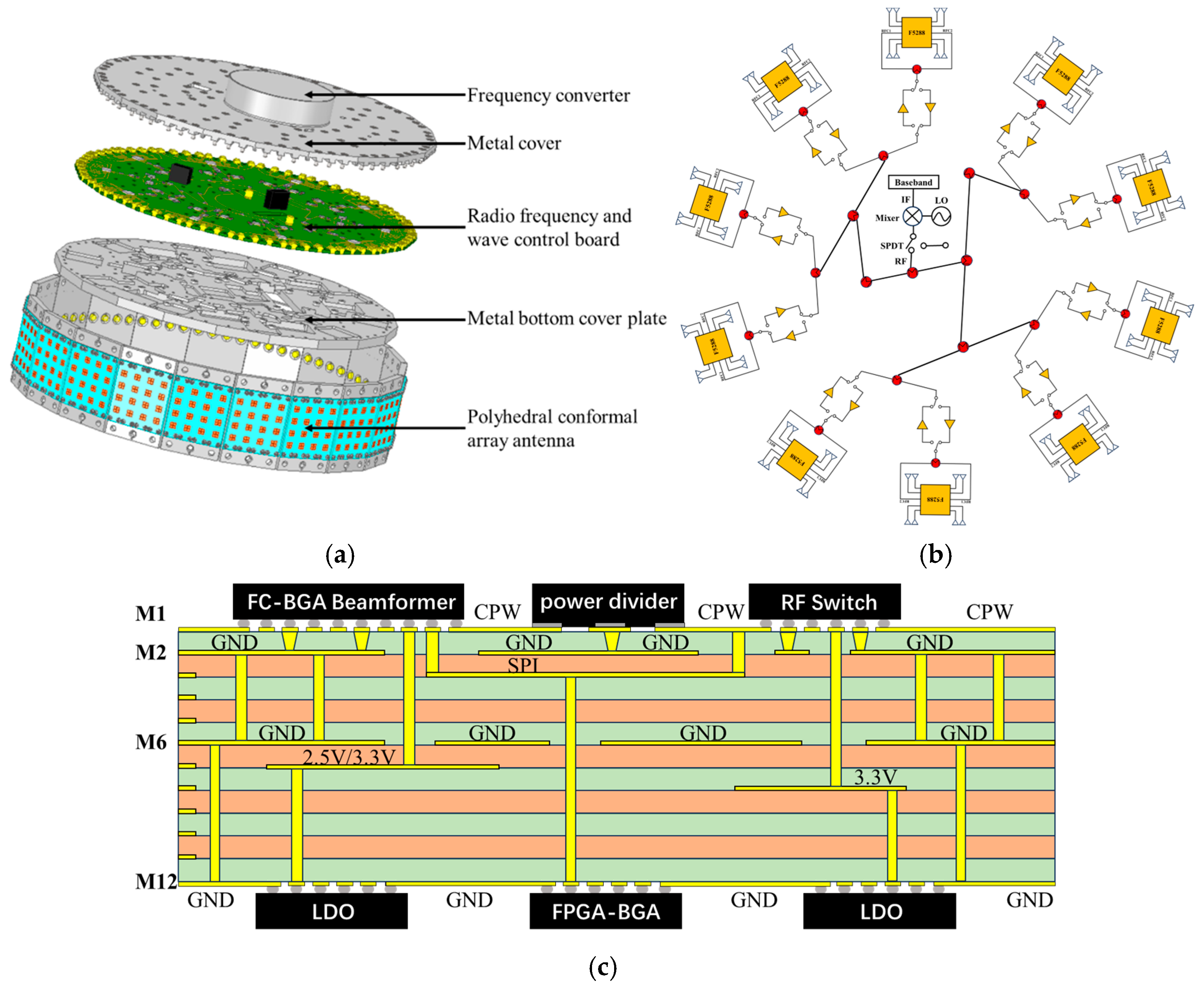
Figure 1. (a) Explosion diagram of a cylindrical conformal transceiver active phased array in Ka-Band. (b) Ka-band cylindrical conformal transceiver active phased-array architecture based on 8-channel TRX chips. (c) Twelve-layer PCB stackup.
Applsci 15 08982 g001
Figure 2. (a) Three-dimensional unit cell model of the metasurface-coupled stacked patch microstrip antenna and the radiation pattern of the antenna element. (b) Simulated impedance bandwidth and gain bandwidth of antenna element.
Applsci 15 08982 g002
Figure 3. (a) Side view of the 3 × 16 antenna subarrays. (b) Simulated impedance and gain bandwidth of the 3 × 16 antenna arrays. (c) Simulated normalized radiation patterns of the array at 28.5 GHz.
Applsci 15 08982 g003
Figure 4. Transceiver channel schematic.
Applsci 15 08982 g004
Figure 5. (a) F5288 output phase compensation line design. (b) Simulation of insertion loss and return loss for phase compensation lines. (c) Simulation of isolation and phase characteristics for phase compensation lines.
Applsci 15 08982 g005aApplsci 15 08982 g005b
Figure 6. (a) Three-dimensional circuit model of polarization synthesis for the 5288 beamforming chip. (b) Surface-mount technology (SMT) design of the Al2O3 ceramic power divider. (c) Simulation results of the 5288 polarization synthesis circuit integrated with the ceramic power divider.
Applsci 15 08982 g006
Figure 7. (a) Power divider network schematic. (b) Power divider network port design. (c) Simula-tion of insertion loss, return loss, port isolation, and phase consistency for the power divider net-work. (d) Simulation Results of Port Isolation and Phase Consistency Across Branches.
Applsci 15 08982 g007
Figure 8. (a) Top-view layout and (b) bottom-view layout of the proposed RF beamforming module.
Applsci 15 08982 g008
Figure 9. The 320-element array RF link based on an 8-channel BNF chip, ADRF5020, and QPA2628.
Applsci 15 08982 g009
Figure 10. (a) Single-channel receive gain performance. (b) Single-channel receive NF performance.
Applsci 15 08982 g010
Figure 11. (a) Single-channel transmit gain performance. (b) Single-channel transmit OP1dB (output 1 dB compression point).
Applsci 15 08982 g011
Figure 12. RF link configuration for G/T evaluation.
Applsci 15 08982 g012
Figure 13. RF link configuration for EIRP evaluation.
Applsci 15 08982 g013
Figure 14. (a) Top view of CCTAPA. (b) Bottom view of CCTAPA. (c) Calibration and measurement setup in a far-field antenna chamber.
Applsci 15 08982 g014
Figure 15. (a) Post-calibration residual amplitude and (b) phase errors at 28.5 GHz.
Applsci 15 08982 g015
Figure 16. (a) Definition and distribution of beamforming chips. (b) Transmit frequency response across different array panels. (c) Receive frequency response across different array panels.
Applsci 15 08982 g016
Figure 17. Simulated versus measured normalized radiation patterns of the array in azimuth plane at (a) 26 GHz, (b) 28.5 GHz, and (c) 31 GHz, with scanning at 0°, ±4.5°, and ±9°.
Applsci 15 08982 g017
Figure 18. Simulated versus measured normalized radiation patterns of the array in elevation plane at (a) 26 GHz, (b) 28.5 GHz, and (c) 31 GHz.
Applsci 15 08982 g018
Figure 19. Gain fluctuation of 10 uniformly distributed beams on axis during 360° scanning at 28.5 GHz.
Applsci 15 08982 g019
Figure 20. (a) G/T measurement of Beam 1 at different frequencies. (b) G/T measurement of 10 beams on axis over 360° at 28.5 GHz.
Applsci 15 08982 g020
Figure 21. (a) EIRP measurement of Beam 1 at different frequencies. (b) EIRP measurement of 10 beams on axis over 360° at 28.5 GHz.
Applsci 15 08982 g021
Table 1. TRX beamforming chip, switch, and LNA summary.
ParameterUnitF5288ADRF5020QPA2628
FrequencyGHz26~310.01~3122~31.5
No. of Channels-811
Work Model TRX--
Package-FCCSPLGAQFN
Insertion LossdB-2@30 GHz-
TX Typical GaindB30.5--
TX Typical OP1dBdBm19.5--
Phase Shifter (PS)bit6--
PS Phase Stepdegree5.625--
TX Typical PS Phase Errordegree rms0.9--
TX VGAbit6--
VGA StepdB0.5--
TX VGA Gain Control RangedB30.5--
TX VGA Gain ErrordB rms0.15--
TX Power/ChannelmW675--
TX Supply VoltageV2.5 V--
RX Typical GaindB17.6-23
Typical Noise FiguredB4.6-1.6
RX Typical IP1dBdBm−28.5-−4
RX Typical PS Phase Errordegree rms1.4--
RX VGAbit5--
VGA StepdB0.5--
RX VGA Gain Control RangedB15.5--
RX VGA Gain ErrordB rms0.1--
RX Power/ChannelmW210-315
RX Supply VoltageV2.53.53.5
Table 2. Correspondence between beamforming chips and beam directions.
Beamforming Chip IdentificationBeam Identification
BF1 and half of BF2Beam 1
BF2 and half of BF3Beam 2
BF3 and half of BF4Beam 3
BF4 and half of BF5Beam 4
BF5 and half of BF6Beam 5
BF6 and half of BF7Beam 6
BF7 and half of BF8Beam 7
BF8 and half of BF9Beam 8
BF9 and half of BF10Beam 9
BF10 and half of BF1Beam 10
Table 3. Comparison with state-of-the-art phased-array antennas.
ReferenceThis work[29][28][23][31][34]
Frequency (GHz)26~316~1210.7~12.758.21252.4~32.55~3.12
Element typePatch antennaPatch antennaPatch antennaWaveguide antennaPatch antennaPatch antenna
PolarizationLinearLinearDual polarizationDual-circularLinearLinear
Modes of operationTRX-RXTX--
Array scale320484 × 8641 × 121 × 8
Array shapeCylindrically ConformalCylindrically ConformalCylindrically ConformalSpherical
Conformal
Wing
Conformal
UAV
Conformal
Active integrationYESNoYesYesNoNo
Array unit numbers/BF chips32-0.54--
Beam steering1D2D2D2D1D1D
Scan range (°)360±60±60360±60±70
Scan gain fluctuation (dB)0.833-21.9
Power per element (W)0.027-1.0689--
Total power (W)8.73-34.17636--
Element size 0.67 λ × 0.67 λ0.48 λ × 0.48 λ0.47 λ × 0.59 λ-0.5 λ × 0.54 λ0.52 λ × 0.21 λ
Disclaimer/Publisher’s Note: The statements, opinions and data contained in all publications are solely those of the individual author(s) and contributor(s) and not of MDPI and/or the editor(s). MDPI and/or the editor(s) disclaim responsibility for any injury to people or property resulting from any ideas, methods, instructions or products referred to in the content.