Article

The Effect of Cs-Controlled Triple-Cation Perovskite on Improving the Sensing Performance of Deep-Ultraviolet Photodetectors

1
Department of Electrical Engineering, Gachon University, Seongnam 13120, Republic of Korea
2
Research and Development, One Tech. Incorporation, Seongnam 13120, Republic of Korea
*
Authors to whom correspondence should be addressed.
Appl. Sci. 2025, 15(14), 7982; https://doi.org/10.3390/app15147982
Submission received: 13 June 2025 / Revised: 14 July 2025 / Accepted: 15 July 2025 / Published: 17 July 2025
(This article belongs to the Section Energy Science and Technology)

Abstract

In this study, a UVC photodetector (PD) was fabricated by incorporating CsI into a conventional double-cation perovskite (FAMAPbI3) to enhance its stability. The device utilized a methylammonium iodide post-treatment solution to fabricate CsFAMAPbI3 perovskite thin films, which functioned as the primary light-absorbing layer in an NIP structure composed of n-type SnO2 and p-type spiro-OMeTAD. Perovskite films were fabricated and analyzed as a function of the Cs concentration to optimize the Cs content. The results demonstrated that Cs doping improved the crystallinity and phase stability of the films, leading to their enhanced electron mobility and photodetection performance. The UVC PD with an optimum Cs concentration exhibited a responsivity of 58.2 mA/W and a detectivity of 3.52 × 10¹⁴ Jones, representing an approximately 7% improvement over conventional structures.

1. Introduction

Photodetectors (PDs), also known as photosensors, are devices designed to detect specific types of light (such as ultraviolet (UV), visible, and infrared) or other forms of electromagnetic radiation. PDs function as optical-to-electrical (O/E) converters that convert light from specific spectral regions into electrical output signals, such as voltages or currents, similar to photovoltaic devices [1,2,3,4]. They are widely used in various applications such as video imaging, biomedical image sensing [5,6,7], optical communication [8], military-related systems [9], aerospace technologies [10], and industrial processes [11].
To date, PDs have primarily been fabricated using inorganic semiconductor-based materials (e.g., silicon, III-V semiconductors, oxide or metal complexes, and alloys). However, inorganic semiconductor systems are fabricated under vacuum conditions, which involve high costs and complex manufacturing processes. In contrast, organic-based device fabrication processes offer advantages, such as low temperature and simplicity, compared with commercial semiconductor fabrication processes.
Moreover, ABX3 perovskites have emerged as potential candidate materials for PDs because of their good optical (tunable wide bandgap and high light absorption) and electrical (high carrier mobility and long diffusion length) properties [12].
Recent studies have explored the potential of perovskite materials for UV and deep-ultraviolet (UVC) PD applications. One study demonstrated a self-powered UVC PD based on a mixed-halide perovskite ((FAPbI3)0.97(MAPbBr3)0.03), which exhibited high responsivity (52.68 mA/W) and high response speed under 254 nm UV light without requiring an external power supply. The device also maintained stable performance after being stored in air for three weeks.
In addition, the tunability of the perovskite bandgap has been leveraged to develop sensors with enhanced sensitivity to short-wavelength UV light, enabling improved detection precision and environmental stability. One study employed a fluoropolymer-coated CH3NH3PbI3-xClx perovskite structure that achieved high responsivity (7.85 A/W), sub-microsecond response time, and long-term durability, maintaining stable operation even after 100 days of air exposure. A clear photoresponse at 254 nm was confirmed, and further evaluations across the UVA, UVB, and visible wavelength regions are planned for future studies.
In particular, double-cation perovskites (FAMAPbI3), which incorporate formamidinium (FA) and methylammonium (MA) cations, have been extensively studied for UVC PD applications owing to their excellent optoelectronic properties.
Despite their advantages, double-cation perovskites suffer from inherent stability issues, particularly under thermal stress and in humid environments. Methylammonium-based perovskites are prone to decomposition because of the volatility of MA cations, which leads to performance degradation over time. Additionally, FA-based perovskites, while offering better stability than their MA-based counterparts, still face challenges in maintaining structural integrity under prolonged exposure to heat and moisture [13,14,15,16].
In previous studies, various approaches have been attempted to address the stability issues of double-cation perovskites (FAMAPbI3). However, fully resolving their thermal and moisture stability limitations remains challenging. In this study, we introduced a triple-cation (CsFAMAPbI3) structure [17] and applied a two-step post-treatment process (methylammonium iodide (MAI)–isopropyl alcohol (IPA) treatment) to enhance the crystallinity of the structure and minimize its surface defects, thereby significantly improving stability compared with conventional methods [18].
This study aims to demonstrate that a triple-cation perovskite-based UVC PD offers superior optoelectronic performance, enhanced stability, and improved durability compared with conventional double-cation structures.

2. Materials and Methods

2.1. Chemical Reagents

Lead(II) iodide (PbI2, 99.999%), formamidinium iodide (FAI), MAI, sodium dodecylbenzenesulfonate (SDBS), 1-butanol (99%), ethyl alcohol (≥99.5%), acetonitrile (99.93%), N,N-dimethylformamide (DMF, 99.8%), dimethyl sulfoxide (DMSO, ≥99.9%), IPA (75 wt%), 2,2,7,7-tetrakis[N,N-di(4-methoxyphenyl)amino]-9,9-spirobifluorene (Spiro-OMeTAD, 99%), lithium bis(trifluoromethanesulfonyl)imide (Li-TSFI; ≥99.0%), chlorobenzene (99.8%), toluene (99.9%), diethyl ether (≥99.7%), and 4-tert-butylpyridine (98%) were purchased from Sigma-Aldrich (St. Louis, MO, USA). Methylammonium hydrochloride (MACl) was purchased from GreatCell Solar (Queanbeyan, Australia). SnO2 colloidal solution (15 wt% in water) was obtained from Alfa Aesar (Seoul, Republic of Korea). Indium tin oxide (ITO) coated on quartz glass substrates (160 nm thickness) was acquired from TMA (Seoul, Republic of Korea). All the reagents were used as received without further purification.

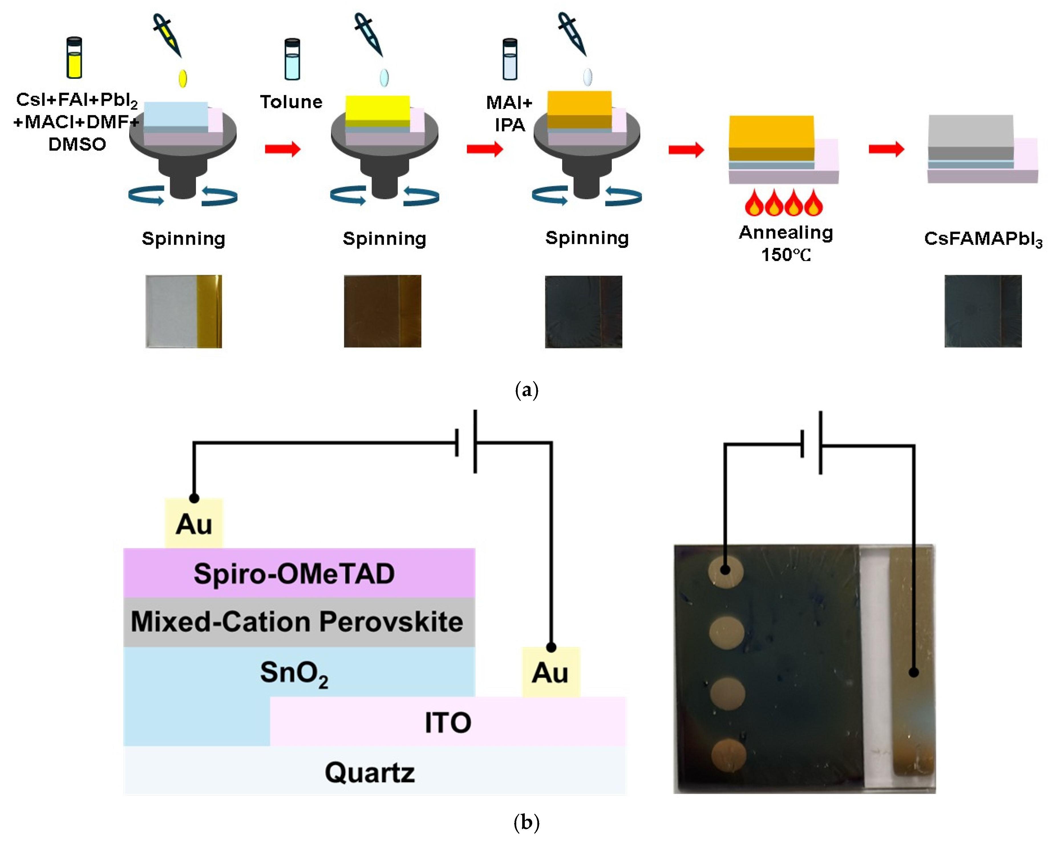
2.2. Sample Fabrication Process

2.2.1. Substrate Preparation

ITO-coated quartz substrates (8 Ω m−2) were sequentially cleaned using an ultrasonic bath with neutral detergent, IPA, ethanol, and deionized water for 20 min each. The cleaned substrates were then dried at 80 °C for at least 30 min in a drying oven. After drying, polymer tape was attached to the substrate, followed by UV treatment using a UV lamp for 15 min to ensure surface cleanliness.

2.2.2. SnO2 Deposition

A SnO2-SDBS mixed solution was prepared by diluting 1.2 mL of SnO2 colloidal solution (15 wt%) with 5.2 mL of deionized water, followed by dissolving 1 mg of SDBS. The resulting solution was spin-coated onto cleaned ITO substrates at 2000 rpm for 25 s. The coated substrates were subsequently annealed at 150 °C for 30 min to form the electron transport layer. Before the perovskite deposition, the substrates were subjected to a second UV–ozone treatment for 15 min.

2.2.3. Perovskite Film Deposition

Unlike in conventional solution-processed perovskites, a two-step post-treatment method was used to improve the quality and stability of the perovskite films. First, a precursor solution containing Cs, FA, and Pb was deposited to form a (Cs0.05FA0.95)PbI3 perovskite layer.
The CsFAPbI3 precursor solution was prepared by dissolving PbI2 (1.4 M), CsI (0.07 M), and FAI (1.33 M) in a DMSO:DMF (10:1, v/v) solvent system, corresponding to a molar ratio of Cs:FA = 0.05:0.95. This ensured that the total concentration of the A-site cation was equal to that of the B-site cation (Pb2+), maintaining the stoichiometry of Cs0.05FA0.95PbI3. MACl (0.1 M) was added to the precursor solution to promote grain growth and improve crystallinity, and the mixture was stirred for 30 min. The solution was filtered through a 0.45 μm syringe filter immediately before spin-coating. The precursor solution was deposited onto the substrates at 4000 rpm for 25 s. To induce rapid crystallization, 100 μL of toluene was dropped onto the spinning substrate 5 s after the start of spinning as an anti-solvent. This step promoted uniform nucleation and facilitated the formation of dense and pinhole-free perovskite films. After spin-coating, a post-treatment was performed using a solution of MAI (20 mg) in IPA under the same spin-coating conditions. The films were then annealed at 150 °C for 15 min to ensure complete crystallization.
The manufacturing process for the triple mixed-cation perovskite (CsFAMAPbI3) and the schematic illustrating the device architecture for the perovskite-based PD are shown in Figure 1.
After the deposition of the initial perovskite layer, a post-treatment was applied to enhance crystallinity and reduce surface defects. A solution of MAI (20 mg) in IPA (1 mL) was spin-coated onto the perovskite layer under the same spin conditions (4000 rpm, 25 s). This post-treatment is known to passivate surface traps and improve film uniformity. The treated films were subsequently annealed at 150 °C for 15 min to promote complete crystallization.
Previous studies have shown that such an MAI–IPA treatment can induce surface recrystallization and passivate shallow trap states, thereby enhancing the optoelectronic quality of perovskite films [19]. Although trap density and carrier lifetime were not directly measured in this work, improvements in grain size, optical absorption, and charge transport characteristics provided indirect evidence of the treatment’s effectiveness.

2.2.4. Hole Transport Layer and Electrode Deposition

After annealing, the substrates were allowed to cool to room temperature (18–25 °C) for 30 min. A spiro-OMeTAD solution was then deposited onto the perovskite film by spin-coating at 2000 rpm for 25 s. The spiro-OMeTAD solution was prepared by dissolving 72.3 mg of spiro-OMeTAD, 28.8 μL of 4-tert-butylpyridine (tBP), and 17.5 μL of a Li-TFSI solution (520 mg Li-TFSI in 1 mL of acetonitrile) in 1 mL of chlorobenzene.
Finally, an 80 nm thick gold (Au) electrode was thermally evaporated on top of the hole transport layer under high-vacuum conditions (2 × 10⁻⁶ Torr), completing the fabrication of the UVC PD device.

2.3. Sample Measurements

2.3.1. Structural and Morphological Analysis

The crystal structures of the perovskite films were analyzed using high-resolution X-ray diffraction (XRD; SmartLab, Rigaku, Tokyo, Japan) with Cu-Kα radiation (λ = 1.542 Å). The surface morphologies and grain structures were examined using field-emission scanning electron microscopy (FE-SEM; Hitachi S-4700, Tokyo, Japan).

2.3.2. Optical Characterization+

The optical absorption properties of the perovskite films were measured using a UV–Visible (UV-Vis) spectrophotometer (Agilent 8453, Santa Clara, CA, USA). Tauc plot analysis was used to estimate the optical bandgap of the films, where (αhν)2 was plotted against the photon energy (hν) based on the absorption spectra.

2.3.3. Electrical and PD Performance

The electrical and optoelectronic performances of the perovskite-based UVC PDs were measured using a source-measure unit (Keithley 2400, Cleveland, OH, USA). All the measurements were conducted under ambient air conditions at room temperature (18–25 °C) inside a dark chamber to minimize the interference from external light.
A portable UVC lamp (UVGL-58, Analytik Jena, Jena, Germany) with a wavelength of 254 nm was used as the excitation source. The lamp was positioned approximately 10 cm away from the device surface. According to the manufacturer’s specifications, the light intensity at this distance was estimated to be approximately 1.2–1.5 mW/cm2. The active area of each device was approximately 2.0 cm × 1.5 cm.
The devices were mounted onto a custom-designed test jig to ensure stable and reproducible electrical contacts during the measurement. The current–voltage (I–V) characteristics were obtained by sweeping the bias voltage from +1 V to −1 V in 0.1 V increments.
For photocurrent response measurements, the UVC light was periodically modulated at 10 s on/off intervals using an Arduino-controlled servomotor system. Each measurement was repeated five times to ensure reproducibility.

3. Results and Discussion

3.1. Characterization of Triple-Cation Perovskite Thin Films

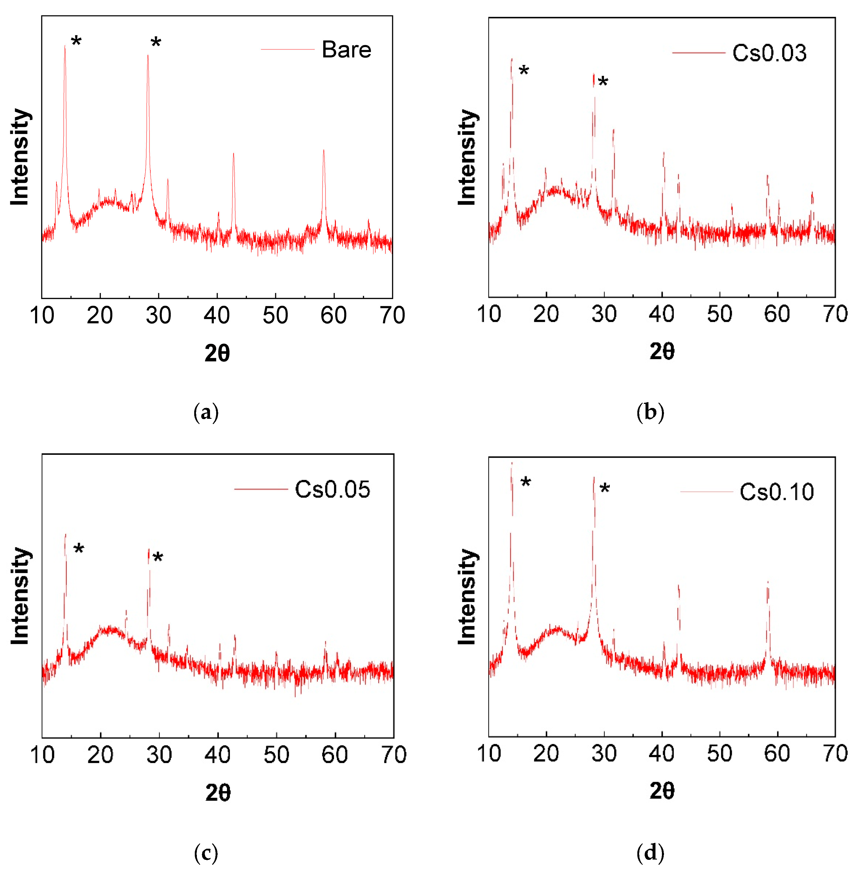
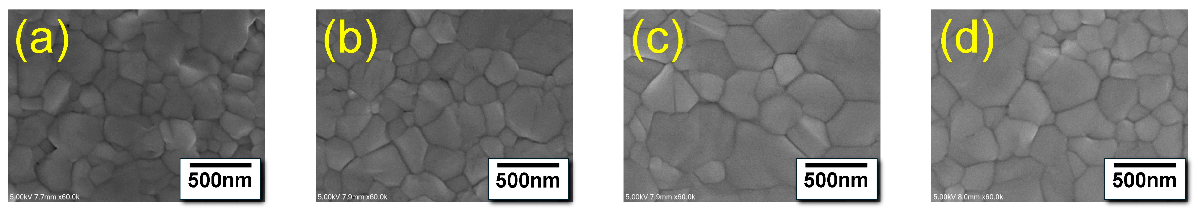
3.1.1. Structural Analysis of Triple-Cation Perovskite Thin Films

The structural characteristics of the triple mixed-cation (Cs, FA, MA)-based perovskites were analyzed using X-ray diffraction (XRD). The XRD patterns in Figure 2 illustrate the changes in the crystal structure of the perovskite films as a function of the Cs content.
The main diffraction peaks in the XRD patterns appeared at approximately 14.1° and 28.4°, corresponding to the (110) and (220) planes of the perovskite structure, respectively. These peaks are similar to those of the double-cation (FAMAPbI3) perovskite, indicating that the perovskite crystal structure is well maintained in the triple mixed-cation system [20]. The incorporation of Cs, with a smaller ionic radius (1.81 Å) than that of FA+ (2.53 Å), induces lattice contraction and forms a more compact crystal structure. This structural change can reduce the defect density and improve stability [21]. The main diffraction peaks are marked with asterisks in Figure 2 (at approximately 14.1° and 28.4°).
Additionally, the main diffraction peaks of the α-phase perovskite were maintained even after the incorporation of Cs. Notably, these α-phase peaks remained visible at Cs concentrations of 0.05 and 0.10, suggesting that the triple mixed-cation structure may offer superior thermal and environmental stability than the double-cation structure. While the peak intensity of the Cs0.1 sample was slightly stronger than that of Cs0.05 (as shown in Figure 2c,d), the XRD results confirmed that the addition of Cs did not interfere with the formation of the perovskite crystal phase. Among the tested Cs compositions, Cs = 0.05 was found to be an optimal concentration that supported phase stability without introducing secondary phases.
Similar trends have been reported in previous studies on triple-cation perovskite solar cells. For example, Ašmontas et al. reported that Cs incorporation contributes to lattice contraction and improved crystallinity while preserving the structural stability [22]. A follow-up study by the same group demonstrated that an optimal Cs content can enhance the photoelectric performance of both planar and mesoporous device structures [23]. These findings are consistent with our structural analysis, which suggests that moderate Cs incorporation leads to uniform and stable perovskite films.
Considering the Goldschmidt tolerance factor and octahedral factor values, the Cs-incorporated perovskite structure remained within a stable range, indicating that the Cs addition did not adversely affect the structural stability of the double-cation perovskite. The XRD patterns revealed that no secondary phases were induced by Cs incorporation, confirming the successful formation of a homogeneous and stable triple-cation perovskite.
The Goldschmidt tolerance factor (t) and octahedral factor (μ) were calculated to evaluate the crystal structures of the Cs, FA, and MA triple-cation (CsFAMAPbI3) perovskites [20]. Table 1 shows the variations in the tolerance and octahedral factors for the bare (FAMAPbI3) and Cs-doped conditions (Cs0.03, 0.05, and 0.10). The Goldschmidt tolerance factor is defined as
t = r A + r X 2 ( r B + r X )
The effective ionic radius of the A-site cation (rA), a mixture of Cs+, FA+, and MA+, was determined based on XRD analysis. Similarly, the B-site cation (rB) and halide anion (rx) radii were derived from the XRD data. Generally, perovskites are considered structurally stable in the cubic or slightly distorted cubic phase when 0.9 ≤ t ≤ 1.0 [24].
The calculated tolerance factors for the bare and Cs-doped samples (Table 1) indicate that all the samples remained within the stable perovskite structure region. Even with an increase in the Cs content, the tolerance factor remained within a stable range. As confirmed by XRD analysis, despite Cs+ having a smaller ionic radius than FA+ and MA+, the incorporation of Cs does not compromise the stability of the structure. The crystal structure remained stable even with an increase in the Cs content. The octahedral factor is defined as follows:
μ = r B r X
The values of rB and rX for the Pb–I system were derived from XRD analysis, and the octahedral factor (μ) was calculated, showing similar values of 0.54 across all the Cs-doping conditions (Table 1). This suggests that A-site cation substitution does not significantly affect the structural stability of the PbI6 octahedra [24].
These results demonstrate that adjusting the tolerance factor through Cs doping can optimize the perovskite crystal structure while maintaining the octahedral factor within a stable range. Therefore, the structural stability of the material was preserved, confirming the feasibility of the proposed Cs-doping strategy for fabricating perovskite thin films with structural properties suitable for UVC PD applications.
Scanning electron microscopy (SEM) analysis was used to further investigate the structural characteristics of the mixed-cation perovskite films, as shown in Figure 3. The SEM images revealed the morphological evolution of the perovskite films with increasing Cs content.
The average grain size increased with an increase in the Cs content, reaching a maximum value at Cs = 0.05. Compared with the pristine FAMAPbI3 film, which exhibited a smaller grain size, the Cs-incorporated films showed a noticeable increase in the grain size, particularly at Cs = 0.05, as can be clearly observed from the SEM images shown in Figure 3.
However, when the Cs content exceeded 0.05 (Cs = 0.07 and 0.10), the grain size decreased. This reduction in the grain size at higher Cs concentrations can be attributed to excessive lattice contraction and an increase in the number of nucleation sites. The smaller ionic radius of Cs+ (1.81 Å) compared with that of FA+ (2.53 Å) induces lattice shrinkage, leading to internal strain that hinders further crystal growth. Additionally, excessive Cs incorporation can increase the number of nucleation sites, limiting continued grain growth [25,26].
The SEM images indicated that, while Cs incorporation promoted grain growth up to a certain level, an excessive Cs content resulted in reduced grain size. Thus, careful optimization of the Cs concentration was essential to achieve the desired balance between structural stability and grain morphology for optimal device performance.
In particular, the Cs0.05 composition represents an optimal balance between lattice stabilization and lattice distortion. Excessive Cs incorporation increases lattice strain, which can introduce defects and non-uniformities at the grain boundaries, ultimately leading to performance degradation. This interpretation is supported by previous studies showing that Cs incorporation positively affects band alignment, charge transport, and defect passivation [27].

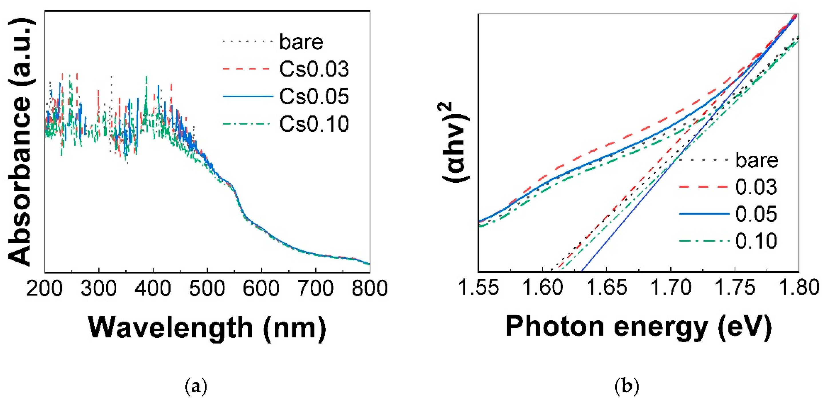
3.1.2. Optical Properties of Mixed-Cation Perovskite Thin Films

To investigate the optical properties of the fabricated perovskite thin films, UV-Vis absorption spectroscopy and Tauc plot analyses were performed, and the results are shown in Figure 4.
Figure 4a shows the absorption spectra of pure and Cs-incorporated (Cs = 0.03, 0.05, and 0.10) FAMAPbI3 thin films. All the films exhibited strong absorption characteristics in the UV-Vis region. With the incorporation of Cs, the absorption of the films increased, with the most significant increase observed at Cs = 0.05. This suggests that Cs incorporation enhanced the crystallization of the films and reduced their defect density, leading to improved light-absorption properties.
Figure 4b shows the results of the Tauc plot analysis, where (αhν)2 is plotted against the photon energy (hν). With an increase in the Cs content, the absorption edge shifted, indicating a change in the optical bandgap of the films.
The pure FAMAPbI3 thin film (Figure 4b, dotted line) showed a basic bandgap, which increased with the introduction of Cs. The highest bandgap was observed at Cs = 0.05 (solid line), while at Cs = 0.10 (dash-dot line), the bandgap decreased again. These results indicate that the introduction of Cs affected the crystal structure and defect states of the thin films, resulting in changes in their electronic structure.
The increase in the bandgap can be interpreted as the optimal amount of Cs adjusting the lattice structure, reducing defects, and enhancing crystallinity. However, when the Cs content was increased to 0.10, the bandgap decreased again, likely because of the lattice contraction and increased structural disorder caused by excess Cs [26].
Although the Cs content in our samples was relatively low (up to 0.10), we acknowledge that the non-monotonic trend in the bandgap values could also arise from local structural inhomogeneities or early-stage phase segregation, as reported in previous studies [28]. Further investigations, such as PL mapping or grazing-incidence wide-angle X-ray scattering (GIWAXS), would be required to confirm the phase purity in future works.

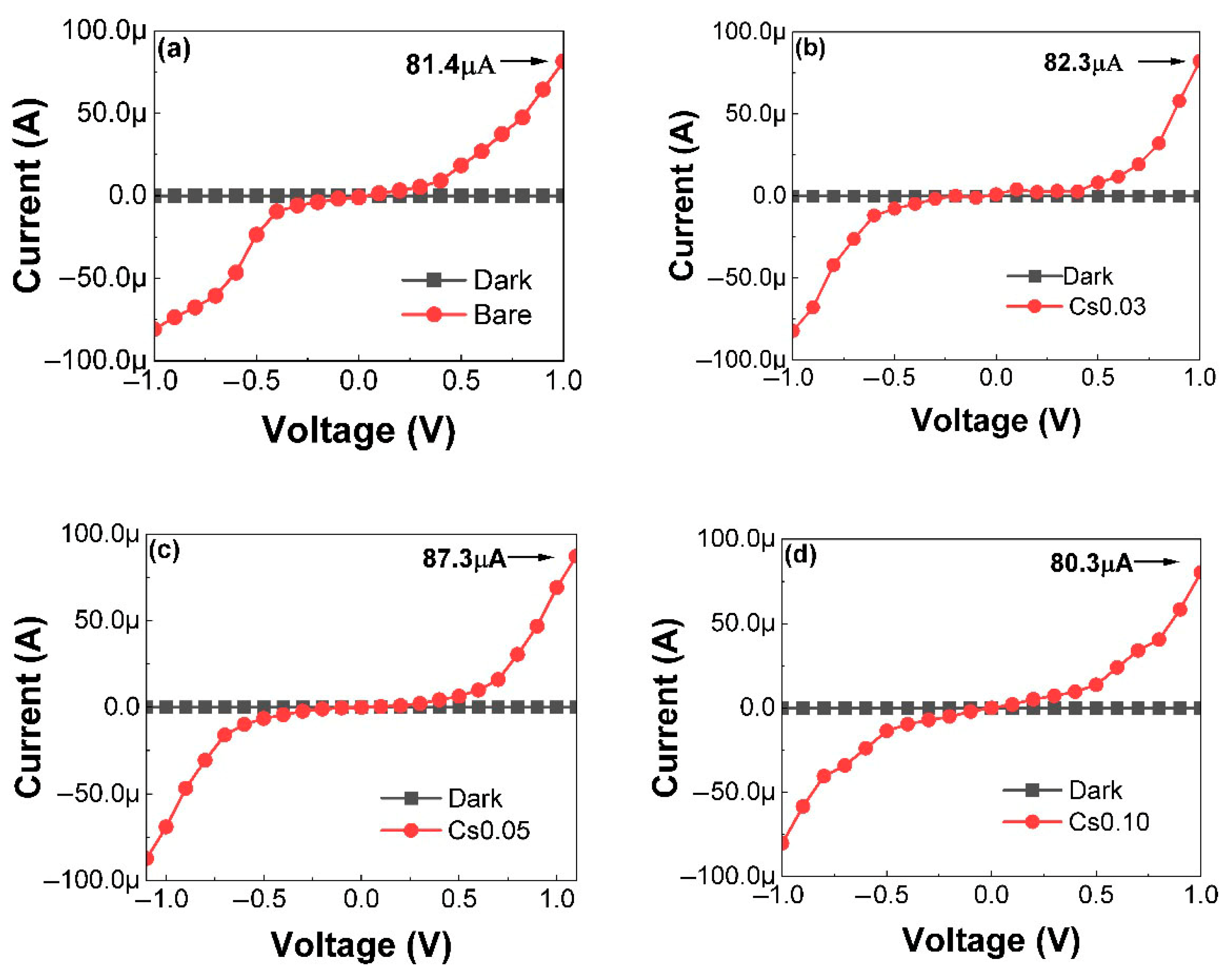
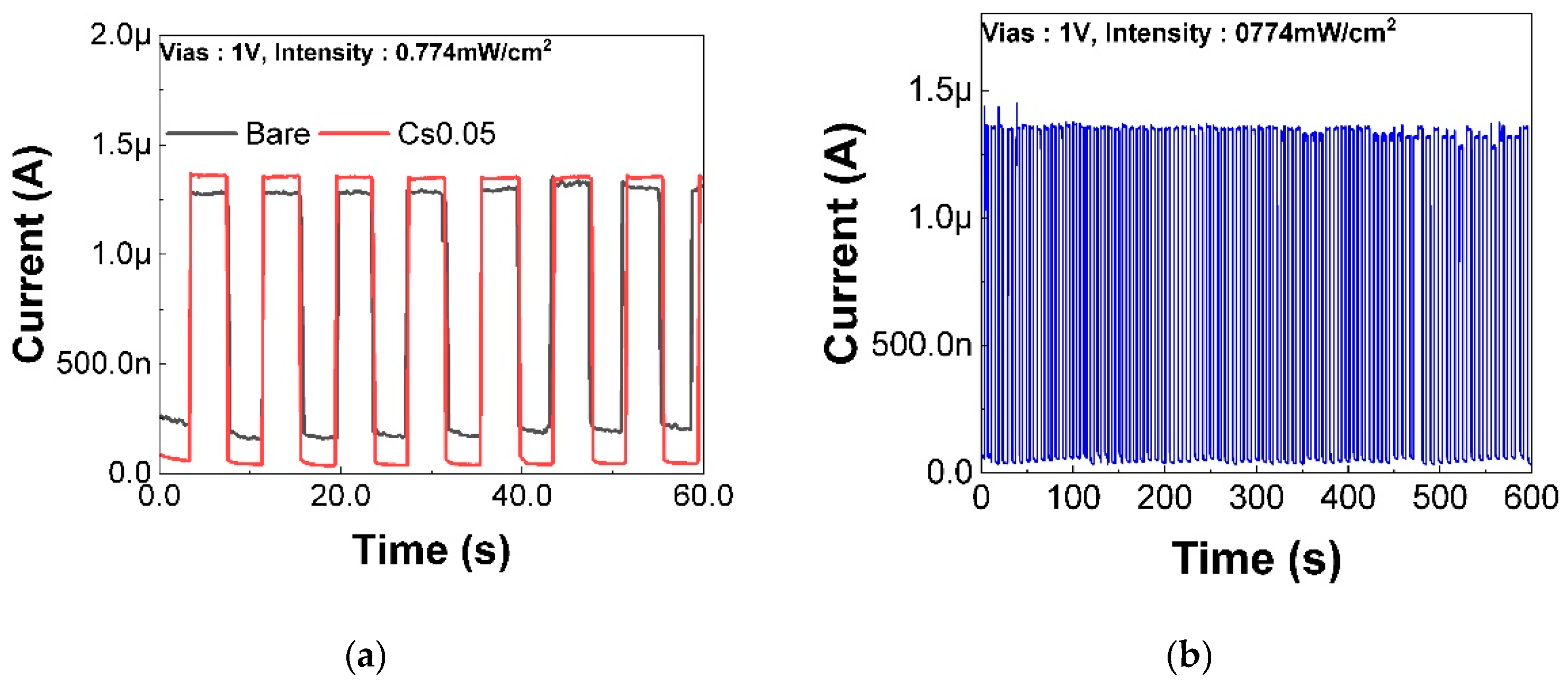
3.1.3. Performance Evaluation of Sensors with Triple-Cation Perovskite Structure

To evaluate the performance of the light sensor incorporating a triple mixed-cation (CsFAMAPbI3) perovskite, the I-V characteristics were measured. As shown in Figure 5, the bare (FAMAPbI3) sample showed a current of 81.4 μA. At a Cs concentration of 0.03, the current of the film increased to 82.3 μA, which further increased to 87.3 μA at Cs = 0.05. At Cs = 0.10, the current decreased to 80.3 μA. This indicates that Cs incorporation significantly affected the electrical properties of the FAMAPbI3 film and that the optimum Cs concentration enhanced the performance of the sensor.
The changes in the electrical characteristics with increasing Cs concentration may be attributed to the influence of the grain size. As the Cs content increased, the grain size increased, resulting in a reduced number of grain boundaries and enhanced charge mobility. In particular, up to Cs = 0.05, the increased grain size reduced the charge scattering, leading to an increase in the current. However, at Cs = 0.10, supersaturation hindered crystal growth, which decreased the grain size and increased the number of grain boundaries. This, in turn, promoted charge recombination and caused a decrease in the current.
These findings confirm that precise control of the Cs concentration is a critical factor in optimizing the electrical properties of light sensors. Notably, the Cs0.05 sample exhibited the highest current value, demonstrating the optimal electrical performance within the triple mixed-cation perovskite structure.
To evaluate the optoelectronic performance of the CsFAMAPbI3 perovskite-based PDs, their responsivity (R) and detectivity (D*) were analyzed, as shown in Figure 6. The results indicated that both R and D* increased with increasing Cs incorporation up to Cs = 0.05, reaching maximum values of approximately 58.2 mA/W and 3.52 × 10¹⁴ Jones, respectively. This enhancement can be attributed to the improved charge transport and reduced recombination owing to the optimized grain size and crystallinity. However, at Cs = 0.10, a decline in device performance was observed, likely because the excessive Cs content led to crystallographic defects and an increased number of grain boundaries.

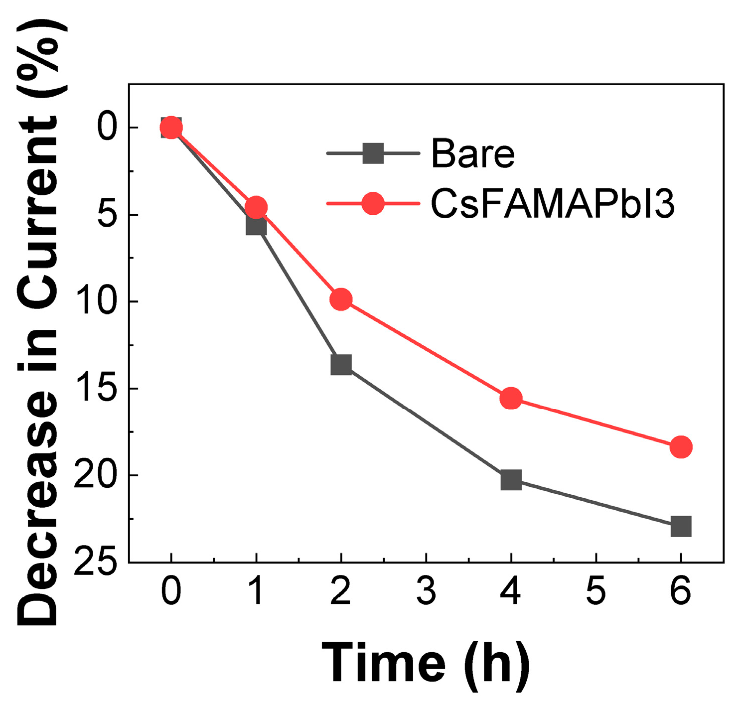
3.2. Stability of Sensors with Triple-Structure Perovskite

Figure 7 shows the UVC on/off response characteristics and the long-term operational stability of the fabricated sensor. As shown in Figure 7a, both the bare sensor and the sensor containing Cs0.05 exhibited a consistent current response when the UVC was turned on and off at periodic time intervals. Notably, the Cs0.05 sensor maintained a higher current response than the bare sensor, with the signal shape remaining distinct and stable.
Figure 7b shows the current response when the sensor was operated for an extended period. The signal maintained a consistent pattern with no significant flicker or drift, which indicates that the fabricated sensor could maintain a relatively stable operation even under prolonged UVC exposure.
Thus, the perovskite-based UVC PD developed in this study demonstrated reliable performance during both repetitive on/off and long-term operations.
To evaluate the long-term reliability of the sensor, its current degradation behavior over time was analyzed. Figure 8 shows the current degradation rates (%) of the double-cation (FAMAPbI3) and optimized triple-cation (Cs0.05FA0.9MA0.1PbI3) devices. Each sample was measured immediately after fabrication and again at 1, 2, 4, and 6 h. All the I–V measurements were performed under a 1 V bias and 254 nm UV illumination, while the samples were stored under room-temperature conditions inside a glove box between measurements. The Cs+ concentration in the triple-cation device was fixed at x = 0.05, which was identified as the optimal composition in this study.
The results showed that both the devices experienced a decrease in current over time. After 6 h, the FAMAPbI3 device exhibited a current degradation of approximately 23.0%, whereas the CsFAMAPbI3 device exhibited a relatively low degradation of approximately 18.4%. This indicates that the incorporation of Cs into the triple-cation perovskite contributed to improved environmental stability.
These results indicate that the optimized triple-cation device maintained a more stable photocurrent over time than its double-cation counterpart. Although the difference was modest, the incorporation of Cs contributed to improved operational stability under sustained UV exposure, enhancing the long-term photoresponse characteristics of the sensor.
The performances of the perovskite PDs were compared with those of other materials in terms of light responsiveness, detection wavelength, on/off ratio, and detectivity (Table 2).

4. Conclusions

In this study, we proposed a novel approach to enhance the photodetection and stability of triple-cation perovskites (CsXFA0.9MA0.1PbI3) through compositional engineering and MAI post-treatment, without the need for the introduction of new materials we fabricated a triple-cation (CsFAMAPbI3) perovskite-based UVC PD and compared its electrical properties and stability with those of a conventional double-cation (FAMAPbI3) perovskite-based sensor. We systematically evaluated the photoelectric performance and durability of the PD by optimizing the Cs concentration. The XRD results confirmed that the double-cation perovskite maintained its crystal structure even after the incorporation of Cs. The characteristic diffraction peaks of the α-phase perovskite were preserved. Notably, at Cs = 0.05, the diffraction peaks exhibited enhanced intensity and a sharper definition, indicating an increase in crystallinity and the formation of a denser lattice. This suggests that Cs incorporation reduces the defect density and enhances the overall structural stability of perovskite thin films.
The sensor with the optimum Cs concentration of 0.05 showed the best performance. The photocurrent increased by 7.25%, while the responsivity (R) and detectivity (D*) reached the maximum values of 58.2 mA/W and 3.52 × 10¹⁴ Jones, respectively. Furthermore, the CsFAMAPbI3-based sensor exhibited superior long-term stability, showing a 4.6% improvement compared with its double-cation counterpart, thereby demonstrating enhanced durability. The incorporation of Cs contributed to improved structural stability, as confirmed by the analysis of the Goldschmidt tolerance and octahedral factors, which indicated that the Cs-doped structure remained stable.
Our fabricated triple-cation (CsFAMAPbI3) perovskite-based UVC PD outperformed conventional double-cation perovskite structures in terms of photoelectric performance and long-term stability. These findings suggest that the developed sensor holds significant potential for application in high-performance, long-term stable UVC PDs and other optoelectronic devices in which stability and efficiency are critical.
Recent developments in flexible, self-powered UV detectors employ different materials and device architectures, making direct comparison challenging [33]. Therefore, future work may explore the integration of this system into flexible or self-powered devices.

Author Contributions

Investigation, J.S.K.; supervision, H.W.C. and S.K.; validation, H.W.C. and S.K.; writing—original draft, J.S.K.; writing—review and editing, H.W.C. and S.K. All authors have read and agreed to the published version of the manuscript.

Funding

This study was supported by the Gachon University Research Fund 2023 (GCU-202400630001).

Institutional Review Board Statement

Not applicable.

Informed Consent Statement

Not applicable.

Data Availability Statement

The original contributions presented in the study are included in the article, further inquiries can be directed to the corresponding author.

Conflicts of Interest

Author Sangmo Kim was employed by the company One Tech. Incorporation. The remaining authors declare that the research was conducted in the absence of any commercial or financial relationships that could be construed as a potential conflict of interest.

References

  1. Qadir, A.; Shafique, S.; Iqbal, T.; Ali, H.; Xin, L.; Ruibing, S.; Shi, T.; Xu, H.; Wang, Y.; Hu, Z. Recent advancements in polymer-based photodetector: A comprehensive review. Sens. Actuators A Phys. 2024, 370, 115267. [Google Scholar] [CrossRef]
  2. Miao, J.; Zhang, F. Recent progress on highly sensitive perovskite photodetectors. J. Mater. Chem. C 2019, 7, 1741–1791. [Google Scholar] [CrossRef]
  3. Rehman, W.; McMeekin, D.P.; Patel, J.B.; Milot, R.L.; Johnston, M.B.; Snaith, H.J.; Herz, L.M. Photovoltaic mixed-cation lead mixed-halide perovskites: Links between crystallinity, photo-stability and electronic properties. Energy Environ. Sci. 2017, 10, 361–369. [Google Scholar] [CrossRef]
  4. Razeghi, M.; Rogalski, A. Semiconductor ultraviolet detectors. J. Appl. Phys. 1996, 79, 7433–7473. [Google Scholar] [CrossRef]
  5. Jansen-van Vuuren, R.D.; Armin, A.; Pandey, A.K.; Burn, P.L.; Meredith, P. Organic photodiodes: The future of full color detection and image sensing. Adv. Mater. 2016, 28, 4766–4802. [Google Scholar] [CrossRef] [PubMed]
  6. Tian, W.; Zhou, H.; Li, L. Hybrid organic–inorganic perovskite photodetectors. Small 2017, 13, 1702107. [Google Scholar] [CrossRef]
  7. Sang, L.; Liao, M.; Sumiya, M. A comprehensive review of semiconductor ultraviolet photodetectors: From thin film to one-dimensional nanostructures. Sensors 2013, 13, 10482–10518. [Google Scholar] [CrossRef]
  8. Zhao, Z.; Xu, C.; Niu, L.; Zhang, X.; Zhang, F. Recent progress on broadband organic photodetectors and their applications. Laser Photonics Rev. 2020, 14, 2000262. [Google Scholar] [CrossRef]
  9. Žigulić, N.; Glučina, M.; Lorencin, I.; Matika, D. Military decision-making process enhanced by image detection. Information 2023, 15, 11. [Google Scholar] [CrossRef]
  10. Javaid, M.; Haleem, A.; Singh, R.P.; Rab, S.; Suman, R. Significance of sensors for industry 4.0: Roles, capabilities, and applications. Sens. Int. 2021, 2, 100110. [Google Scholar] [CrossRef]
  11. Zhang, X.; Jiang, J.; Feng, B.; Song, H.; Shen, L. Recent Progress in Organic Photodetectors and their Applications. Adv. Sci. 2020, 7, 1902585. [Google Scholar] [CrossRef]
  12. Wang, H.; Sun, Y.; Chen, J.; Wang, F.; Han, R.; Zhang, C.; Kong, J.; Li, L.; Yang, J. A review of perovskite-based photodetectors and their applications. Nanomaterials 2022, 12, 4390. [Google Scholar] [CrossRef] [PubMed]
  13. Lee, J.W.; Seol, D.J.; Cho, A.N.; Park, N.G. High-efficiency perovskite solar cells based on the black polymorph of HC (NH2)2PbI3. Adv. Mater. 2014, 26, 4991–4998. [Google Scholar] [CrossRef] [PubMed]
  14. Stoumpos, C.C.; Malliakas, C.D.; Kanatzidis, M.G. Semiconducting tin and lead iodide perovskites with organic cations: Phase transitions, high mobilities, and near-infrared photoluminescent properties. Inorg. Chem. 2013, 52, 9019–9038. [Google Scholar] [CrossRef] [PubMed]
  15. Jeon, N.J.; Noh, J.H.; Yang, W.S.; Kim, Y.C.; Ryu, S.; Seo, J.; Seok, S.I. Compositional engineering of perovskite materials for high-performance solar cells. Nature 2015, 517, 476–480. [Google Scholar] [CrossRef]
  16. Pellet, N.; Gao, P.; Gregori, G.; Yang, T.Y.; Nazeeruddin, M.K.; Maier, J.; Grätzel, M. Mixed-organic-cation Perovskite photovoltaics for enhanced solar-light harvesting. Angew. Chem. Int. Ed. 2014, 53, 3151–3157. [Google Scholar] [CrossRef] [PubMed]
  17. Saliba, M.; Matsui, T.; Domanski, K.; Seo, J.Y.; Ummadisingu, A.; Zakeeruddin, S.M.; Correa-Baena, J.-P.; Tress, W.R.; Abate, A.; Hagfeldt, A.; et al. Incorporation of rubidium cations into perovskite solar cells improves photovoltaic performance. Science 2016, 354, 206–209. [Google Scholar] [CrossRef]
  18. Chen, H. Two-Step Sequential Deposition of Organometal Halide Perovskite for Photovoltaic Application. Adv. Funct. Mater. 2017, 27, 1605654. [Google Scholar] [CrossRef]
  19. Kang, D.H.; Kim, S.Y.; Lee, J.W.; Park, N.G. Efficient surface passivation of perovskite films by a post-treatment method with a minimal dose. J. Mater. Chem. A 2021, 9, 3441–3450. [Google Scholar] [CrossRef]
  20. Kong, T.; Kim, Y.; Cho, J.; Choi, H.; Zhang, Y.; Ahn, H.; Woo, J.; Kim, D.; Lee, J.; Sirringhaus, H.; et al. Thermal Annealing-Induced Phase Conversion in N-type Triple-Cation Lead-Based Perovskite Field Effect Transistors. ACS Appl. Mater. Interfaces 2025, 17, 8501–8512. [Google Scholar] [CrossRef]
  21. Saliba, M.; Matsui, T.; Seo, J.Y.; Domanski, K.; Correa-Baena, J.P.; Nazeeruddin, M.K.; Zakeeruddin, S.M.; Tress, W.; Abate, A.; Hagfeldt, A.; et al. Cesium-containing triple cation perovskite solar cells: Improved stability, reproducibility and high efficiency. Energy Environ. Sci. 2016, 9, 1989–1997. [Google Scholar] [CrossRef]
  22. Ašmontas, S.; Čerškus, A.; Gradauskas, J.; Grigucevičienė, A.; Leinartas, K.; Lučun, A.; Juškėnas, R. Cesium-containing triple cation perovskite solar cells. Coatings 2021, 11, 279. [Google Scholar] [CrossRef]
  23. Ašmontas, S.; Čerškus, A.; Gradauskas, J.; Grigucevičienė, A.; Juškėnas, R.; Leinartas, K.; Širmulis, E. Impact of cesium concentration on optoelectronic properties of metal halide perovskites. Materials 2022, 15, 1936. [Google Scholar] [CrossRef] [PubMed]
  24. Bartel, C.J.; Sutton, C.; Goldsmith, B.R.; Ouyang, R.; Musgrave, C.B.; Ghiringhelli, L.M.; Scheffler, M. New tolerance factor to predict the stability of perovskite oxides and halides. Sci. Adv. 2019, 5, eaav0693. [Google Scholar] [CrossRef]
  25. Liu, X.; Chen, M.; Zhang, Y.; Xia, J.; Yin, J.; Li, M.; Brooks, K.G.; Hu, R.; Gao, X.; Kim, Y.-H.; et al. High-efficiency perovskite photovoltaic modules achieved via cesium doping. Chem. Eng. J. 2022, 431, 133713. [Google Scholar] [CrossRef]
  26. Niemann, R.G.; Gouda, L.; Hu, J.; Tirosh, S.; Gottesman, R.; Cameron, P.J.; Zaban, A. Cs+ incorporation into CH3NH3PbI3 perovskite: Substitution limit and stability enhancement. J. Mater. Chem. A 2016, 4, 17819–17827. [Google Scholar] [CrossRef]
  27. Wang, S.; Li, M.H.; Zhang, Y.; Jiang, Y.; Xu, L.; Wang, F.; Hu, J.S. Surface n-type band bending for stable inverted CsPbI3 perovskite solar cells with over 20% efficiency. Energy Environ. Sci. 2023, 16, 2572–2578. [Google Scholar] [CrossRef]
  28. McMeekin, D.P.; Sadoughi, G.; Rehman, W.; Eperon, G.E.; Saliba, M.; Hörantner, M.T.; Haghighirad, A.A.; Sakai, N.; Korte, L.; Rech, B.; et al. A mixed-cation lead mixed-halide perovskite absorber for tandem solar cells. Science 2016, 351, 151–155. [Google Scholar] [CrossRef]
  29. Nguyen, T.M.H.; Lee, S.K.; Kim, S.; Bark, C.W. Practical demonstration of deep-ultraviolet detection with wearable and self-powered halide perovskite-based photodetector. ACS Appl. Mater. Interfaces 2021, 13, 57609–57618. [Google Scholar] [CrossRef]
  30. Nguyen, T.M.H.; Kim, S.; Bark, C.W. Solution-processed and self-powered photodetector in vertical architecture using mixed-halide perovskite for highly sensitive UVC detection. J. Mater. Chem. A 2021, 9, 1269–1276. [Google Scholar] [CrossRef]
  31. Nguyen, T.M.H.; Tran, M.H.; Bark, C.W. Deep-ultraviolet transparent electrode design for high-performance and self-powered perovskite photodetector. Nanomaterials 2023, 13, 2979. [Google Scholar] [CrossRef]
  32. Hong, S.B.; Choi, H.W. A Study on UVC Photodetector Using Mixed-Cation Perovskite with High Detection Rate as Light-Absorption Layer. Nanomaterials 2022, 12, 1185. [Google Scholar] [CrossRef]
  33. Wang, Y.C.; Chiang, C.H.; Chang, C.M.; Maeda, H.; Fukui, N.; Wang, I.T.; Nishihara, H. Two-Dimensional Bis(dithiolene) iron(II) self-powered UV photodetectors with ultrahigh air stability. Adv. Sci. 2021, 8, 2100564. [Google Scholar] [CrossRef]
Figure 1. (a) Manufacturing process used to obtain the triple mixed-cation perovskite CsFAMAPbI3; (b) schematic of the device architecture for the perovskite-based PD.
Applsci 15 07982 g001
Figure 2. XRD patterns of mixed-cation perovskite films with varying Cs contents: (a) Cs0.00 (bare), (b) Cs0.03, (c) Cs0.05, and (d) Cs0.10.
Applsci 15 07982 g002
Figure 3. SEM images of mixed-cation perovskite with varying Cs concentrations: (a) bare (FAMAPbI3), (b) Cs0.03, (c) Cs0.05, (d) Cs0.10.
Applsci 15 07982 g003
Figure 4. UV-vis absorption and Tauc plot analyses of FAMAPbI3 with varying Cs contents: (a) absorption spectra, (b) Tauc plot analysis.
Applsci 15 07982 g004
Figure 5. Detection characteristics of the UV sensor with varying Cs concentrations: (a) bare (FAMAPbI3), (b) Cs0.03, (c) Cs0.05, and (d) Cs0.10.
Applsci 15 07982 g005
Figure 6. Responsivity (R) and detectivity (D*) of perovskite-based PDs with varying Cs concentrations.
Applsci 15 07982 g006
Figure 7. Comparison of stability for the bare and Cs0.05 perovskite sensors over time: (a) experiment with bare and optimized Cs content and (b) time-dependent reliability.
Applsci 15 07982 g007
Figure 8. Aging behavior of perovskite PDs under ambient conditions.
Applsci 15 07982 g008
Table 1. Goldschmidt tolerance and octahedral factors after Cs addition.
Cs ContentTolerance Factor (t)Octahedral Factor (μ)
Bare (FAMAPbI3)0.980.54
0.030.970.54
0.050.970.54
0.100.960.54
Table 2. Performance comparison of perovskite PDs.
Photoactive MaterialDetectable Wavelength (nm)On/Off RatioDetectivity (Jones)StructureRefs
Cs0.05FA0.9MA0.1PbI325423.943.52 × 1014NIPthis study
(FAPbI3)1-X(MAPbBr3)X254337.147.57 × 1010NIP[29]
(FAPbI3)0.97(MAPbBr3)0.032541034.65 × 1011NIP[30]
FAMAPb(IxClyBr1-x-y)2541.05 × 10124.71 × 1012NIP[31]
(FA)x(MA)1−xPbI3254-4.47 × 10¹³NIP[32]
Disclaimer/Publisher’s Note: The statements, opinions and data contained in all publications are solely those of the individual author(s) and contributor(s) and not of MDPI and/or the editor(s). MDPI and/or the editor(s) disclaim responsibility for any injury to people or property resulting from any ideas, methods, instructions or products referred to in the content.

