Article

SiGe-Surrounded Bitline Structure for Enhancing 3D NAND Flash Erase Speed

by
Dohyun Kim
and
Wonbo Shim
*
Department of Electrical and Information Engineering, Seoul National University of Science and Technology, Seoul 01811, Republic of Korea
*
Author to whom correspondence should be addressed.
Appl. Sci. 2025, 15(13), 7405; https://doi.org/10.3390/app15137405
Submission received: 6 June 2025 / Revised: 29 June 2025 / Accepted: 30 June 2025 / Published: 1 July 2025

Abstract

Three-dimensional NAND Flash has adopted the cell-over-peripheral (COP) structure to increase storage density. Unlike the conventional structure, the COP structure cannot directly increase the channel potential via substrate bias during the erase operation. Therefore, the gate-induced drain leakage (GIDL) erase method, which utilizes band-to-band tunneling (BTBT) to raise the channel potential, is employed. However, compared to bulk erase, the BTBT-based erase method requires a longer time to generate holes in the channel, leading to erase speed degradation. To address this issue, we propose a structure which enhances the erase speed by surrounding the bitline (BL) PAD with SiGe. In the case of a SiGe thickness (tSiGe) of 13 nm, the lower bandgap of SiGe increases the BTBT generation rate, boosting the channel potential rise at the end of the erase voltage ramp-up by 861% compared to the Si-only structure, while limiting the reduction in read on-current to within 4%. We modeled the voltage and electric field across the SiGe layer, as well as BTBT generation rate and GIDL current in the SiGe layer, by varying tSiGe, Ge composition ratio (SiGeX), and the voltage difference between VBL and VGIDL_TR.

1. Introduction

Early planar NAND Flash technology pushed integration density by shrinking cell dimensions while adding more wordlines (WLs). However, as the cell pitch decreased, capacitive coupling between adjacent cells exacerbated program-and-read disturbances, limiting further scaling in the 2D planar architecture [1]. To address these issues, a vertically stacked 3D NAND structure was proposed [2,3]. This architectural transition to a vertically stacked array significantly improved data storage density, marking a technological breakthrough. In the first stage of 3D NAND Flash development, the cell array was integrated next to the peripheral circuit. Peripheral circuit area remains unchanged despite the advances in NAND array technology. To further improve integration density [4,5], the cell-over-peripheral (COP) structure was introduced [6,7,8,9,10,11], allowing more efficient use of wafer space by placing the cell array above the peripheral circuit. However, unlike in the conventional structure, the channel in the COP structure is not electrically connected to the bulk substrate. As a result, during the erase operation, it is impossible to increase the channel potential by applying a high voltage directly to the substrate. Therefore, the gate induced drain leakage (GIDL) erase method, which utilizes band-to-band tunneling (BTBT) of electrons from the valence band into the conduction band at the drain junction to generate holes in the channel and raise the channel potential, is employed in the COP structure [7,12].
However, since this hole-accumulation mechanism relies on hole generation to raise the channel potential, it requires a longer time than the bulk erase method. Moreover, as the number of WLs increases, the channel capacitance increases proportionally, further prolonging the time needed for the same hole-induced potential change and degrading overall erase throughput. Such prolonged erase time not only degrades the write performance but also raises power consumption.
Previous studies have attempted to solve this issue either by integrating undoped Si around the bitline (BL) PAD or by employing SiGe material in order to enhance BTBT and the hole generation rate [13,14]. Additionally, dynamic voltage scheduling based on machine learning has been proposed to generalize fixed-time erase profiles [15]. To further boost the erase speed, we propose a structure with SiGe surrounding the BL PAD in this work. SiGe has a narrower bandgap than Si, resulting in an increased BTBT rate and a significantly higher hole generation rate that accelerates erase speed while minimizing the reduction in read on-current after programming. We used Sentaurus TCAD simulation tool from Synopsys and modeled a single 96-WL 3D NAND string based on the COP structure and verified the effectiveness of this approach. Furthermore, we developed a quantitative model for the electrical characteristics such as BTBT rate and GIDL current by analyzing the voltage across the SiGe layer, the resulting electric field, and the channel potential with varying tSiGe, Ge composition ratio, and the voltage difference between BL PAD and GIDL transistor (GIDL TR). We also evaluated the reduction in read on-current by varying the program voltage, erase voltage, Ge composition ratio, and SiGe thickness (tSiGe). As a result, the SiGe-surrounded BL PAD approach improved erase speed while minimizing the reduction in read on-current.

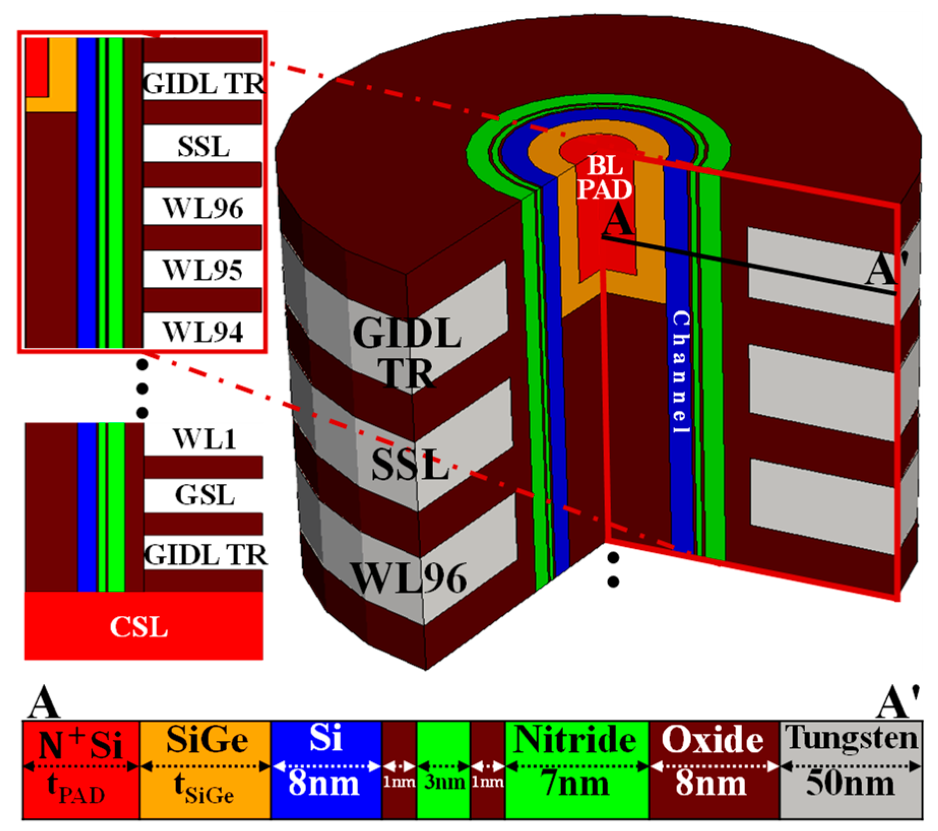
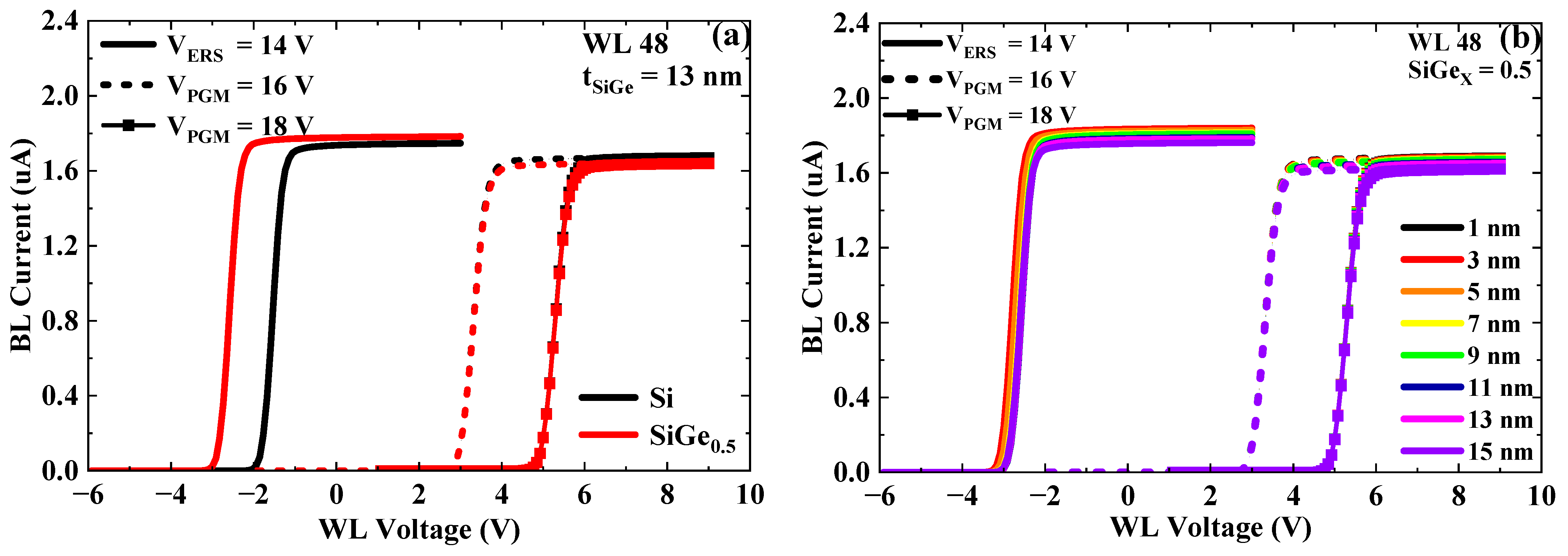
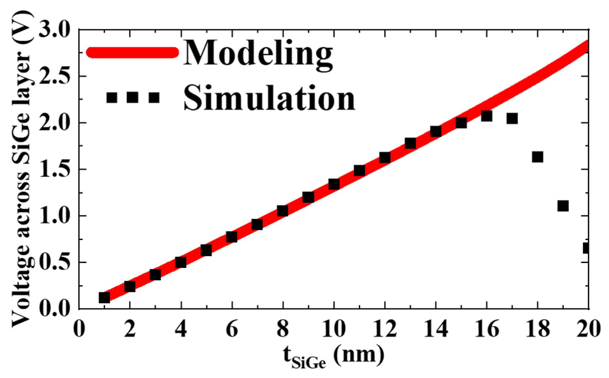
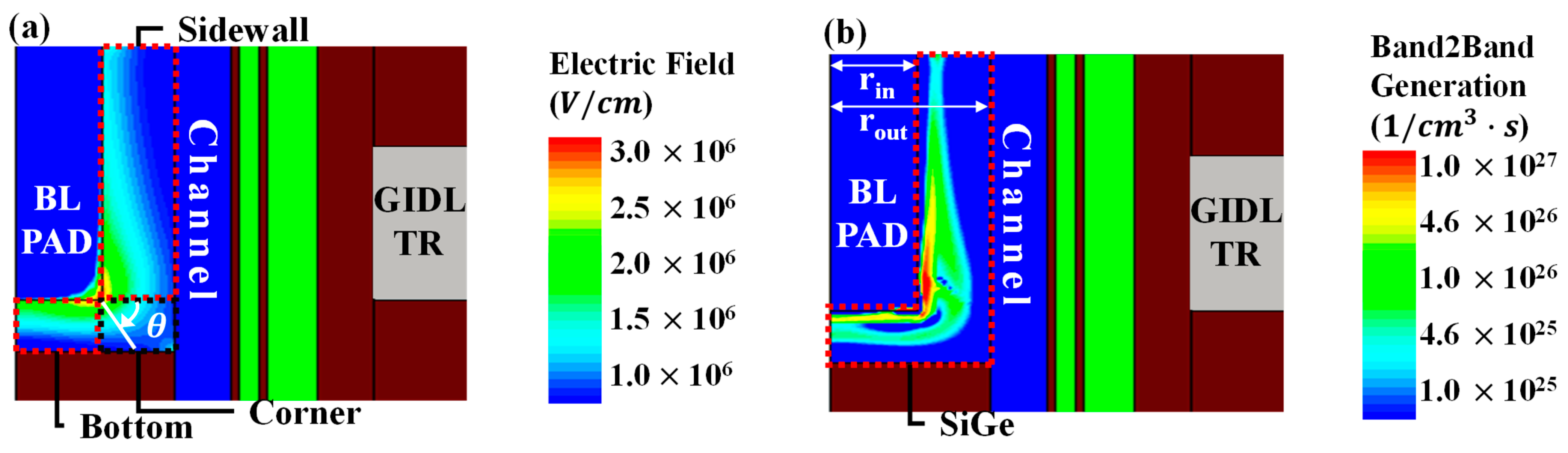
2. SiGe-Surrounded BL PAD Structure and Erase Speed Enhancement

Figure 1 shows the cross-sectional view of a 3D NAND with 96 WLs in the COP structure used for the TCAD simulation. The diagram includes detailed material information and layer thicknesses. In this work, we propose an approach in which an undoped SiGe layer surrounds a n+ doped BL PAD. For the device simulation, the SiGe composition was specified by setting the Ge composition ratio (SiGeX) to the desired value.
The carrier recombination model was based on Shockley–Read–Hall (SRH) processes with doping dependence, while BTBT was modeled using the Hurkx formulation [16]. Carrier transport employed the Philips unified mobility (PhuMob) model calibrated for arsenic doping, supplemented by an electric field normal to the interface (Enormal) high-field saturation correction to capture velocity saturation effects. Meanwhile, in the nitride layer, we introduced donor trap energy level of 2.5 eV below the conduction band and acceptor traps 1.0 eV below the conduction band, each at a density of 1 × 1020 cm−3 with electron and hole capture cross-sections of 1 × 10⁻¹³ cm2.
Next, Table 1 shows the operating voltages for the program, erase, and read operations in 3D NAND Flash. Figure 2 presents the timing diagrams for the erase sequences. As shown in Figure 2, the erase voltage VERS is applied simultaneously to the BL and common source line (CSL), while the GIDL transistor (GIDL TR), string-select line (SSL), and ground-select line (GSL) are held at a fixed 10 V. The erase operation is divided into a 0.1 ms ramp-up phase followed by a 1 ms erase execution phase. The VPGM is applied to the selected WL for 30 µs, while the SSL, GSL, GIDL TR, and unselected WLs are held at 7 V and the BL and CSL are held at 0 V. The erase operation is performed across the entire string, while the program operation is carried out only on the selected WL.
Figure 3 shows the portion of the energy band diagram along the A–A′ cut in Figure 1 for a SiGe thickness of 5 nm. The band diagram was taken immediately after the 0.1 ms ramp-up of the 14 V erase voltage. It highlights how the bandgaps of the pure Si (SiGe0) and SiGe0.5 materials differ. The horizontal axis shows the position along the A–A′ direction, and the vertical axis shows energy level. Because SiGe0.5 has a narrower bandgap than Si (SiGe0), electrons can tunnel more readily from the valence band into the conduction band, yielding a higher BTBT rate. This explains the differences in average channel potential rise and GIDL current observed in Figure 4 and Figure 5 as functions of Ge composition ratio and tSiGe.
Figure 4 shows the average channel potential for various Ge composition ratios. The SiGe bandgap shrinks as x increases [17], directly boosting the BTBT rate in the SiGe layer, which in turn accelerates the average channel potential rise and boosts the GIDL current during the erase operation. Figure 4 confirms that the SiGe-surrounded device sustains higher GIDL current than the Si-only case, with SiGe0.5 achieving 2775% higher GIDL current than SiGe0 at 0.1 ms.
Figure 5 illustrates how tSiGe affects the average channel potential at a fixed Ge ratio of 0.5. When calculating capacitance for a parallel-plate capacitor, the capacitance is inversely proportional to its dielectric thickness. For a cylindrical capacitor, the capacitance is inversely proportional to the natural logarithm of the ratio of its outer radius and inner radius. If we define this value as the effective thickness of a cylindrical capacitor, the effective thickness increases superlinearly with the layer thickness. This means the capacitance of a cylindrical capacitor decreases more rapidly as thickness increases, compared to the parallel-plate structure. Therefore, the voltage-division rule causes the voltage across the SiGe layer in the cylindrical structure to increase superlinearly with the layer thickness. Consequently, the electric field in the SiGe layer increases as the thickness increases, causing higher BTBT rate and accelerating the rise of the average channel potential. However, beyond a tSiGe of 16 nm, the BL PAD area reduction causes a steep rise in its series resistance. Although the BTBT-active region grows, the high resistance of cylindrical BL PAD region hinders the potential increase and hole generation, so the erase operation time increases significantly and limits its use in actual devices.
Figure 6 shows a detailed comparison of the erase threshold voltage shift (ΔVth) as a function of Ge composition ratio for different tSiGe values under (a) a 0.5 ms and (b) a 1 ms erase execution time. When the erase execution time is shorter, the Ge composition ratio has larger impact on the threshold voltage shift. This indicates that increasing Ge composition ratio is essential for reducing the erase execution time. Additionally, for a Ge composition ratio exceeding 0.3, a thinner tSiGe layer results in the highest ΔVth. This is due to the increased series resistance caused by the thicker undoped SiGe layer itself, inducing 0.2~0.3 V of voltage drop in the SiGe region and reducing the maximum voltage reaching the channel. The reduced voltage eventually limits the saturating channel potential level. However, since a higher erase voltage at the BL can easily offset this voltage drop effect, we can fully obtain the erase speed improvement benefit resulting from the increased SiGe thickness.
We confirmed that applying a SiGe layer does not degrade the read performance. As shown in Figure 7, increasing the Ge ratio reduces the read on-current because the electron and hole mobility of SiGe drop by up to 80% and 25%, respectively. In Figure 7, the read on-current gradually decreases as the tSiGe increases, reflecting both the material’s lower mobility and the increased series resistance of a thicker layer. However, on-current decrease relative to the mobility degradation is small because the SiGe layer occupies only a small fraction of the total area, limiting its impact on overall current. Since the maximum on-current reduction remains within 4%, the erase process can still be accelerated by up to 861% with only a minimal effect on read performance. Considering the large resistance and capacitance of WL and BL of 3D NAND array, 4% on-current degradation of the 3D NAND string is ignorable for read latency.
As shown in Figure 4 and Figure 5, the GIDL current reaches its peak at 0.1 ms, which corresponds to the end of the ramp-up phase of the erase operation. Therefore, we designated this timepoint as the reference for modeling in Section 3.

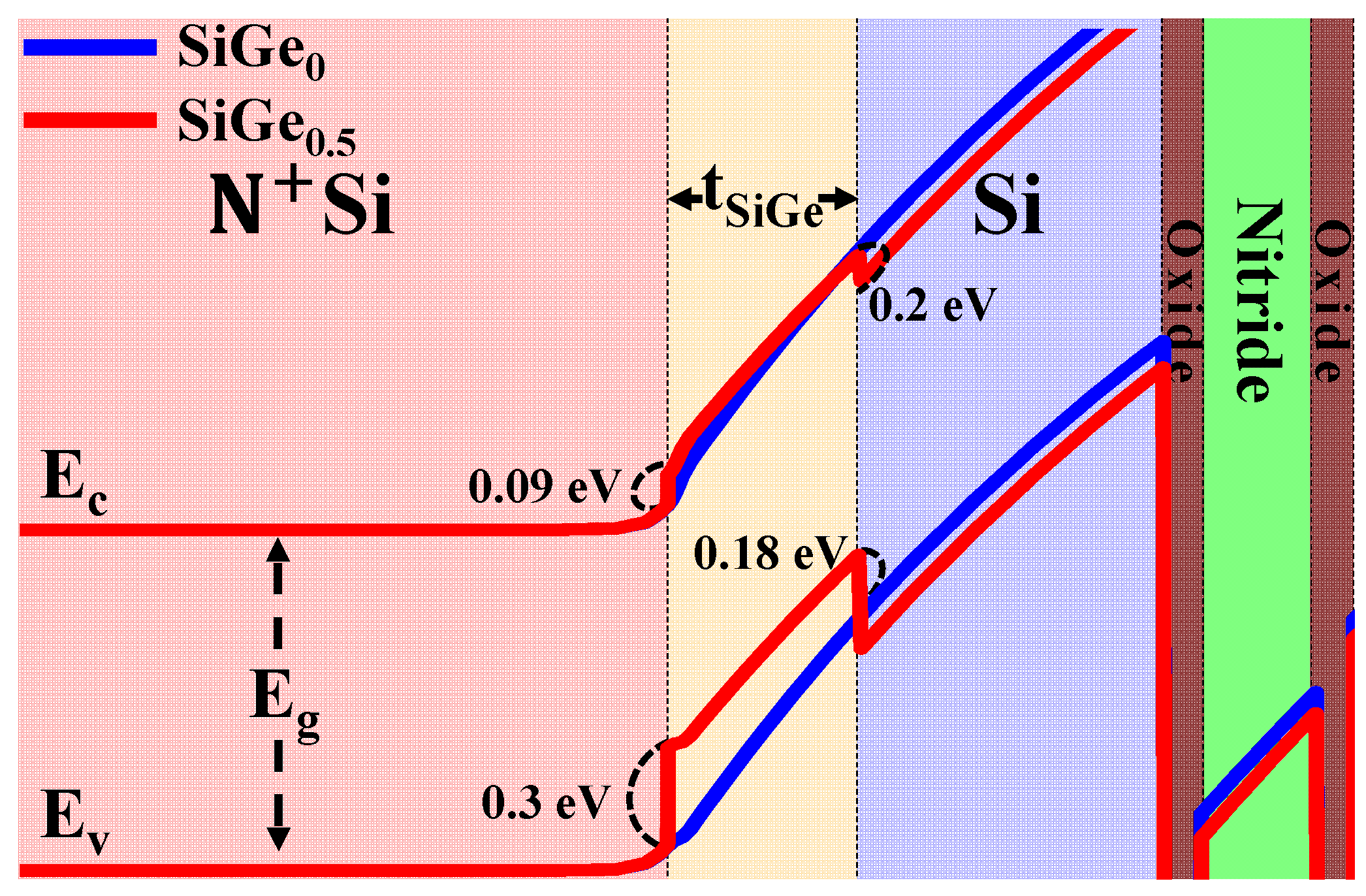
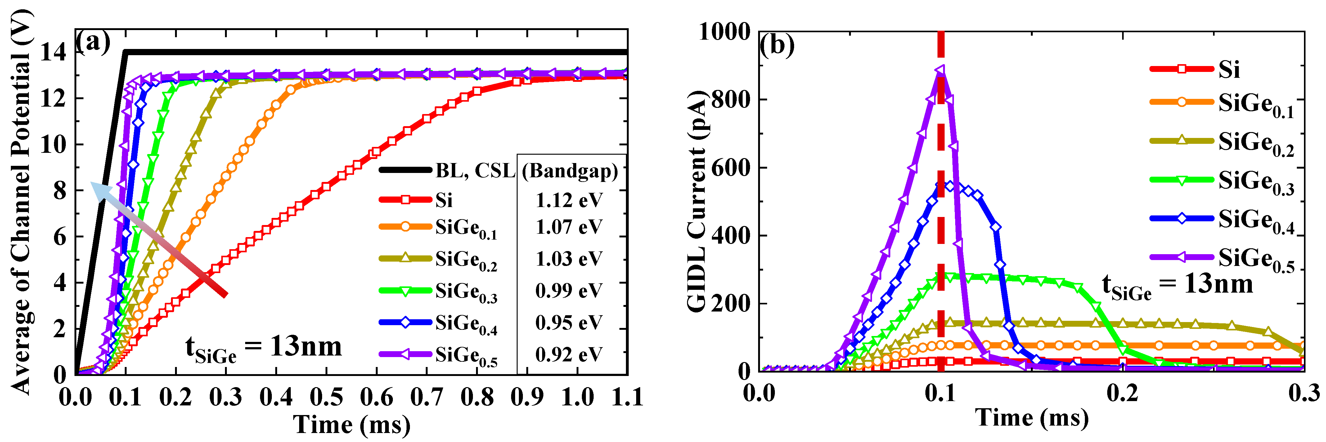
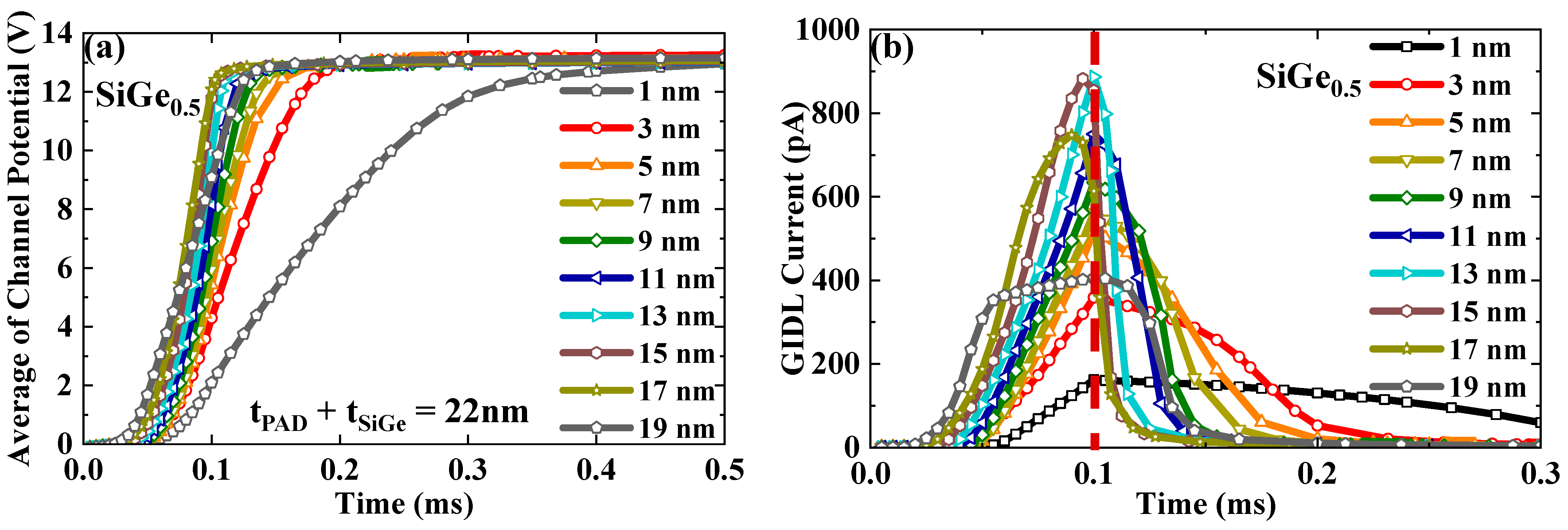
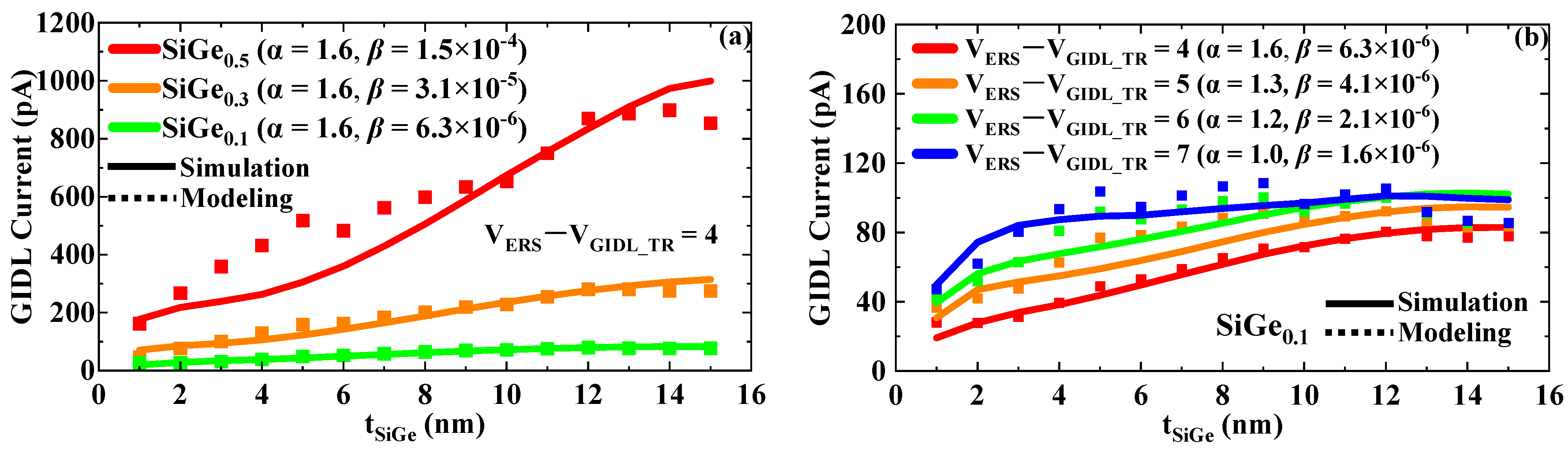
3. Modeling of GIDL Erase with SiGe Surrounded Structures

In this section, we provide a detailed explanation of the methodology and modeling results of the erase operation of the SiGe integrated structure. First, we derived the capacitance of each layer between the BL PAD and the GIDL transistor over the A–A′ region in Figure 1 using the cylindrical capacitance calculation method to calculate the voltage across all layers during the erase operation. Figure 8 compares the voltage across the SiGe layer of cylindrical capacitor modeling results and the TCAD simulation results for different tSiGe values. When tSiGe is below 15 nm, the difference between the modeling results and the TCAD simulation results is at most 5%, demonstrating a high accuracy of the model. However, when tSiGe is thicker than 16 nm, as mentioned in Section 2, the reduction in the BL PAD area causes its resistance to increase, preventing the BL PAD potential from reaching the intended level in time. As a result, a voltage discrepancy arises between the TCAD simulation and the modeling results. Therefore, we excluded the electrical characteristics modeling for the cases of tSiGe over 16 nm in this work.
Figure 9 shows the distribution of the induced electric field and the resulting net generation–recombination rate via BTBT ( R n e t b b ) in the SiGe layer when tSiGe is 13 nm, Ge composition ratio is 0.5, and 14 V applied to BL. Here, rin denotes the radius of the BL PAD, and rout denotes the outer radius including the SiGe layer. The average electric field (Eavg_SiGe) in the sidewall and bottom region of the SiGe layer was modeled as a function of tSiGe as Equation (1). Ctotal is the equivalent series capacitance of bandgap-engineered ONO layer, channel poly-Si layer, and SiGe layer. Since the electric field in the surface region near the BL is significantly larger than elsewhere and R n e t b b in this area dominates the total hole generation, this part was mainly considered in the modeling. The calculated Eavg_SiGe was used to determine the surface electric field (Esur) as defined in Equation (2). The parameter α in Equation (2) is a fitting parameter that adjusts the surface electric field according to the VERS-VGIDL_TR value. Additionally, the electric field in the corner region (Ecor) was also separately modeled, as described in Equation (3).
E a v g _ S i G e = V S i G e t S i G e = ( V E R S V G I D L _ T R ) C t o t a l C S i G e t S i G e
E s u r ( r ) V / c m = ( E a v g _ S i G e r i n + r o u t 2 r d E s u r ( r ) d r ) α
E c o r ( r , θ ) V / c m = E s u r ( r ) cos θ
Based on the individually calculated Esur and Ecor, we calculated the R n e t b b occurring in each region during the erase operation using Equations (4) and (5) from the Hurkx model [16,18]. Equation (5) defines the correction factor D used in the Hurkx model when computing the R n e t b b . Here, n and p are the electron and hole concentrations, respectively, and ni is the intrinsic carrier concentration. The parameter β in Equation (4) is a correction factor varying with the Ge composition ratio and VERS-VGIDL_TR, and Esur or Ecor is assigned to E in Equation (4) depending on the location of R n e t b b . As Ge composition ratio increases, the bandgap narrows and R n e t b b increases.
By integrating R n e t b b for the whole SiGe region at the 0.1 ms point during the erase operation, we modeled the total GIDL current IBTBT_total as Equation (6). The comparison results between the TCAD simulation and modeling for various tSiGe, Ge composition ratio, VERS-VGIDL_TR are shown in Figure 10.
R n e t b b   [ / c m 3 · s e c ] = 3.5 β D E 2 e x p ( 2.25 / E )
D = n p n i 2 ( n + n i ) ( p + n i )
I B T B T _ t o t a l   A = S i G e q R n e t b b

4. Conclusions

This study demonstrates the feasibility of a SiGe-based structure for improving the erase speed of 3D NAND Flash. For this approach, a simple low-pressure chemical vapor deposition (LPCVD) process is used to deposit undoped poly-Si, followed in the same step by the introduction of GeH4 to form SiGe, thereby ensuring full compatibility with standard 3D NAND fabrication flows. Through a simple SiGe deposition that is fully compatible with 3D NAND fabrication process, it can be a solution to achieve faster erase speed in future COP structures of which the number of WLs exponentially increases and the channel capacitance becomes significantly larger. Since GIDL erase is expected to be used in next-generation 3D NAND with hybrid bonding technology [19], our proposal remains effective and applicable.

Author Contributions

Conceptualization, D.K. and W.S.; methodology, D.K. and W.S.; software, D.K.; validation, D.K.; formal analysis, D.K. and W.S.; investigation, D.K.; resources, D.K. and W.S.; data curation, D.K.; writing—original draft preparation, D.K.; writing—review and editing, D.K. and W.S.; visualization, D.K.; supervision, W.S.; project administration, W.S.; funding acquisition, W.S. All authors have read and agreed to the published version of the manuscript.

Funding

This work was supported by the IITP (Institute of Information & Communications Technology Planning & Evaluation)-ITRC (Information Technology Research Center) grant funded by the Korea government (Ministry of Science and ICT) (IITP-2025-RS-2022-00156295).

Institutional Review Board Statement

Not applicable.

Informed Consent Statement

Not applicable.

Data Availability Statement

The data presented in this study are available on request from the corresponding author. The data are not publicly available due to research security.

Acknowledgments

The EDA tool was supported by the IC Design Education Center (IDEC), Korea.

Conflicts of Interest

The authors declare no conflicts of interest.

References

  1. Parat, K. NAND Technology. In Proceedings of the IEEE Hot Chips 25 Symposium (HCS), Stanford, CA, USA, 25–27 August 2013; pp. 1–18. [Google Scholar] [CrossRef]
  2. Tanaka, H.; Kido, M.; Yahashi, K.; Oomura, M.; Katsumata, R.; Kito, M.; Fukuzumi, Y.; Sato, M.; Nagata, Y.; Matsuoka, Y.; et al. Bit Cost Scalable Technology with Punch and Plug Process for Ultra High Density Flash Memory. In Proceedings of the IEEE Symposium on VLSI Technology, Kyoto, Japan, 12–14 June 2007; pp. 14–15. [Google Scholar] [CrossRef]
  3. Jang, J.; Kim, H.; Cho, W.; Cho, H.; Kim, J.; Shim, S.; Goan, Y.; Jeong, J.; Son, B.; Kim, D.; et al. Vertical Cell Array Using TCAT (Terabit Cell Array Transistor) Technology for Ultra High Density NAND Flash Memory. In Proceedings of the Symposium on VLSI Technology, Kyoto, Japan, 15–17 June 2009; pp. 192–193. [Google Scholar]
  4. Seo, Y.; Park, J.K. Improving Z-Interference and Program Disturbance in 3D NAND Flash Memory using Asymmetric Program-pass Voltage. J. Semicond. Technol. Sci. 2024, 24, 565–571. [Google Scholar] [CrossRef]
  5. Oh, Y.-J.; Suh, Y.; Son, S.-W.; Cho, S.; Kang, D.; Cho, I.-H. A Novel Self-aligned Processing for Doubling the Integration Density of 3D NAND Flash Memory. J. Semicond. Technol. Sci. 2025, 25, 199–205. [Google Scholar] [CrossRef]
  6. Kim, J.H.; Yim, Y.; Lim, J.; Kim, H.S.; Cho, E.S.; Yeo, C. Highly Manufacturable 7th Generation 3D NAND Flash Memory with COP Structure and Double Stack Process. In Proceedings of the Symposium on VLSI Technology, Kyoto, Japan, 13–19 June 2021; pp. 1–2. [Google Scholar]
  7. Caillat, C.; Beaman, K.; Bicksler, A.; Camozzi, E.; Ghilardi, T.; Huang, G.; Liu, H.; Liu, Y.; Mao, D.; Mujumdar, S.; et al. 3DNAND GIDL-Assisted Body Biasing for Erase Enabling CMOS under Array (CUA) Architecture. In Proceedings of the IEEE International Memory Workshop (IMW), Monterey, CA, USA, 14–17 May 2017; pp. 1–4. [Google Scholar]
  8. Huh, H.; Cho, W.; Lee, J.; Noh, Y.; Park, Y.; Ok, S.; Kim, J.; Cho, K.; Lee, H.; Kim, G.; et al. 13.2 A 1Tb 4b/Cell 96-Stacked-WL 3D NAND Flash Memory with 30MB/s Program Throughput Using Peripheral Circuit Under Memory Cell Array Technique. In Proceedings of the IEEE International Solid- State Circuits Conference—(ISSCC), San Francisco, CA, USA, 16–20 February 2020; pp. 220–221. [Google Scholar]
  9. Komori, Y.; Kito, M.; Katsumata, R.; Fukuzumi, Y.; Tanaka, H.; Nagata, Y.; Ishiduki, M.; Aochi, H.; Nitayama, A. Disturbless flash memory due to high boost efficiency on BiCS structure and optimal memory film stack for ultra high density storage device. In Proceedings of the IEEE International Electron Devices Meeting (IEDM), San Francisco, CA, USA, 15–17 December 2008; pp. 1–4. [Google Scholar]
  10. Choi, S.; Choi, C.; Jeong, J.K.; Song, Y.-H. Innovative Structure to Improve Erase Speed in 3-D NAND Flash Memory with Cell-on-Peri (COP) Applied. IEEE Trans. Electron Devices 2022, 69, 4883–4888. [Google Scholar] [CrossRef]
  11. Choi, S.; Kang, M.; Song, Y.-H. An Improved Structure Enabling Hole Erase Operation When Using an IGZO Channel in a 3D NAND Flash Structure to Which COP (Cell-On-Peri) Structure Is Applied. Electronics 2023, 12, 2945. [Google Scholar] [CrossRef]
  12. Wang, B.; Gao, B.; Wu, H.; Qian, H. A new 3D NAND flash structure to improve program/erase operation speed. In Proceedings of the International Conference on Electron Devices and Solid-State Circuits (EDSSC), Hsinchu, Taiwan, 18–20 October 2017; pp. 1–2. [Google Scholar]
  13. Lim, S.; Kim, S.; Lee, C.; Choi, H.; Kim, N.; Jung, J.; Yang, H.; Kim, T.-H.; Lim, J.; Ha, D.; et al. Improvement of GIDL-assisted Erase by using Surrounded BL PAD Structure for VNAND. In Proceedings of the IEEE International Memory Workshop (IMW), Monterey, CA, USA, 21–24 May 2023; pp. 1–4. [Google Scholar]
  14. Lee, D.; Liu, T.-J.K. SiGe/Si Heterojunction Drain Transistor for Faster 3D NAND Flash Memory Erase. In Proceedings of the IEEE International Memory Workshop (IMW), Seoul, Republic of Korea, 12–15 May 2024; pp. 1–4. [Google Scholar]
  15. Pratticò, D.; Laganà, F.; Oliva, G.; Fiorillo, A.S.; Pullano, S.A.; Calcagno, S.; De Carlo, D.; La Foresta, F. Integration of LSTM and U-Net models for monitoring electrical absorption with a system of sensors and electronic circuits. IEEE Trans. Instrum. Meas. 2025, 74, 1–11. [Google Scholar] [CrossRef]
  16. Hurkx, G.A.M.; Klaassen, D.B.M.; Knuvers, M.P.G. A new recombination model for device simulation including tunneling. IEEE Trans. Electron Devices 1992, 39, 331–338. [Google Scholar] [CrossRef]
  17. Levinshtein, M.E.; Rumyantsev, S.L.; Shur, M.S. Properties of Advanced Semiconductor Materials GaN, AlN, InN, BN, SiC, SiGe; John Wiley & Sons, Inc.: New York, NY, USA, 2001; pp. 149–185. [Google Scholar]
  18. Sentaurus Device User Guide, Version N-2023.09; Synopsys: Mountain View, CA, USA, 2023.
  19. Lee, S.; Lim, J.; Kim, J.H.; Cho, S.; Lee, Y.K.; Choi, B. High-Density 3-D NAND Cell Array Design with Hybrid Bonding. IEEE Trans. Electron Devices 2023, 70, 5638–5644. [Google Scholar] [CrossRef]
Figure 1. Cross-section of the top part of the simulated 3D NAND string and the details of material and thickness of each layer.
Applsci 15 07405 g001
Figure 2. Timing diagram of erase operations.
Applsci 15 07405 g002
Figure 3. Band diagram of Si (SiGe0) and SiGe0.5 immediately after the ramp-up phase at VERS = 14 V.
Applsci 15 07405 g003
Figure 4. (a) The average channel potential; (b) GIDL current over time for various Ge composition ratios.
Applsci 15 07405 g004
Figure 5. Simulation result with various tSiGe at VERS = 14 V: (a) The average channel potential; (b) GIDL current over time.
Applsci 15 07405 g005
Figure 6. Simulation results with various tSiGe at VERS = 14 V: (a) Erase execution time of 0.5 ms; (b) 1 ms over SiGeX.
Applsci 15 07405 g006
Figure 7. BL Current for (a) different Ge composition ratios; (b) SiGe thickness over WL voltage.
Applsci 15 07405 g007
Figure 8. TCAD simulation and modeling results for the voltage across SiGe layer over tSiGe at VERS = 14 V.
Applsci 15 07405 g008
Figure 9. (a) Distribution of electric field; (b) BTBT generation in the BL PAD and SiGe region at VERS = 14 V.
Applsci 15 07405 g009
Figure 10. (a) GIDL current modeling results according to SiGeX; (b) GIDL current modeling results according to VERS-VGIDL_TR.
Applsci 15 07405 g010
Table 1. Bias Conditions for Program, Erase, and Read Operations in 3D NAND Flash.
ContactEraseProgramRead
BLVERS0 V0.2 V
CSLVERS0 V0 V
SSL10 V7 V7 V
GSL10 V7 V7 V
GIDL transistor10 V7 V7 V
Selected WL0 VVPGMVRead
Unselected WLs0 V7 V5 V
Disclaimer/Publisher’s Note: The statements, opinions and data contained in all publications are solely those of the individual author(s) and contributor(s) and not of MDPI and/or the editor(s). MDPI and/or the editor(s) disclaim responsibility for any injury to people or property resulting from any ideas, methods, instructions or products referred to in the content.

